Final Project - ECE 421L
Project Goal
Design, layout, and simulate a digital receiver circuit that accepts a
high-speed digital input signal D and Di (a differential pair connected to your circuit from, for example, a twisted pair of wires such as in an
Ethernet cable). D and Di are complements so, for example, if D is 5V then Di is 0V and output = 1. Another example, when D is 1V and Di is 2V
then output = 0. At high-speeds and long distances the voltages received aren't full digital logic levels (i.e., 5V and 0V), hence the need to design,
and use, a high-speed digital recevier circuit. Ideally, when D > Di the receiver outputs a 1. When D < Di the receiver outputs a 0. Base your
design on the topology seen in Fig. 18.23. Try to design for high-speed and low-power. Characterize your design (in sims) and the trade-offs.
For example, show that you get higher-speed if you use more energy (burn more power). See if you can get, in this 500 nm process, 250 Mbits/s
(a bit width of 4 ns) with an input voltage difference of, for example, 250 mV (with D and Di swinging back and forth between 2.75V and 3V,
for one of many examples, your circuit outputs the correspondingly correct values). Note that while Fig. 18.23 shows one inverter on the output
you may find, for example, that two inverters work better (at the cost of power). Use a table to summarize your design's performance.
Part 1: Operation
Building the Modules:
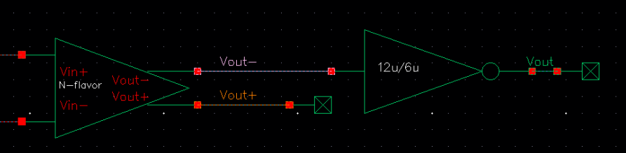
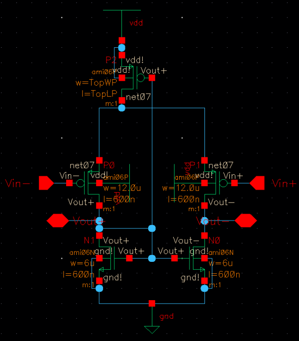
The heart of the digital receiver are input buffers. To start, a self-biasing diff-amp using NMOS inputs is created.
The buffer circuit is then simulated using a symbol.
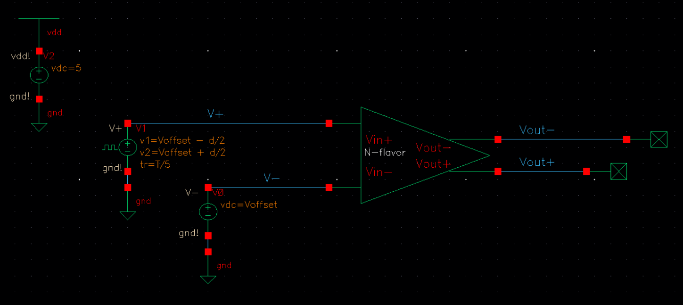
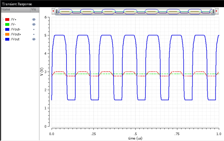
The V- input is held at a constant 2.875V and the V+ oscillates between 2.75V and 3V. The resulting waveform
looks like this (and is taken from the Vout- terminal making it inverted).
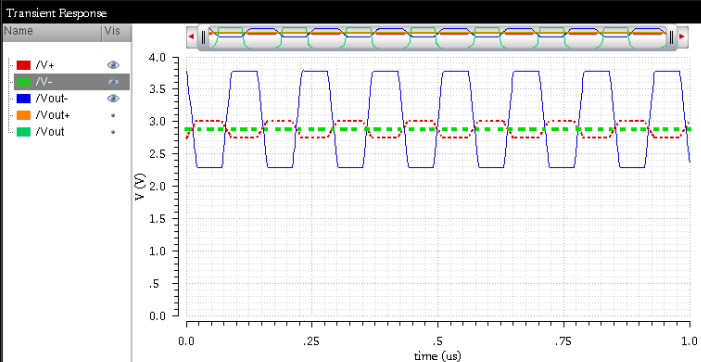
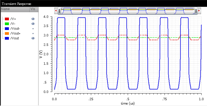
This waveform functions correctly but the output does not reach full logic levels. To solve this, a buffer stage
is added to the output of the diff-amp using an inverter; the inverter also inverts the output so that it matches the
input logically.
Now the output waveform reaches near-full logic levels.
Some issues remain. The output does not reach a full 5V logic level, and transitions for low voltage outputs are not as clean.
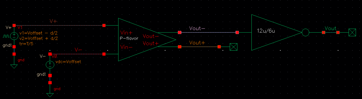
To fix this, an input buffer using PMOS gates as inputs is made.
Simulation shows superior operations to the NMOS based schematic at low voltages, but suffers from simuliar problems when transitioning
at high voltages.
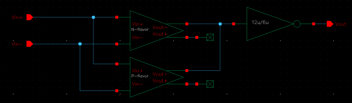
A really useful input-buffer combines both types of input buffers to create a more decisive waveform.
In the simulation below, solid waveforms are produced by combining the NMOS input and PMOS input
self-biased diff-amps.
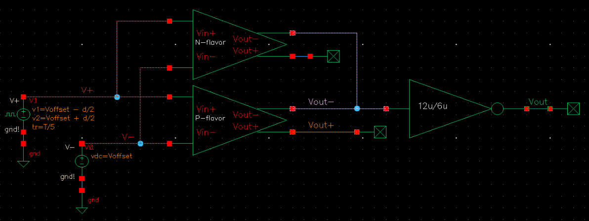
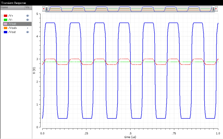
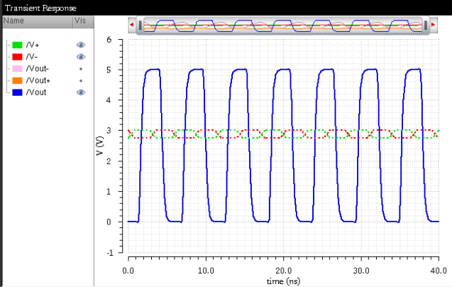
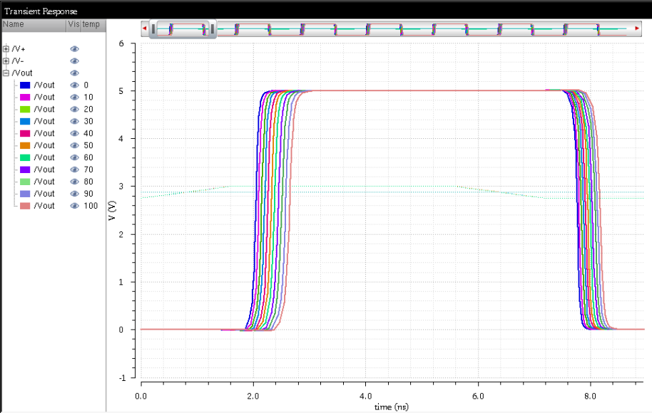
With the current changes, combining the NMOS and PMOS diff-amps and using a buffer on the output, this is the input buffer so far.
The current design works, however the waveform is choppy for high frequency. Lowering the input waveform period to 8ns yields the following
results. Attempting to drive a load would result in a worse waveform.
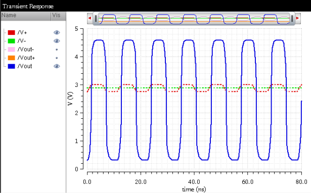
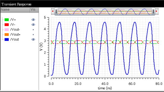
When trying to drive a 1pF load, the following occurs on the output:
This can be resolved by buffering the output using more inverters at the expense of power dissipation from the extra inverters.
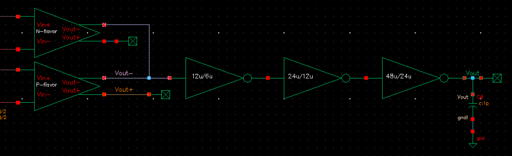
The result is a more clean output waveform that reach full logic levels and can drive a 1pF load for other logic gates
while supporting a bit width of 4ns.
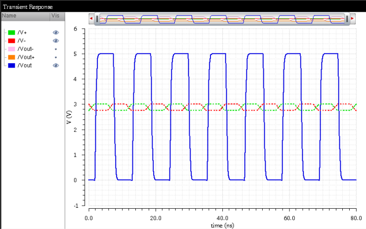
The circuit can also operate with a bit width of 2ns with reduced performance.
Limitations:
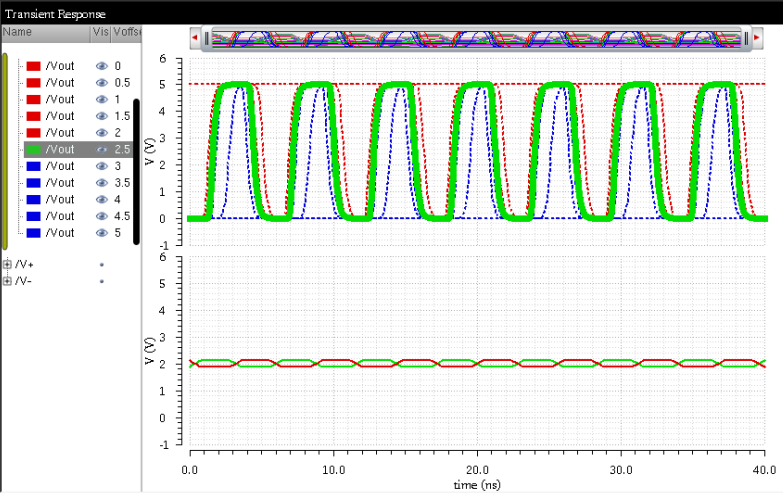
There are some limitations to the configuration. The first being that the input differential signal cannot operate
at any range. The optimal range for the differential signal is to bounce about 2.5V as shown in the simulation below.
At low (relative to Vdd/2) DC operation, the logical high dominates the outputwaveform, taking longer to decrease. While at high
voltage (relative to Vdd/2) the logical low dominates. This may be due to mis-biasing of the transistors.
(Voffset is the voltage that the differential signal swings around, assuming a 250mV difference).
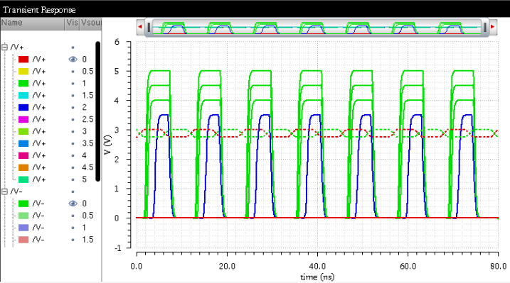
VDD is also mostly stable at 5V. When the voltage drops, the logical high bit width becomes degenerated. If VDD is too low,
especially lower than the input DC voltage, the output completely collapses as shown in the following graph (where Vsource is VDD voltage).
Power Consideration:
To examine the power dissipation, the power dissipated by the two diff-amps is examined, then the
power dissipated by the buffers. To do such, the current through the bottom NMOS and top PMOS
is examined (the current through the circuit) and multiplied by the VDD value.
(P = I * V)
This is done at multiple L values first. Here is the calculator data from CADENCE along with the formula used.
This is done for a bit-width of 4ns.
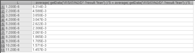
L P
| 1.2µm | 6.314mW |
| 2.2µm | 4.588mW |
| 3.2µm | 3.650mW |
| 4.2µm | 3.047mW |
| 5.2µm | 2.622mW |
| 6.2µm | 2.306mW |
| 7.2µm | 2.061mW |
| 8.2µm | 1.865mW |
| 9.2µm | 1.705mW |
| 10.2µm | 1.571mW |
| 11.2µm | 1.457mW |
| 5ns | 2.341mW |
| 10ns | 2.325mW |
| 15ns | 2.321mW |
| 20ns | 2.319mW |
| 25ns | 2.318mW |
| 30ns | 2.317mW |
| 35ns | 2.317mW |
| 40ns | 2.316mW |
| 45ns | 2.316mW |
| 50ns | 2.316mW |
| 5ns | 4.012mW |
| 560ns | 2.783mW |
| 1.115µs | 2.782mW |
| 1.670µs | 2.782mW |
| 2.225µs | 2.782mW |
| 2.780µs | 2.782mW |
| 3.335µs | 2.782mW |
| 3.890µs | 2.782mW |
| 4.445µs | 2.782mW |
| 5µs | 2.782mW |
| 5ns | 2.206mW |
| 560ns | 257.3µW |
| 1.115µs | 242.7µW |
| 1.670µs | 238.3µW |
| 2.225µs | 236.4µW |
| 2.780µs | 235.5µW |
| 3.335µs | 234.9µW |
| 3.890µs | 234.5µW |
| 4.445µs | 234.3µW |
| 5µs | 234.1µW |
| 5ns | 1.4mW |
| 560ns | 122.8µW |
| 1.115µs | 82.77µW |
| 1.670µs | 66.32µW |
| 2.225µs | 61µW |
| 2.780µs | 56.61µW |
| 3.335µs | 53.6µW |
| 3.890µs | 51.48µW |
| 4.445µs | 49.86µW |
| 5µs | 48.6µW |
| 5ns | 9.908mW |
| 560ns | 4.314mW |
| 1.115µs | 4.285mW |
| 1.670µs | 4.275mW |
| 2.225µs | 4.271mW |
| 2.780µs | 4.268mW |
| 3.335µs | 4.266mW |
| 3.690µs | 4.265mW |
| 4.445µs | 4.264mW |
| 5µs | 4.263mW |
The following simulation shows the result of operating the circuit at various different
temperatures. There is little difference, however, as temperature increases, the delay
of the output appears to increase.
Results at 8ns clock.
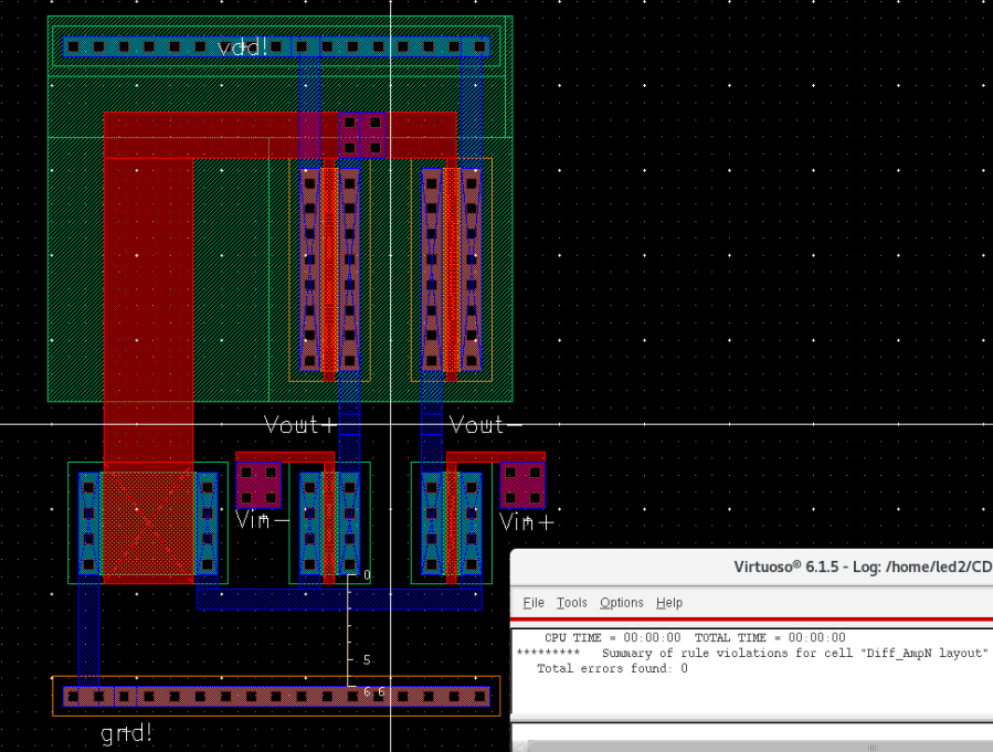
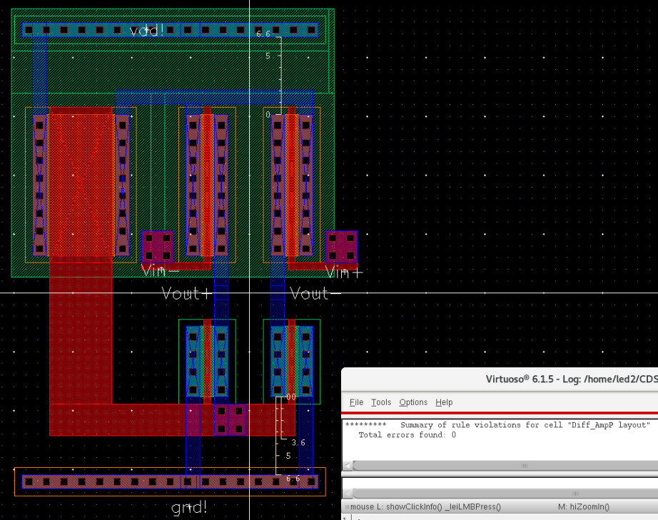
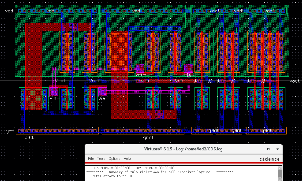
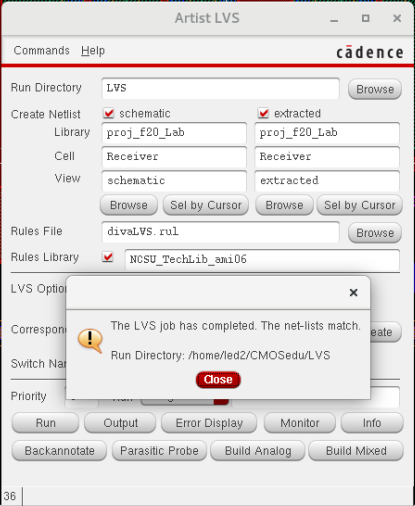
Part 2: Layout
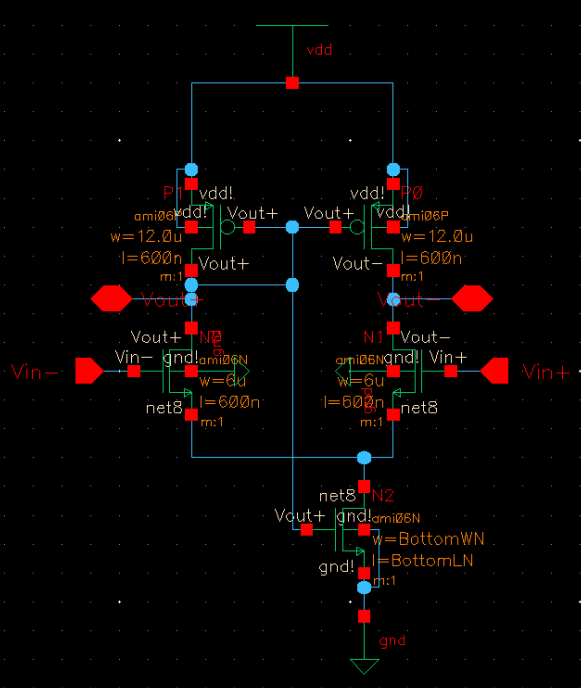
In the second part of the project, a layout is made. Three modules are laid out—the N-flavor, P-flavor diff-amps,
and the final receiver module.
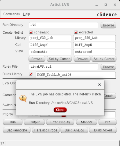
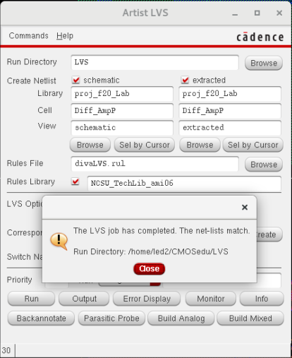
Shown here is the layout of the N-flavor diff-amp. The diff-amp passes the DRC and LVS check.