Lab 7 - ECE 421L
Authored
by Do Le (led2@unlv.nevada.edu)
21st of October, 2020
Lab Description
The purpose of this lab is to work with buses and arrays of components.
During the lab schematics were created for the inverter, NAND gate, NOR gate, AND gate,
and OR gate. 8-bit word versions of the gates were created by using buses.
Mux/Demux were also created along with their 8-bit word versions.
Using full adders, an 8-bit adder was designed and laid out.
Prelab
Ring-Oscillator
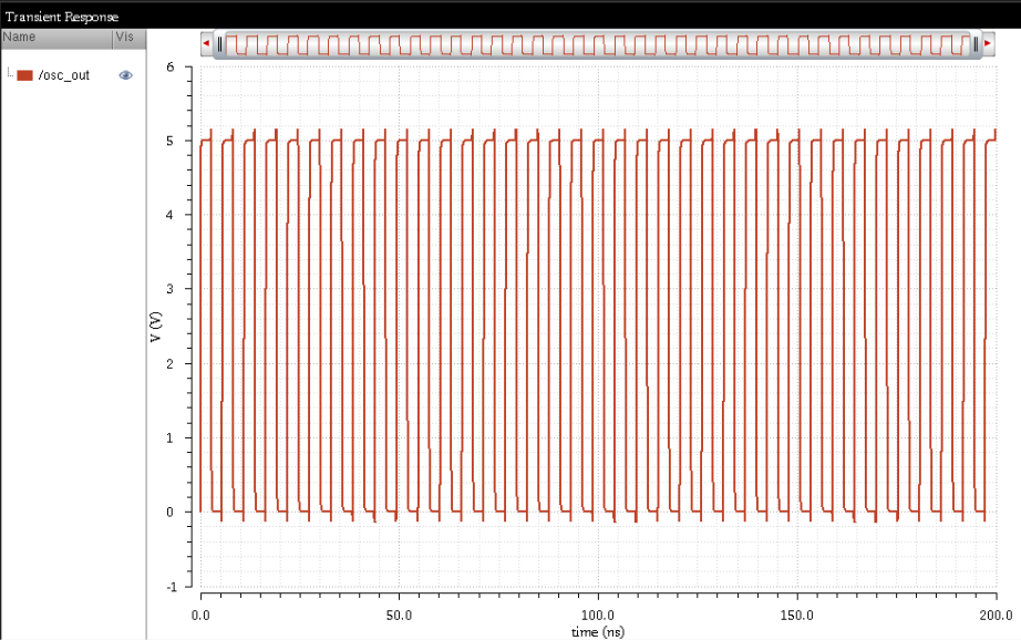
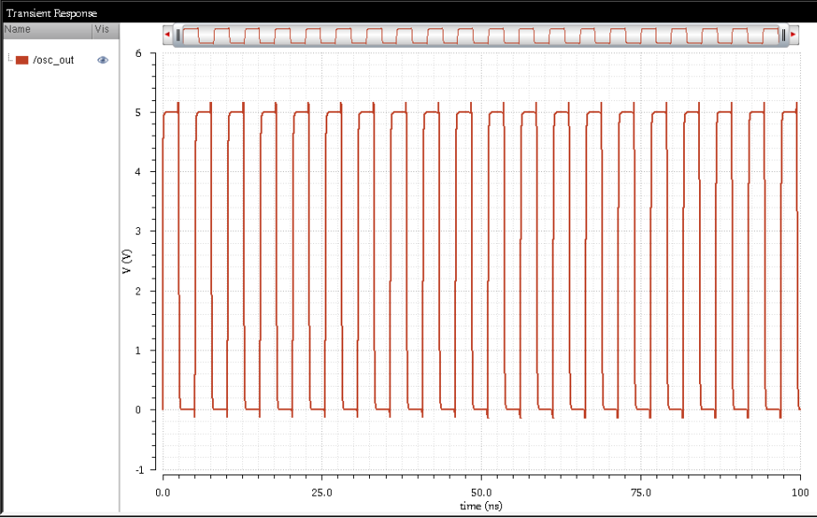
During the pre-lab, a ring-oscillator—a circuit that generates constant pulses was made.
The ring oscillator was made using 31 inverters connected in series with a feedback loop.
Here is the resulting schematic.

Simulation of the circuit yields the following waveform.
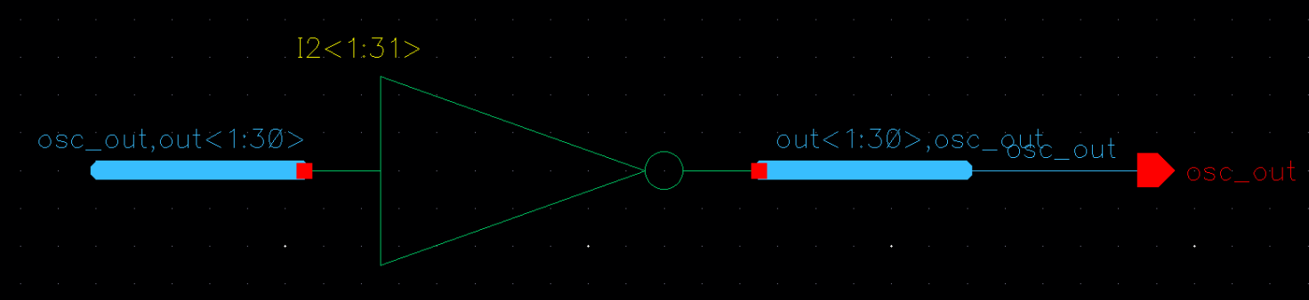
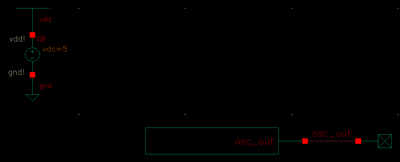
The schematic view for the oscillator is not compact enough, but can be
replicated exactly using the following schematic.
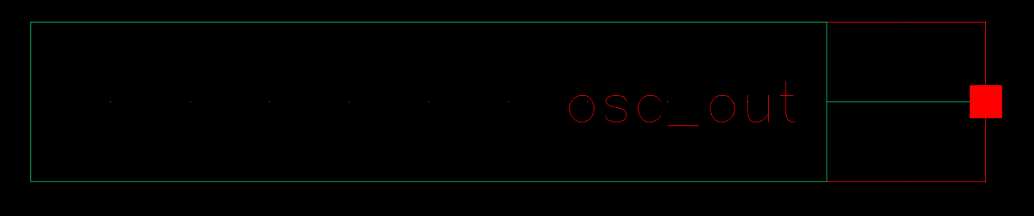
A symbol was made for the ring oscillator.
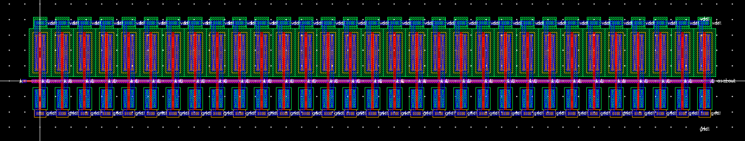
The oscillator can be laid out by using inverter layouts created in
previous labs. To verify that the circuit matches the intended
schematic, an LVS was performed.
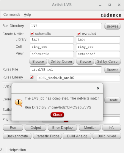
A simulation of the resulting cell shows that the two schematic views are equivalent.
Lab
4x Inverter:
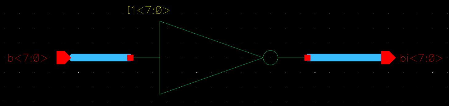
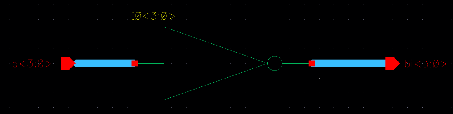
During the first part of the lab, a 4 bit word bus inverter is designed. This is simply created by connecting
four inverters together, however, this can be done easily by using
buses and arrays as shown in the schematic below.
To show that this functions identically to placing down four inverter,
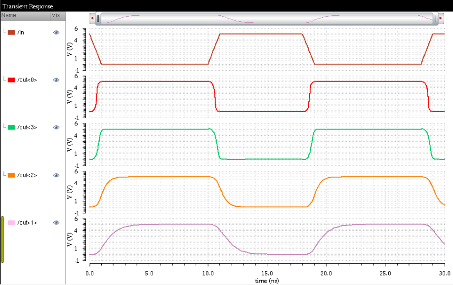
a transient simulation is produced using the resulting symbol.
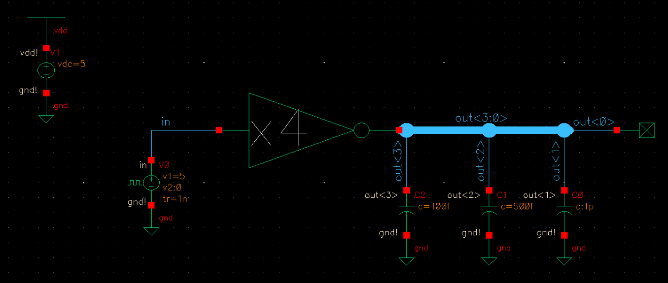
Here are the results:
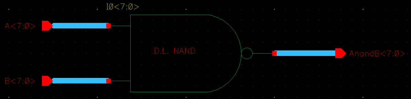
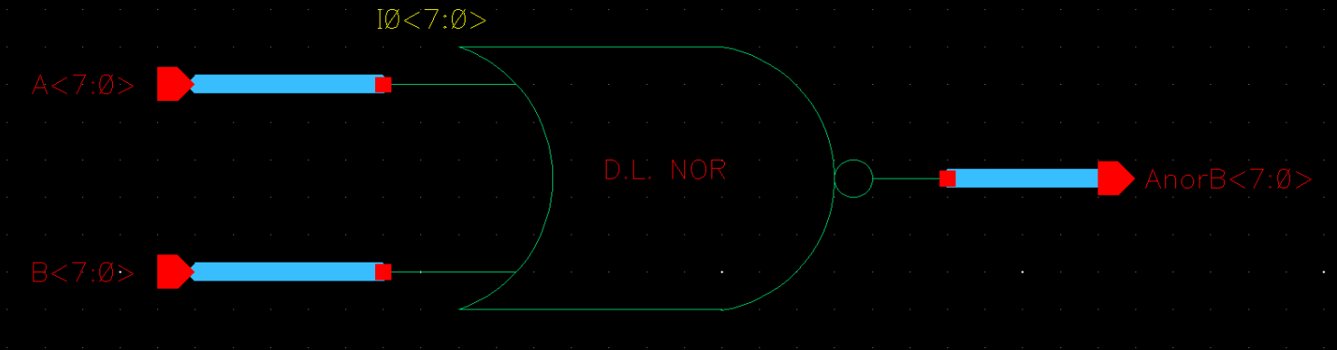
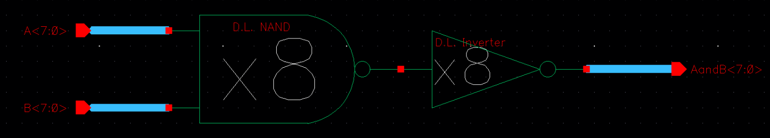
Bus NAND, NOR, AND, NOT, OR:
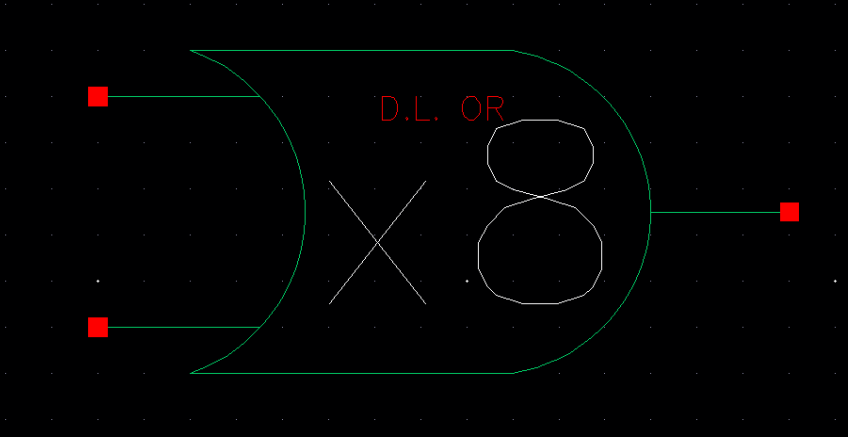
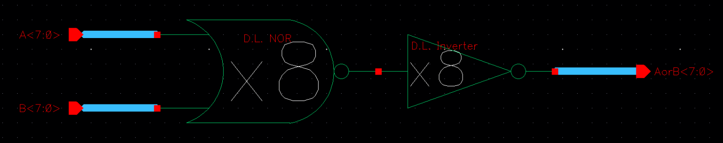
Using these same concepts, we can create 8-bit wide bus gates for the NAND, NOR, AND, NOT, and OR gate.
(Of course, these shortcuts do not apply to layout view).
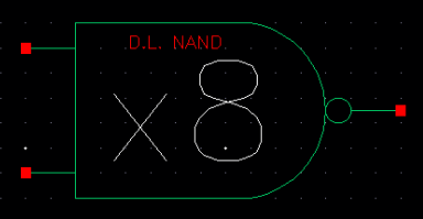
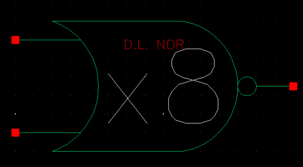
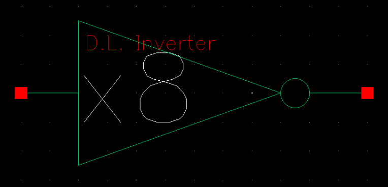
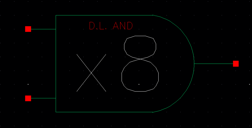
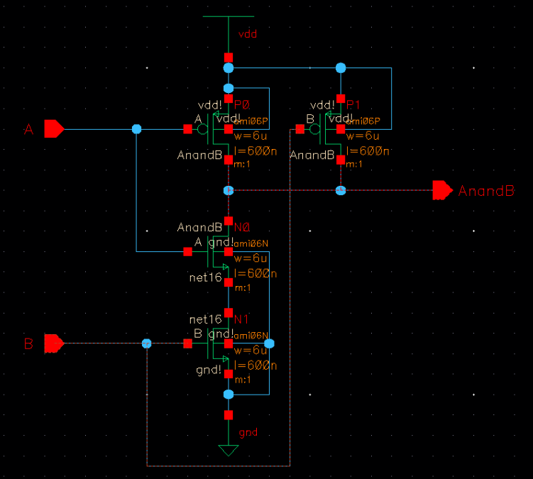
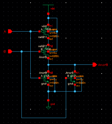
The standard transistor level design of the one-bit input NAND, NOR, and NOT gates are shown.
The table below show the schematic design of each gate and their corresponding symbol.
Nand Transistor Level
Nor Transistor Level
Gates Symbols
Schematic
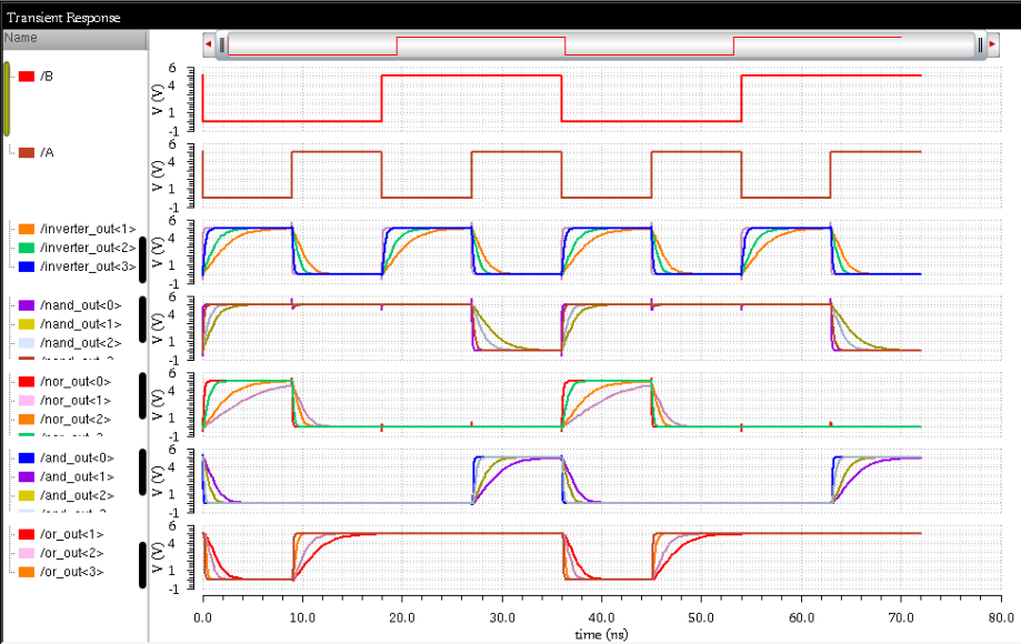
We can perform a simulation of the gates to verify their operation using the following schematic.
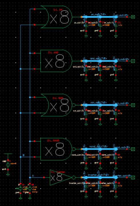
A transient simulation of the above yields predictable results (notice
the various delays due to the load capacitance).
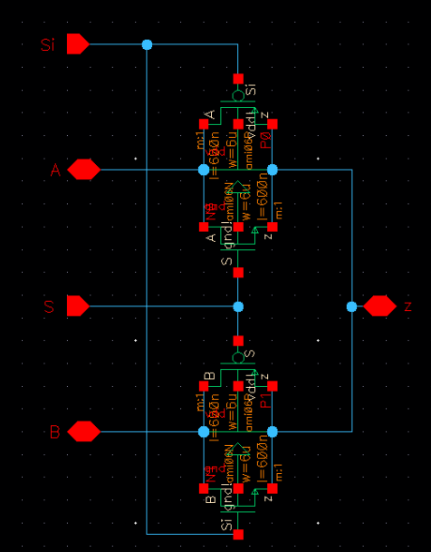
MUX/DEMUX:
MUX and DEMUX gates are gates that allow the signal path to be
selected. In the MUX configuration, the select lines
determine which input signal is taken to the output. In the DEMUX
configuration, the select lines choose which outputs
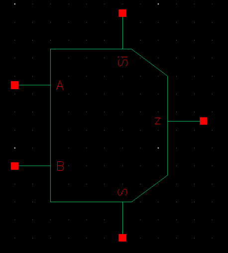
the input connects to. Here is a schematic of a 2 to 1 MUX/DEMUX, along with it's symbol.
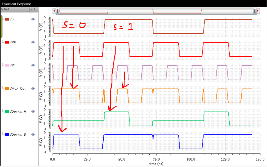
Using this schematic view, the operation of the circuit can be verified.
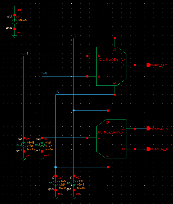
Here are the results of the transient simulation.
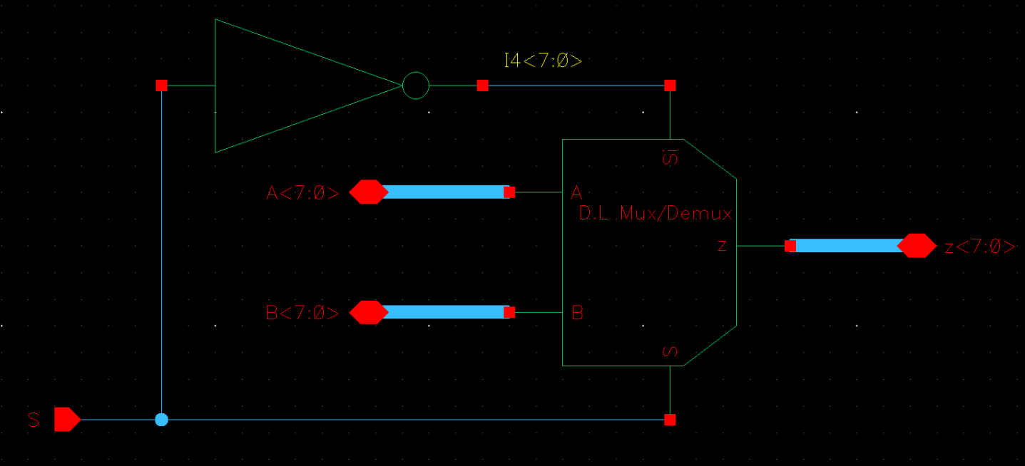
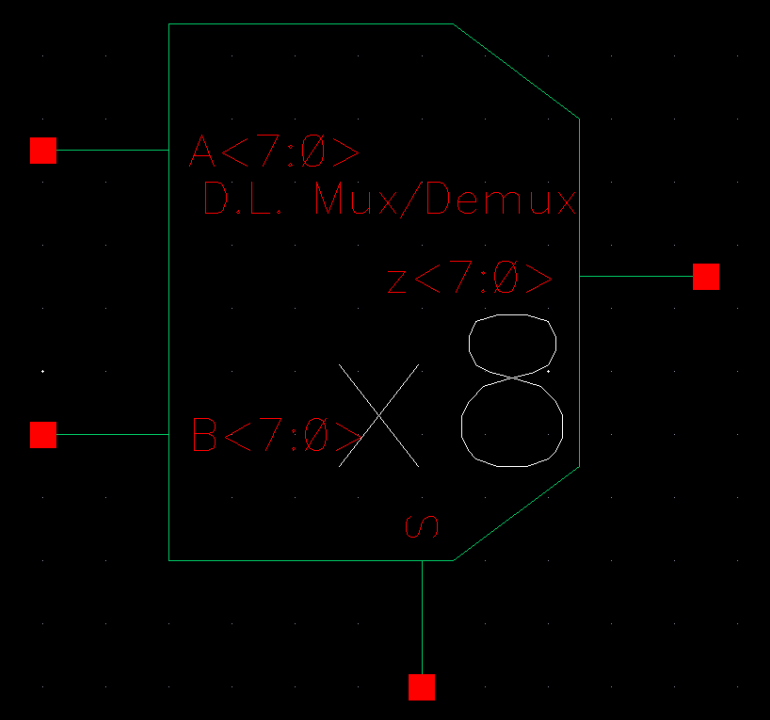
Now we can create 8-bit wide word MUX/DEMUX using the concepts
introduced earlier. To keep signals compact an inverter is used
for Si within the cell. Here is the schematic followed by the new symbol.
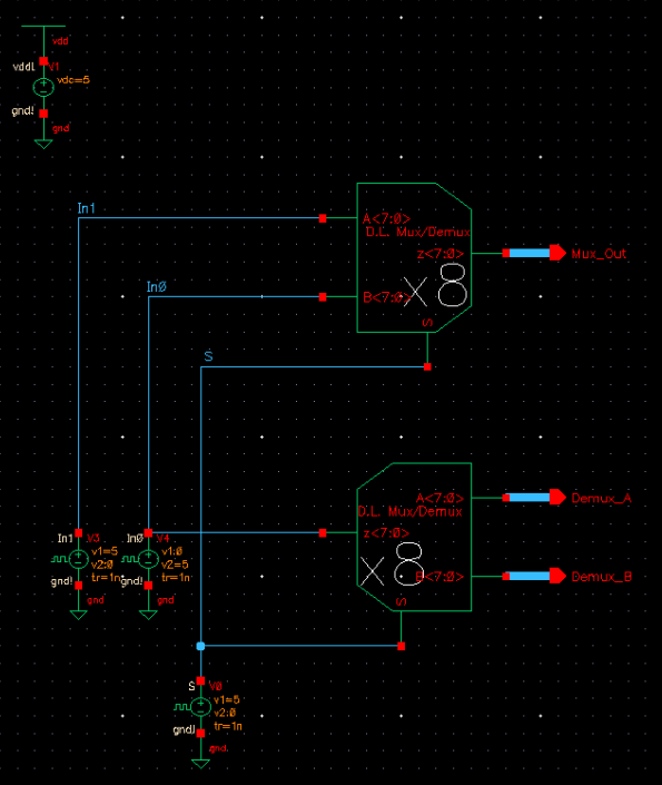
A final verification of the 8-bit word MUX/DEMUX is performed by modifying the original schematic
used for simulation.
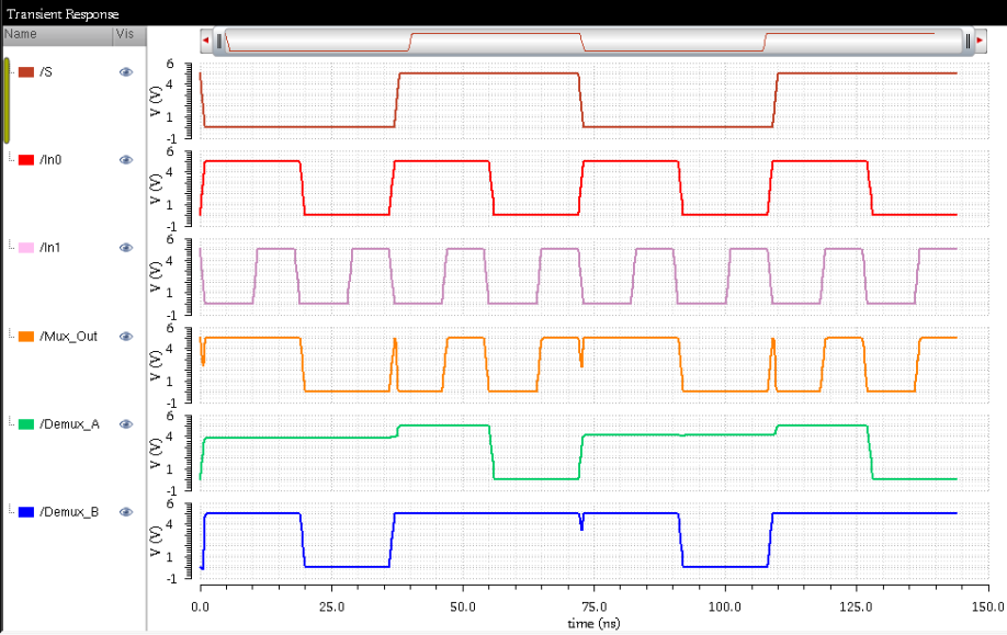
Here are the results.
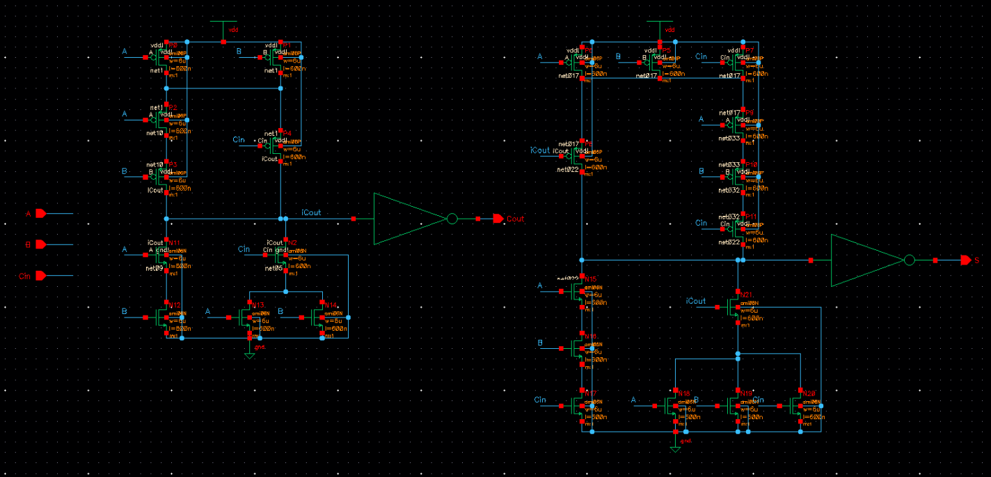
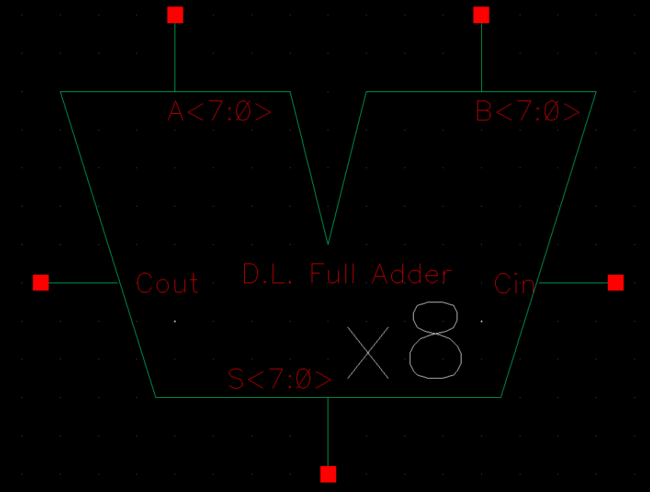
Full Adder:
The final design is of an 8-bit full adder. To start, we design a single full adder that adds
inputs A, B, and Cin and generates a sum result S, and carrout result Cout. This time the whole
full adder is implemented in the transistor level and looks like this.
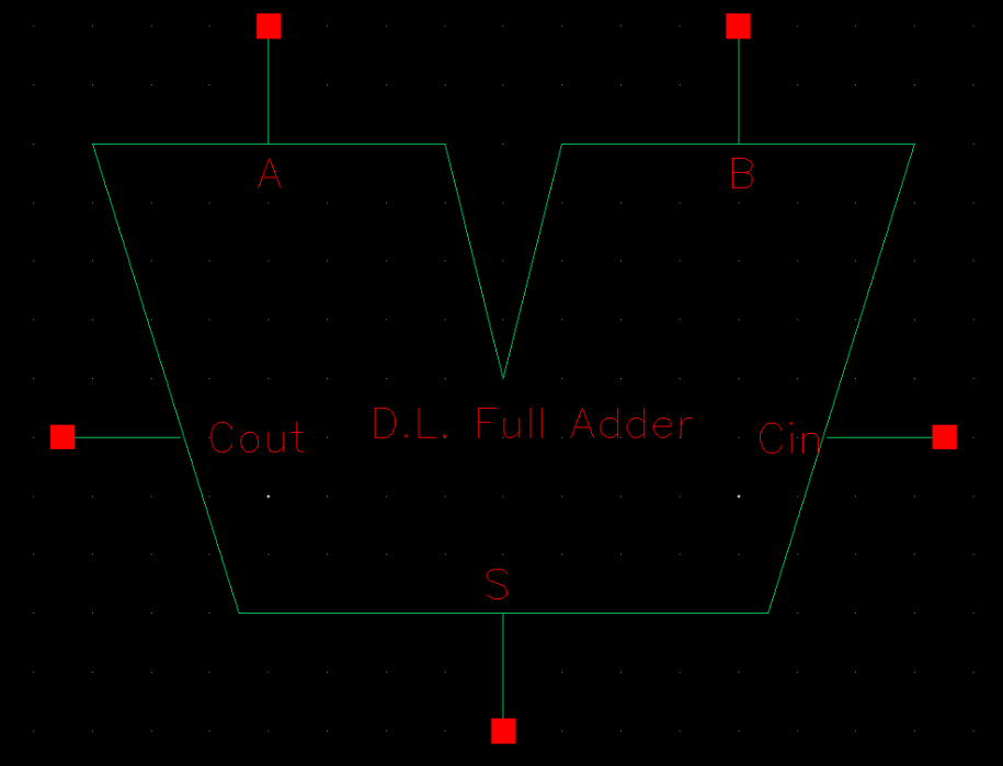
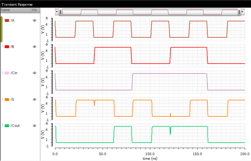
A symbol is created, and simulations are ran using the symbol to verify the operations of the full adder.
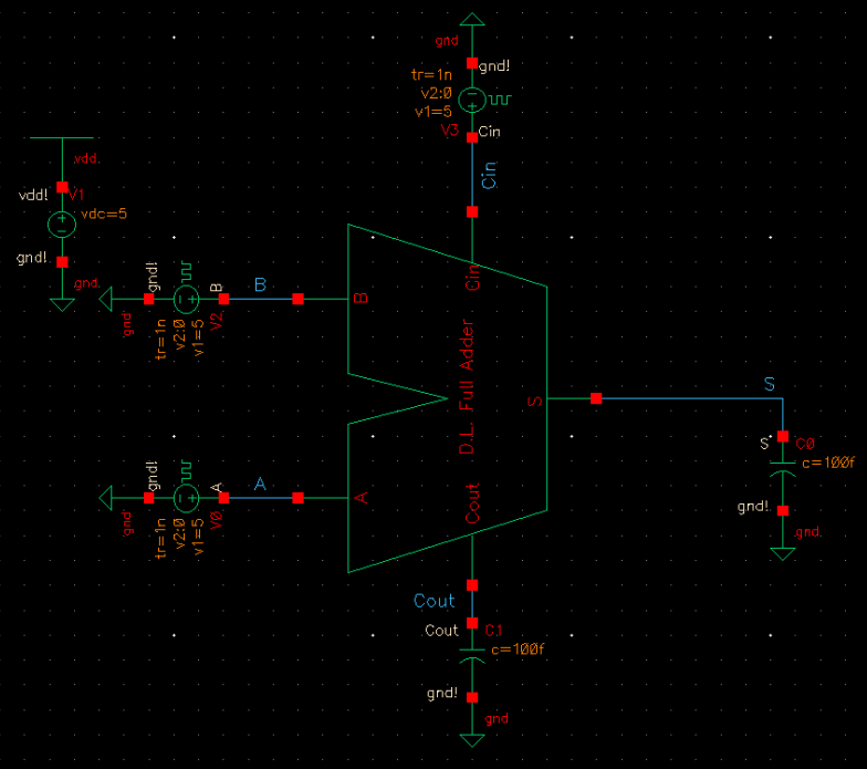
Here are the results of the simulation.
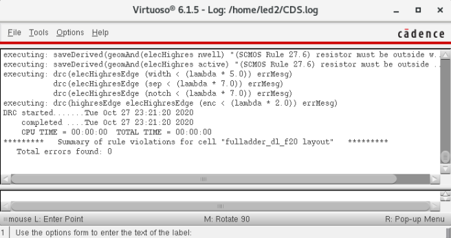
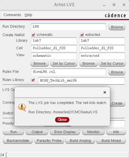
Lastly for the 1-bit full adder, a layout is created. To verify the
specifications are met, an LVS and DRC is done.
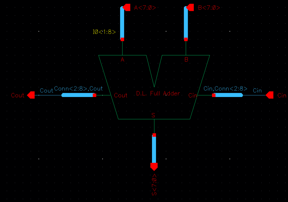
Lastly, an 8-bit adder can be designed using the full adder. Using the bus and array concept, the
schematic view can be created easily, along with a corresponding symbol view.
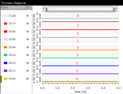
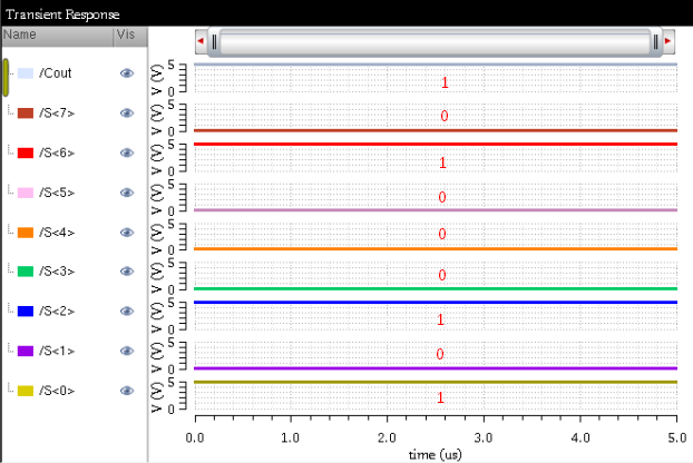
A final verification of the design is done by adding two sets of binary numbers using this schematic.
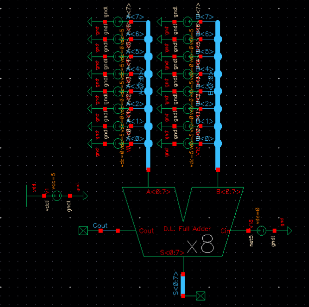
10010110 + 01001010 = 0 11100000
10110010 + 10010011 = 1 01000101
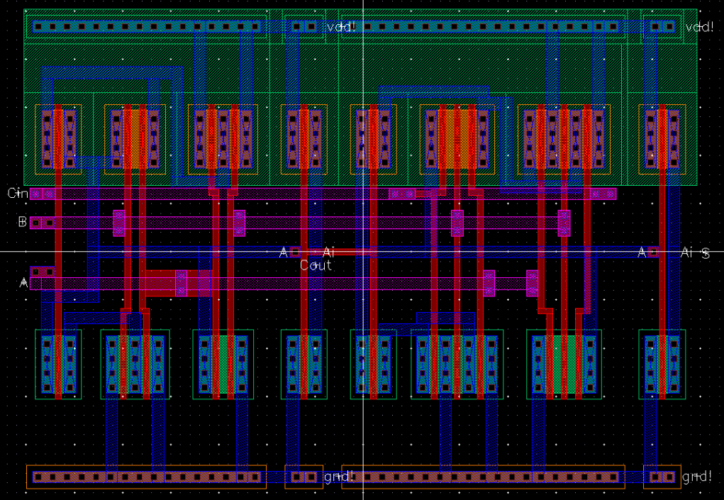
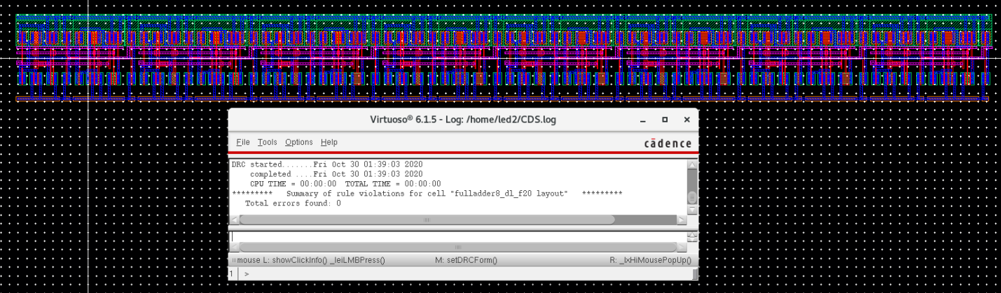
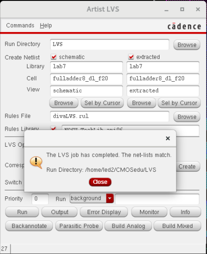
Finally, a layout of the 8-bit adder is made by connecting 8 full
adders' carry out and carry in. Here is the layout with a DRC followed
by LVS.
With the building blocks of an ALU complete, that concludes lab 7.
The cells used in this lab can be found here at lab7_dvl.zip.
Return to led2 lab directory