Lab 6 - ECE 421L
Lab Description
The purpose of this week's lab is to design a full adder starting from the transistor level.
A full adder is a digital logic circuit that can add two bits with an additional carry in bit.
The circuit produces the sum of two bits along with a carry out bit.
The full adder takes three inputs (A, B, Cin) and outputs three bits (S, Cout).
CMOS NAND and XOR gates are used for the logical implementation of the adder.
An inverter was also necessary to implement the XOR gate.
Prelab
Nand Gate:
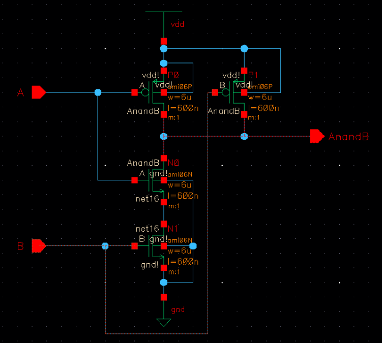
The pre-lab was the design of the CMOS NAND gate. The NAND gate is made with 6µm/600nm
NMOS and PMOS devices. Here is the schematic of the NAND gate.
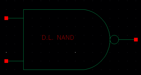
A corresponding symbol is made so that the NAND gate can be used on schematic
view designs. The standard NAND symbol is replicated. (Creator initial is placed inside the symbol).
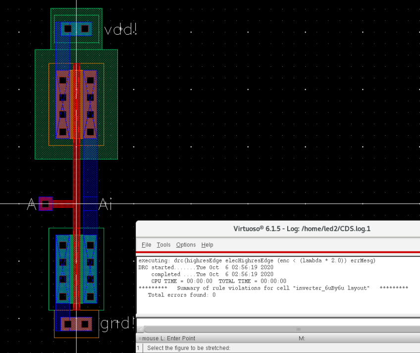
Next, a layoutview of the NAND gate is made. This is done with 6µm/600nm NMOS and PMOS.
A DRC is done to make sure that the design rules are met.
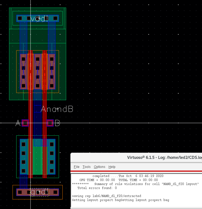
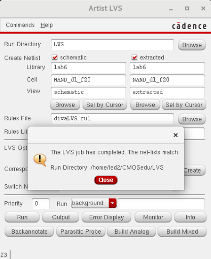
To verify that the layout matches the schematic, an LVS is done.
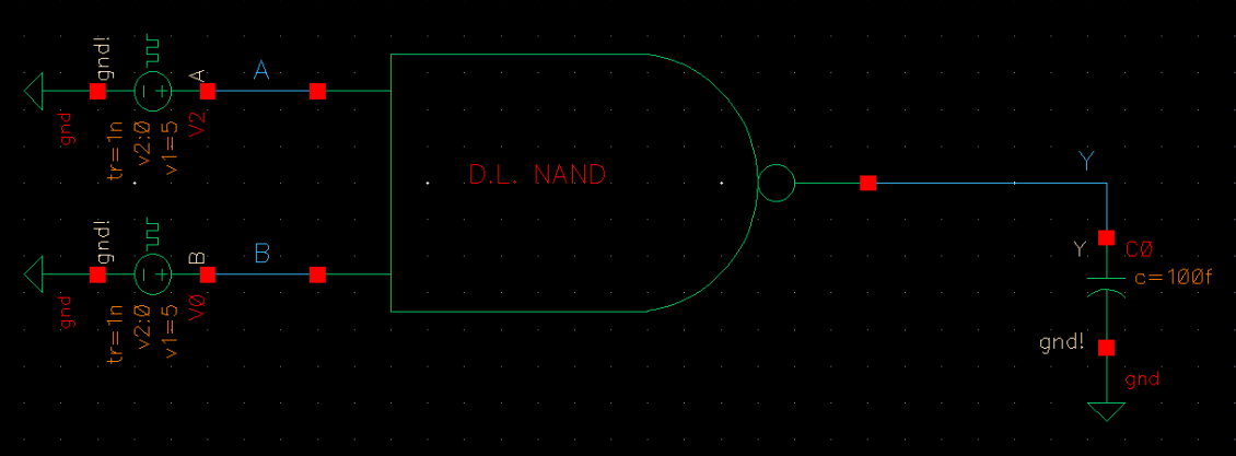
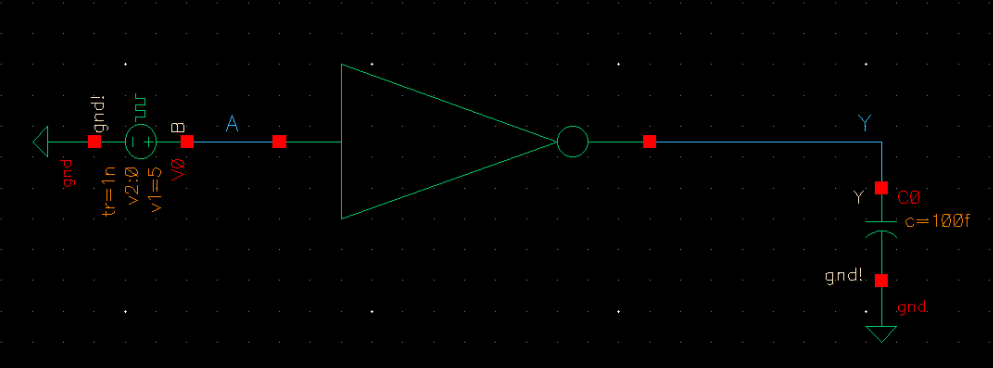
At this point, the NAND gate can undergo a simulation to verify the that the logic
is consistent. The following schematic is used to test the NAND gate by using
a transient simulation.
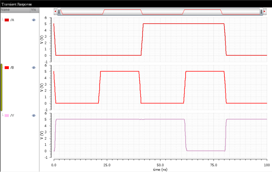
Here are the results of the simulation.
Lab
Inverter:
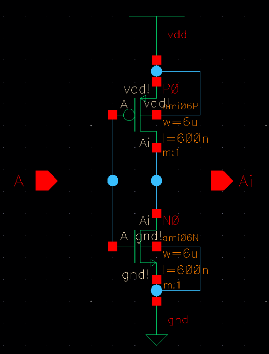
The next building block needed is a 6µm/600nm inverter.
To speed up the process, the inverter from lab 5 is copied and modified. Here is the schematic and layout.
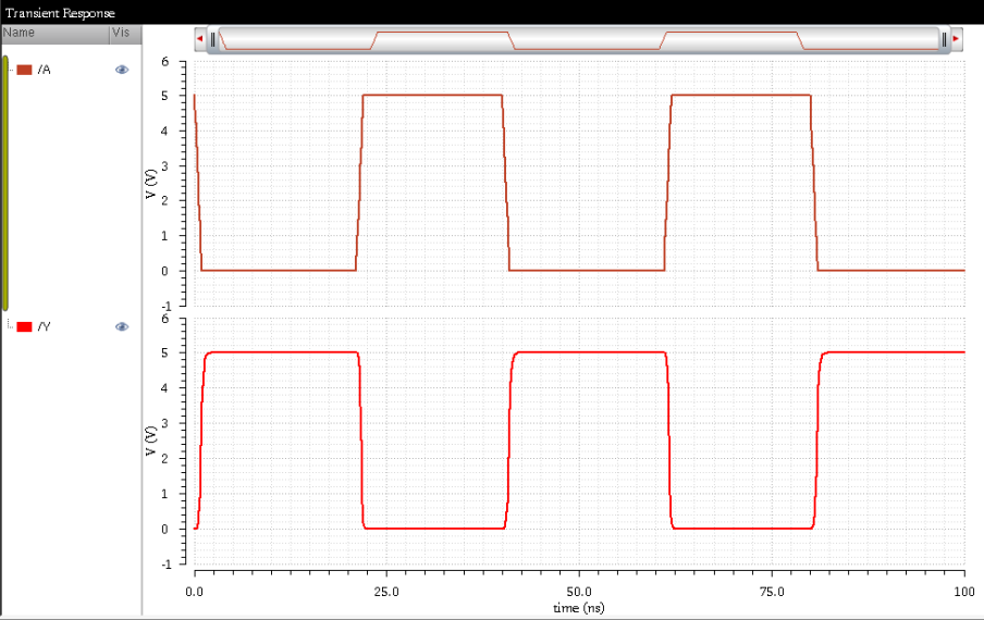
A symbol is made, and then the inverter's operation is verified through transient simulation.
Xor Gate:
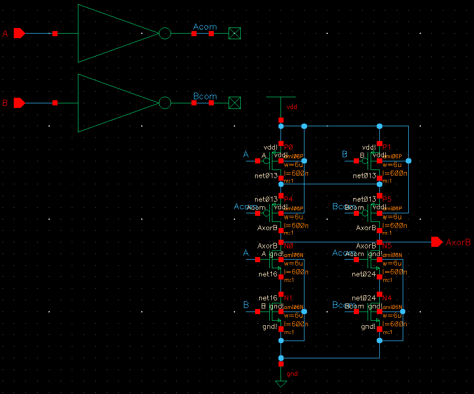
Next, we design a CMOS XOR gate, the final building block of the full adder.
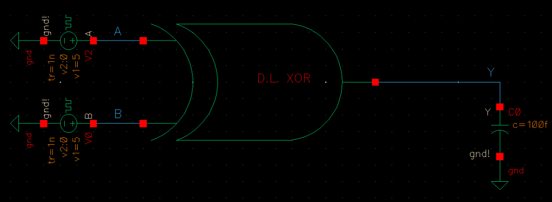
The following schematic is used to implement the XOR functionalities.
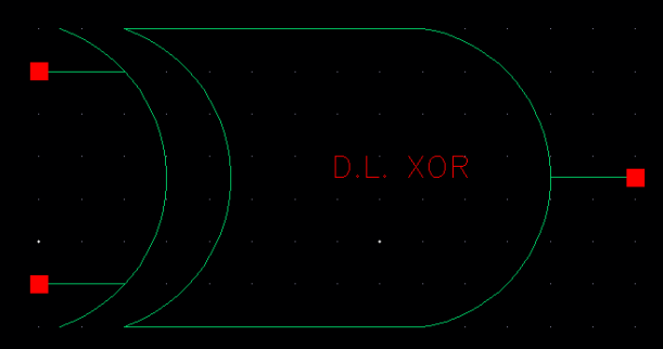
A standard symbol used for the XOR gate is made from the schematic view to be used in more schematic
level design.
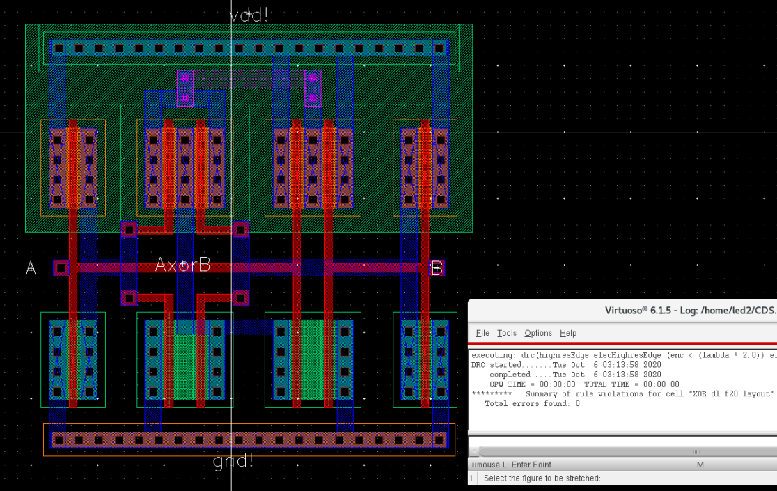
Now the layout for the XOR gate is created. Again, the layout undergoes a DRC.
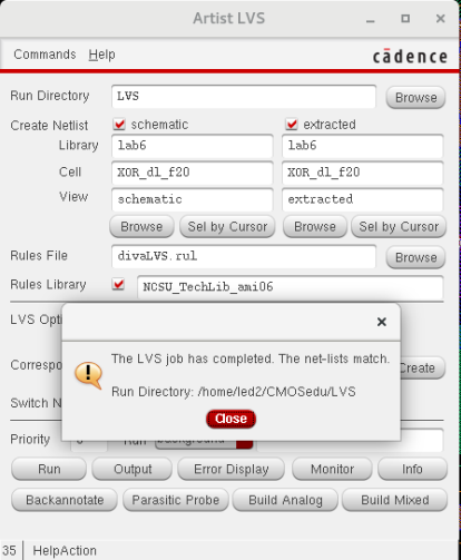
An LVS is done to verify that the schematic matches the layout.
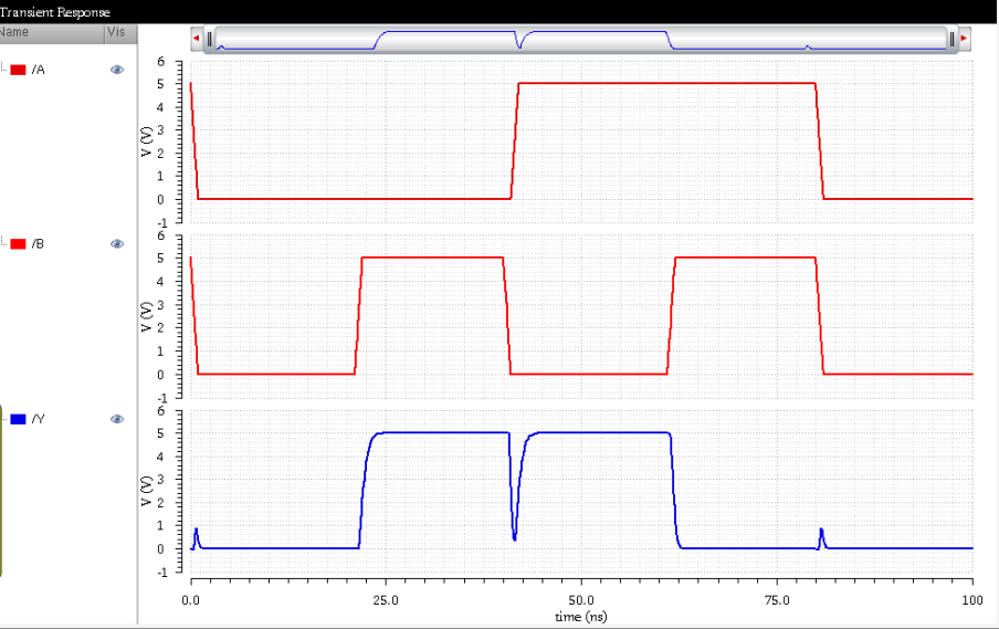
Now a simulation is done to verify the function of the XOR gate.
The waveform shows the XOR gate logic table as expected.
Full Adder:
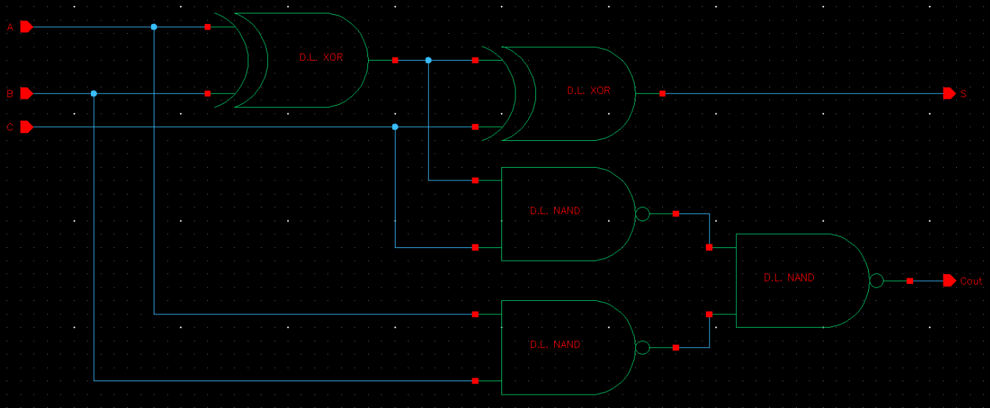
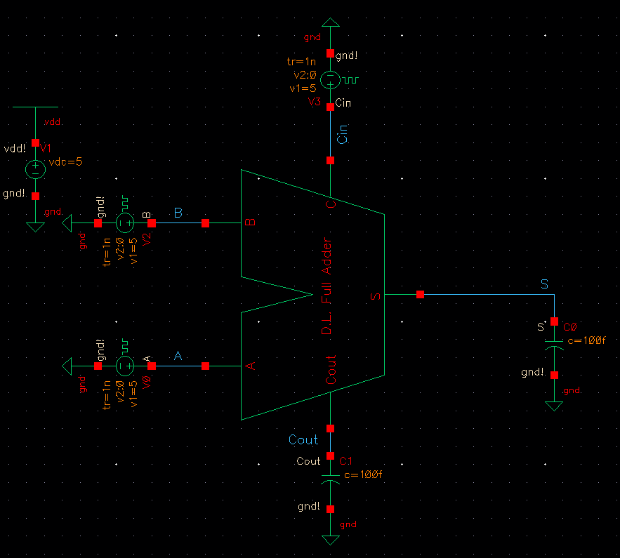
Now the building blocks for the full adder are ready. The full adder components are assembled on the schematic
level as shown below.
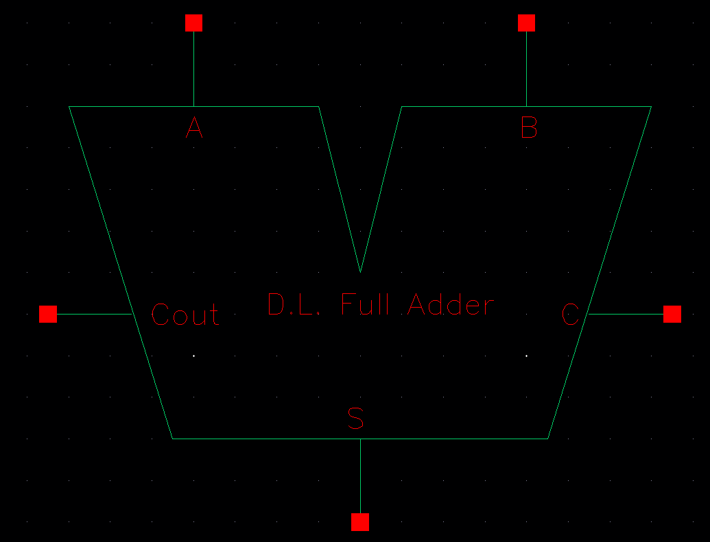
The standard symbol for a full adder is made.
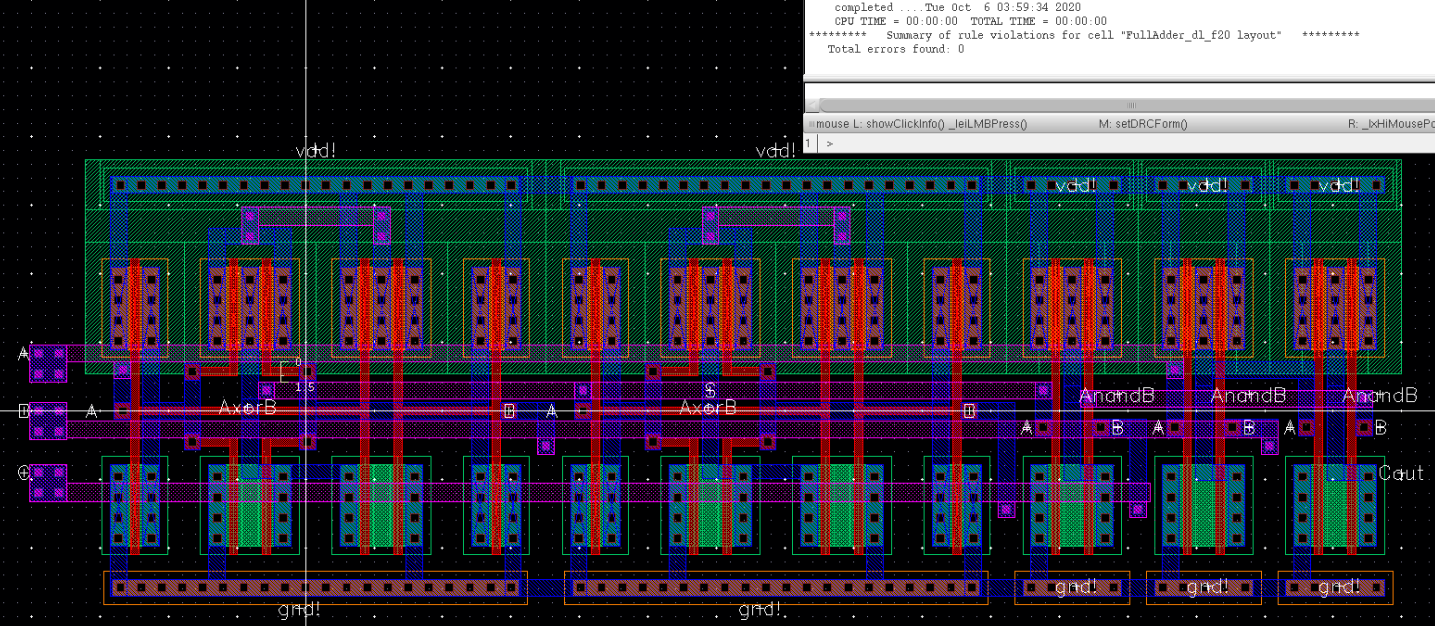
It is time to create the layout for the schematic. Each building block is instantiated and connected. This is followed by a much needed DRC.
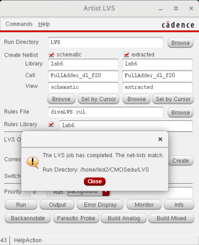
A final LVS is done to verify that the schematic and layout are consistent.
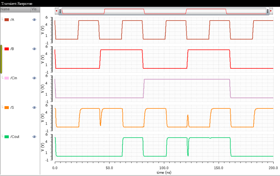
Finally, the logical functionalities of the full adder can be verified. The full adder is placed into a schematic.
Here are the simulation results.
Conclusions:
Notice, that during the simulations, there would be small glitches—peaks in voltage on the outputs.
This is likely due to either the NMOS or PMOS not yet having their gate voltage set to the correct value to
turn on or off yet as the input is still transistioning. For that reason the peaks would occur when at least one of the input is
rising/falling.
The cells for the lab can be found here at lab6_dvl.zip.
That concludes the Full Adder Lab.