Lab 3 - ECE 421L
Authored
by Do Le (led2@unlv.nevada.edu)
8th of September, 2020
Lab Description
The goal of this lab is to create the layout for the schematic of the
Digital to Analog Converter (DAC) that was
drafted last week. We start by creating the layout for a 10kΩ n-well resistor, and then working from there.
Prelab
Back up the work done in lab 2.
Lab
Resistor:
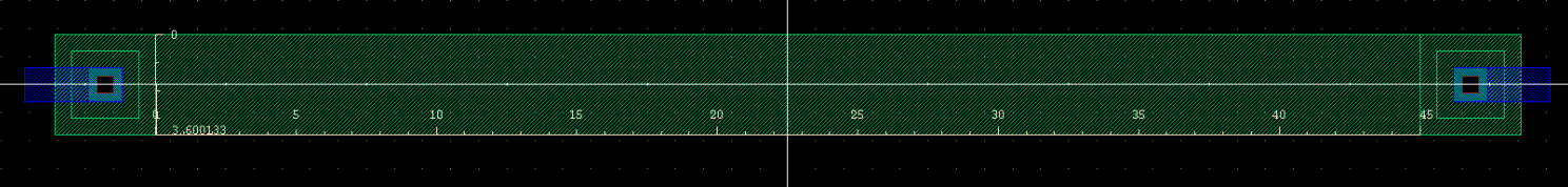
We start the layout by drafting a layout of a 10kΩ n-well
resistor. Using a sheet resistance of 800Ω/square,
we can design a rectangular resistor. For our process, we will use a lambda of 0.3µm.
The minimum width of the n-well allowed as defined by the MOSIS design rules is 12*lambda or 3.6µm.
Using a width of 3.6µm, we can
calculated the length of the resistor necessary
for a 10kΩ resistance. The resistance is calculated as R = r(L/W) where
R is the total resistance, r is the resistance
per square, L is the length, and W is the width. It follows that L = (R/r)*W = (10kΩ/800Ω)*3.6µm = 45µm.
We can then draw our n-well resistor, and place an ntap cell at the ends to connect to the metal1 layer.
To verify that the widmth and length matches our specifications, we can use the ruler by pressing the
hotkey 'K'.
To verify that the resistor fits the MOSIS design rules, we perform a DRC.
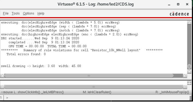
Now we can extract the resistor, and show it's value.
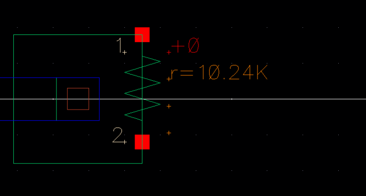
Resistor Module:
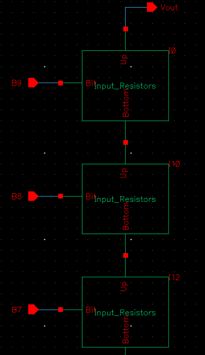
Now we move on to building the layout for the modules that were
connected to create the DLC. Recall that the module's
schematic is the following.
We instantiate three of the n-well resistors. We keep the resistors
parallel to each other in the layout view,
and connect them to match the schematic view by use of the metal1 layer.
The pins are then placed on the proper nodes.
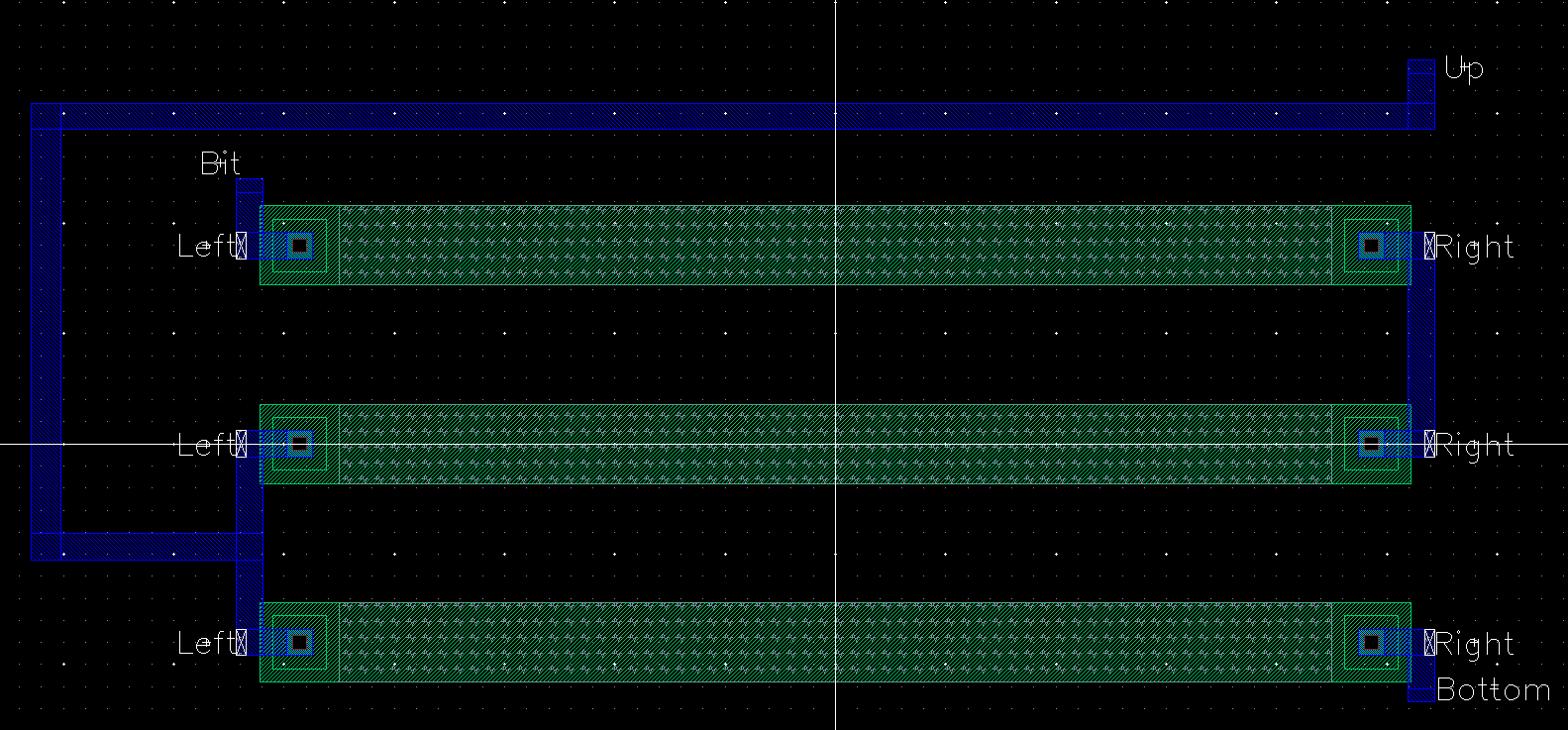
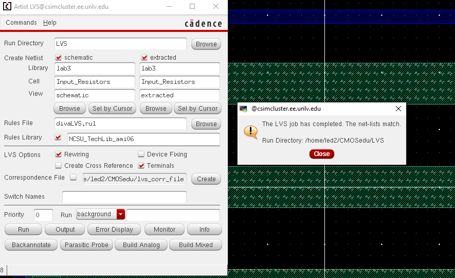
After another DRC, we can perform an LVS to verify that the layout matches the schematic.
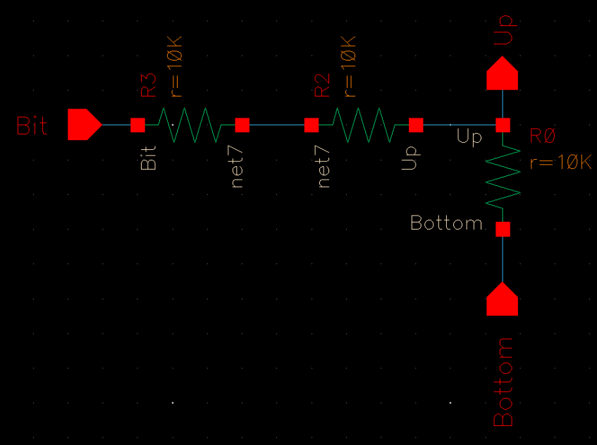
DAC:
Now we are ready to layout the DAC. Recall that the schematic for the DAC at this point chains 10
resistor modules together like so:
We instantiate 10 of the resistor modules in a layout view and connect them like so:
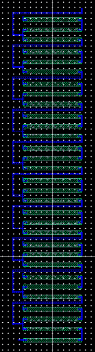
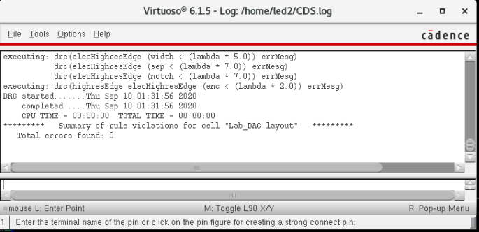
Now we are almost done with the layout. We verify the DRC passes...
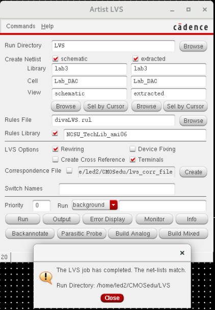
We then verify the layout matches the schematic for the DAC with a final LVS.
And that concludes the layout of the Digital to Analog Converter Schematic that was drafted
in lab2.
Return to led2 lab directory