Lab 2 - ECE 421L
Lab Description
The purpose of this week's lab is to analyze and design a 10-bit digital to analog
converter. The DAC converts a digital binary number to a corresponding analog
output signal. In the lab, we will design a DAC using n-well resistors.
Prelab
Starting the prelab:
The pre-lab served as an introduction to ADC and DAC.
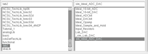
To start the pre-lab, I downloaded the following ADC and DAC cell
The lab2 cell can be downloaded on the lab page here.
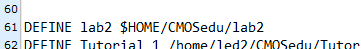
I made sure to add "DEFINE lab2 $HOME/CMOSedu/lab2" to the "cds.lib" file.
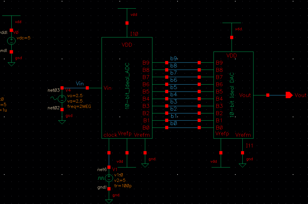
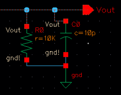
Shown here is the schematic and graph for the cell highlighted above.
Simulations:
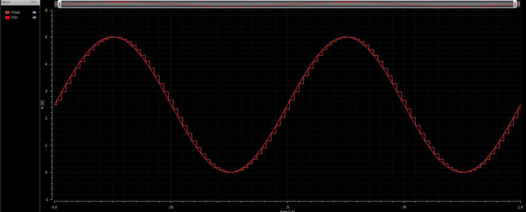
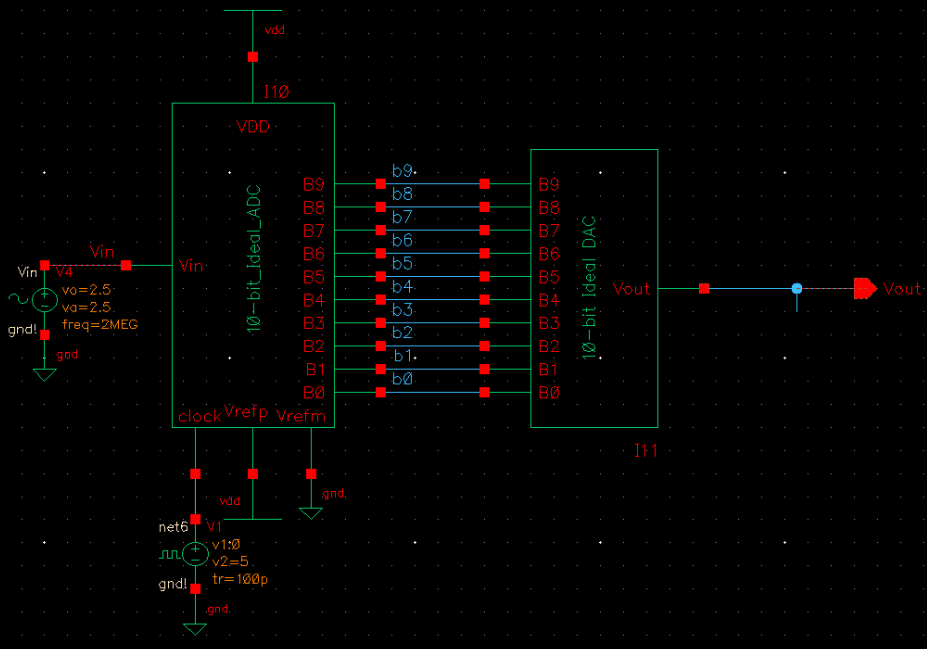
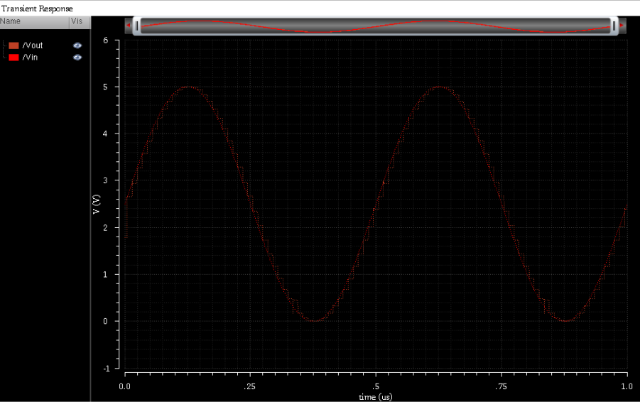
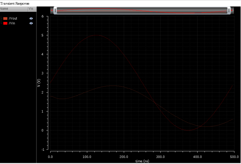
I then simulated the schematic, analyzing the input voltage and output voltage on the same graph.
For the circuit, the voltage Vin is converted to a digital integer stored in the bus B[9:0], by use of the Analog-to-Digital converter seen to the left.
Lab
The goal of the lab is to design a 10 bit Digital to Analog converter based on the following design.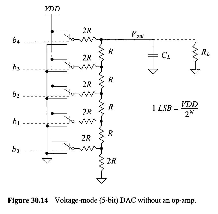
DAC Design:
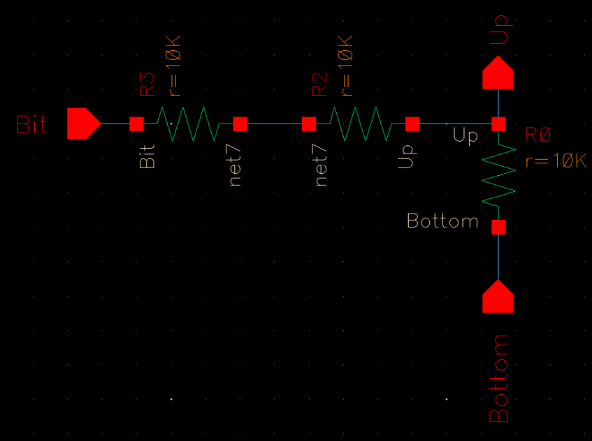
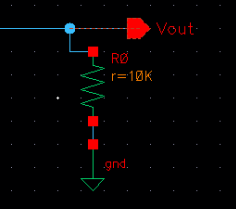
To make the design easier to analyze, I started by making a module that includes a section of the resistor
combination. This is done on it's own cell, which I called "Input_Resistors". Shown here is the schematic of the cell.
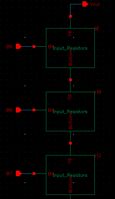
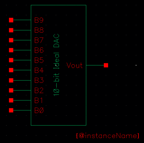
In a different cell, I then connected the modules together to create the 10-bit DAC as shown here.
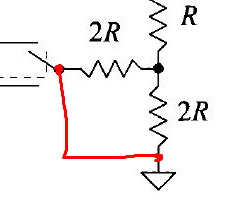
The resistor then combines in series with the one just above, and the equivalent resistance is once again 2R. This
is done iteratively until the network reduces to a single equivalent resistor of value R.
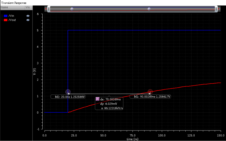
Delay:
If the DAC is driving a capacitive load of say, 10pF, the delay (defined as time it takes to reach half the output value in steady state),
is 0.7RC.
We can test this by observing the delay time when the bit B9 is at 5V and the other bits are grounded. In which case Vout is 2.5V in steady state
(there is a voltage divider in this configuration).
In our case the delay time will be 0.7(10kΩ)(10pF) = 70ns. It will take 70ns to reach Vin/2/2, or 1.25V (the delay is time to reach half the steady state voltage).
The delay can be viewed in the simulation here.
Creating a Symbol:
Simulation:
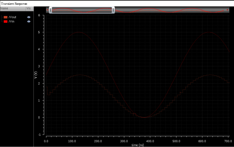
Now we are ready to simulate the operation of our newly created DAC. First, we simulate the output voltage
with an open as the output. The ADC operates as expected. Here are the results.
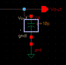
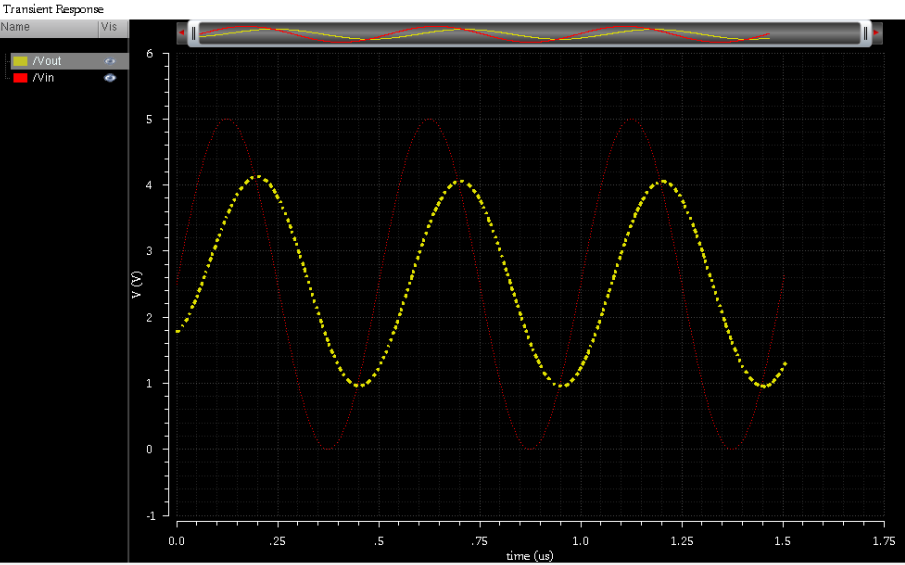
Now we see what happens when the DAC drives a capacitive load. As described earlier, there will be a delay associates
with the output waveform.
Finally, we observe what happens when the load is an RC.
MOSFET Switches:
In a real circuit, the switches in figure 30.14 are implemented using MOSFETs. MOSFETs have an associated resistance.
When the resistance of the MOSFETs are not small compared to R, the resistance is in series with the 2R resistor conencted
to each bit. This causes a larger voltage drop, which in the long run lowers the output voltage.