Final Project - EE421L
Authored
by Rhyan Granados
Email: granar1@unlv.nevada.edu
11/18/20
Project Objective:
We
have been tasked with designing, laying out, and simulating a
high-speed digital receiver for input signals D and Di. We will be
using input buffers to amplify their differences since the goal of this
project is to attain a balance for optimal speed and low-power. We are
to use figure 18.23 from Dr. Baker's book as a base design for our
circuit. We are to demonstrate the trade-offs through sims, and have
been given a goal to achieve:250 Mega-bits/sec (bit width of 4ns),
input voltage difference of 250 mV( ex. swinging between 3 and 2.75).
Finally we are encouraged to experiment with the number of inverters,
and draft a table to summarize our design's performance.
Pre-project:
(Note: I will be using 6u/0.6u for my NMOS and 12u/0.6u for my PMOS).
Before embarking on this
project, I will analyze fig. 18.17, 18.21, and 18.23 which is the
topology we are to model our design after.
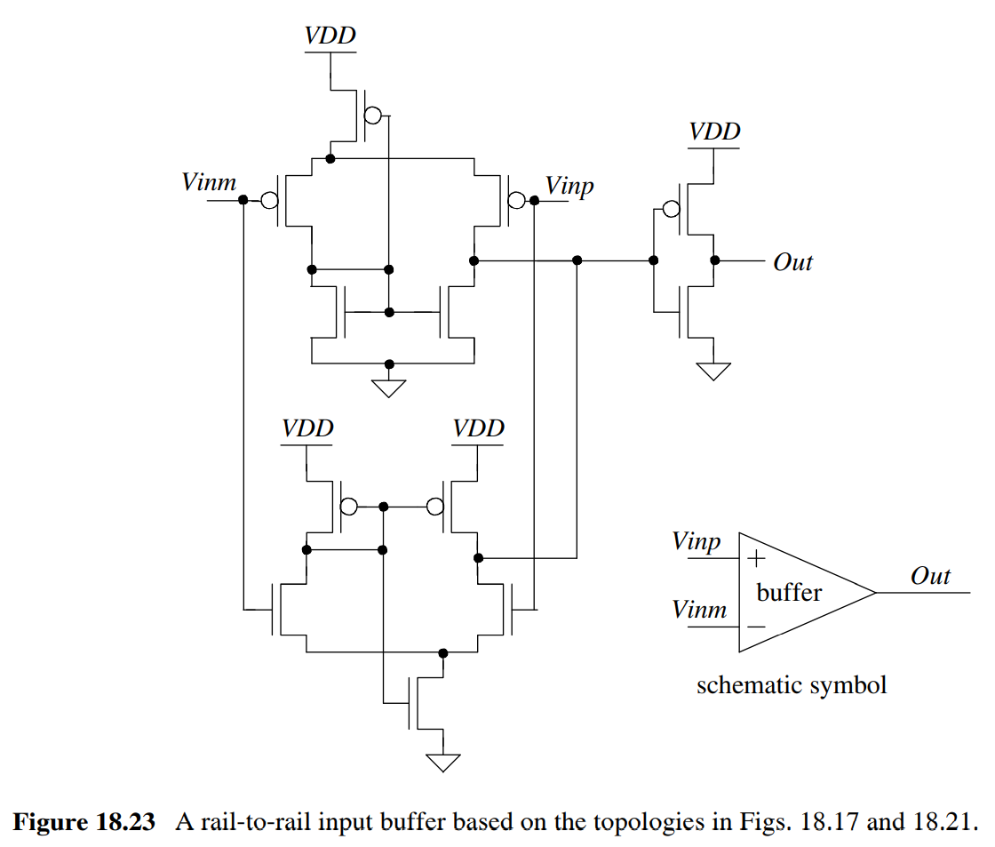
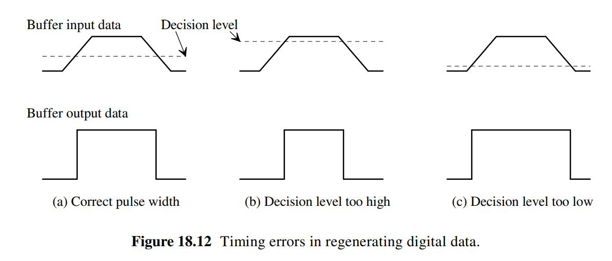
Figure 18.23 is an input buffer. Input buffers are needed in order to
decisively differentiate logic highs and lows of an input signal which
may be flawed(slow rise and fall times). A proper input buffer should
slice at a level that is neither too high or too low in order to get
the right pulse width as depicted in figure 18.12 (Baker 541). An input
buffer amplifies the difference between the two inputs D and Di.
How do you "slice" the input data?
To begin with, there are two ways to do this: "a reference voltage may be
transmitted, on a different signal path, along with the data. Alternatively, the data may be
transmitted differentially (an input and its complement)" (Baker 543). As the project objective states, we will use the second method because we are using an input buffer.
The theory is fairly simple: if D>Di then output is "1" or high
if D<Di then output is "0" or low
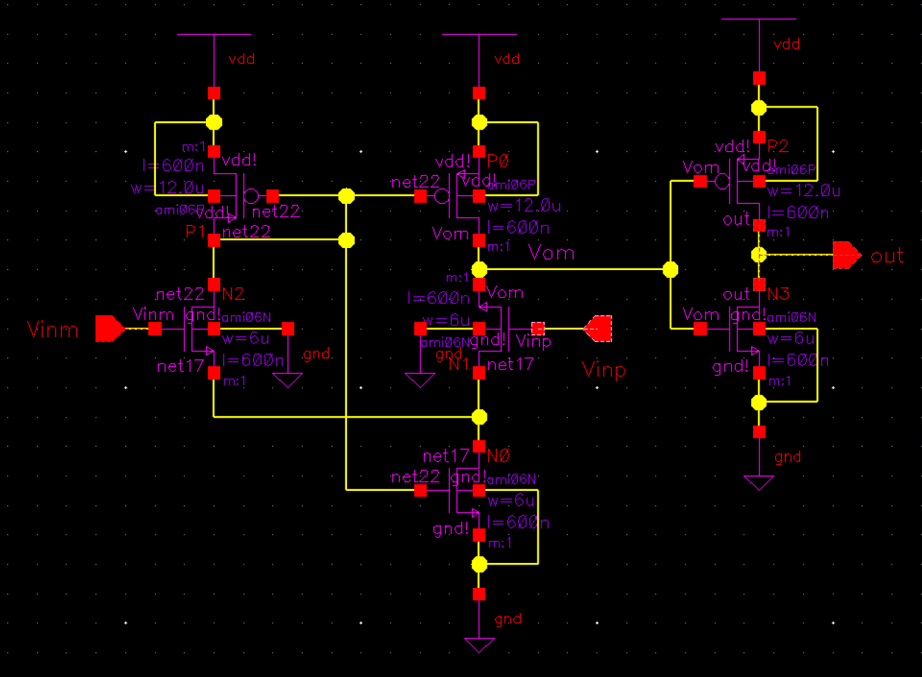
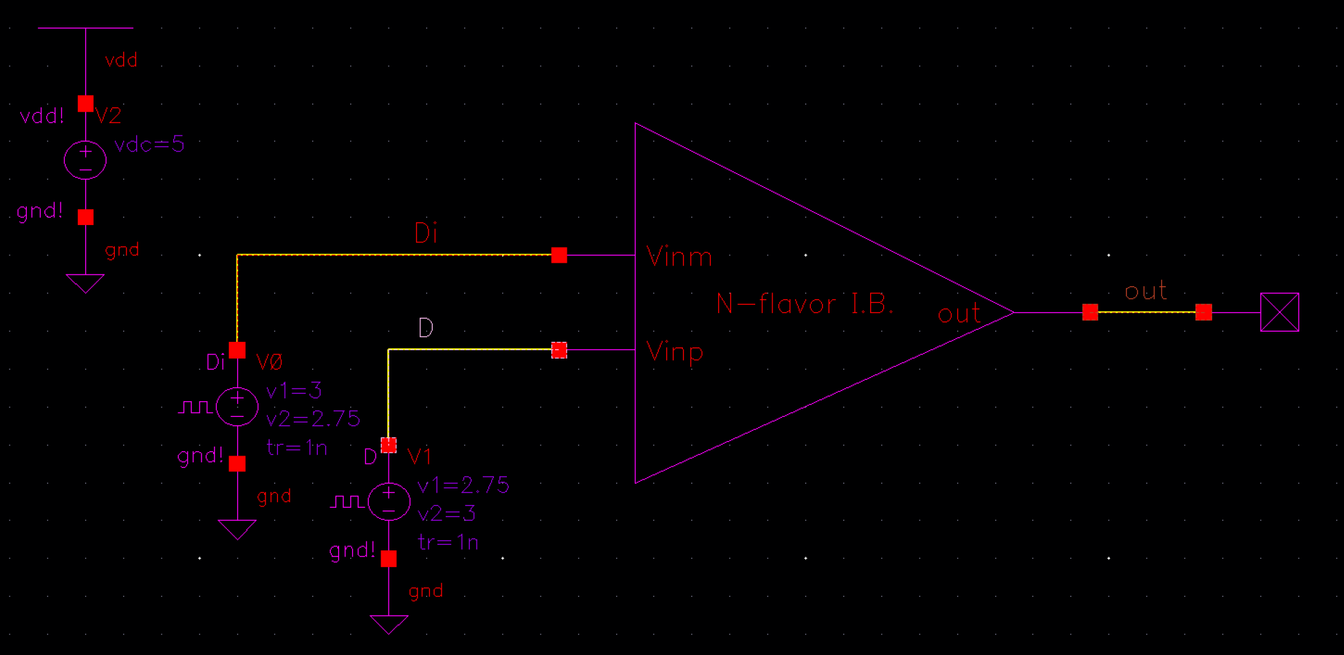
Above is a schematic view of Figure 18.17 from (Baker 544) which is an N-flavor "input buffer for high-speed digital design"
We will create a symbol and sim this to see how this will function as an input buffer
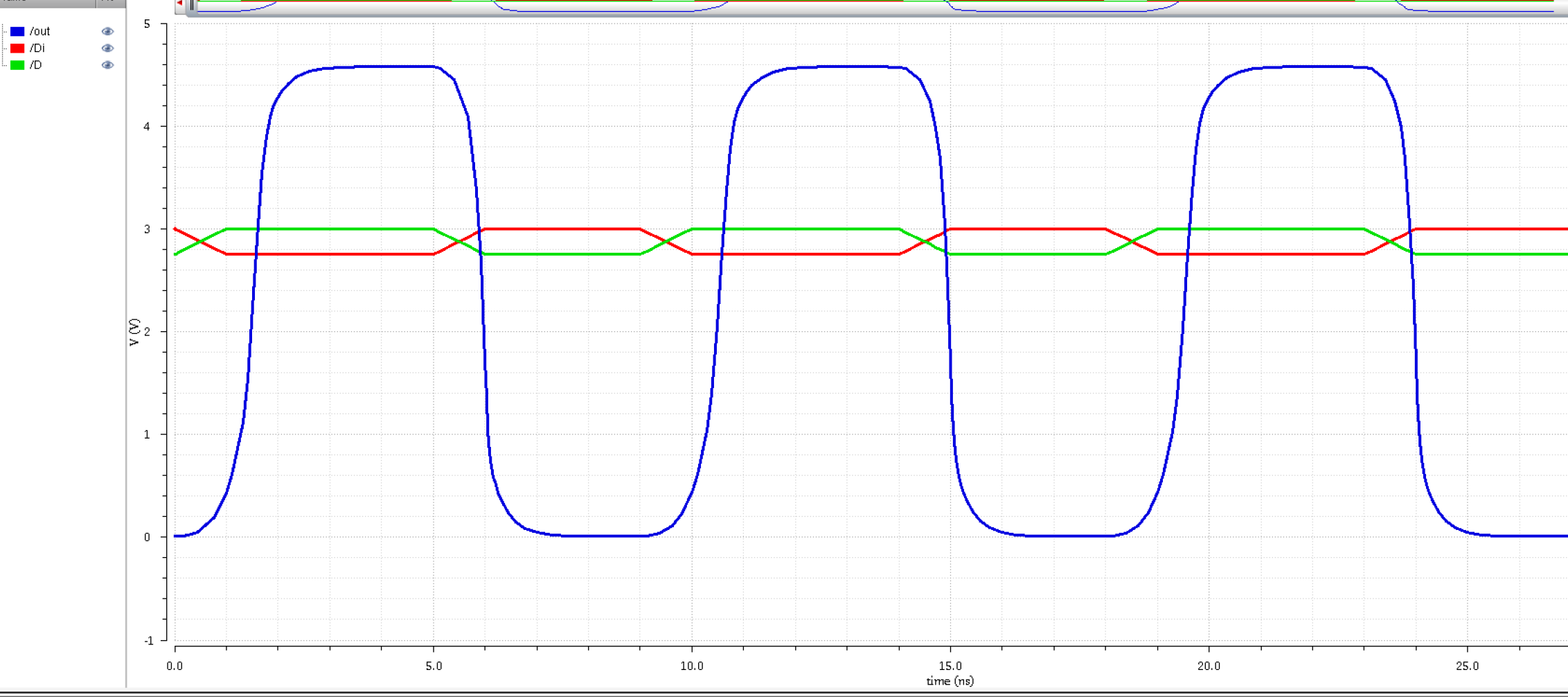
So as we can see, it functions as an input buffer but it could be
improved. The input signals are not aligned with the output signal and
the output is not fully reaching 5V(our VDD). The output could also
transition faster to make a more decisive, sharper rectangle.
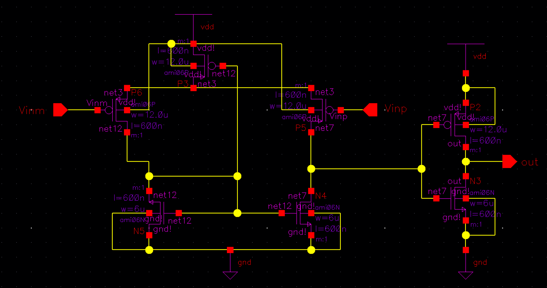
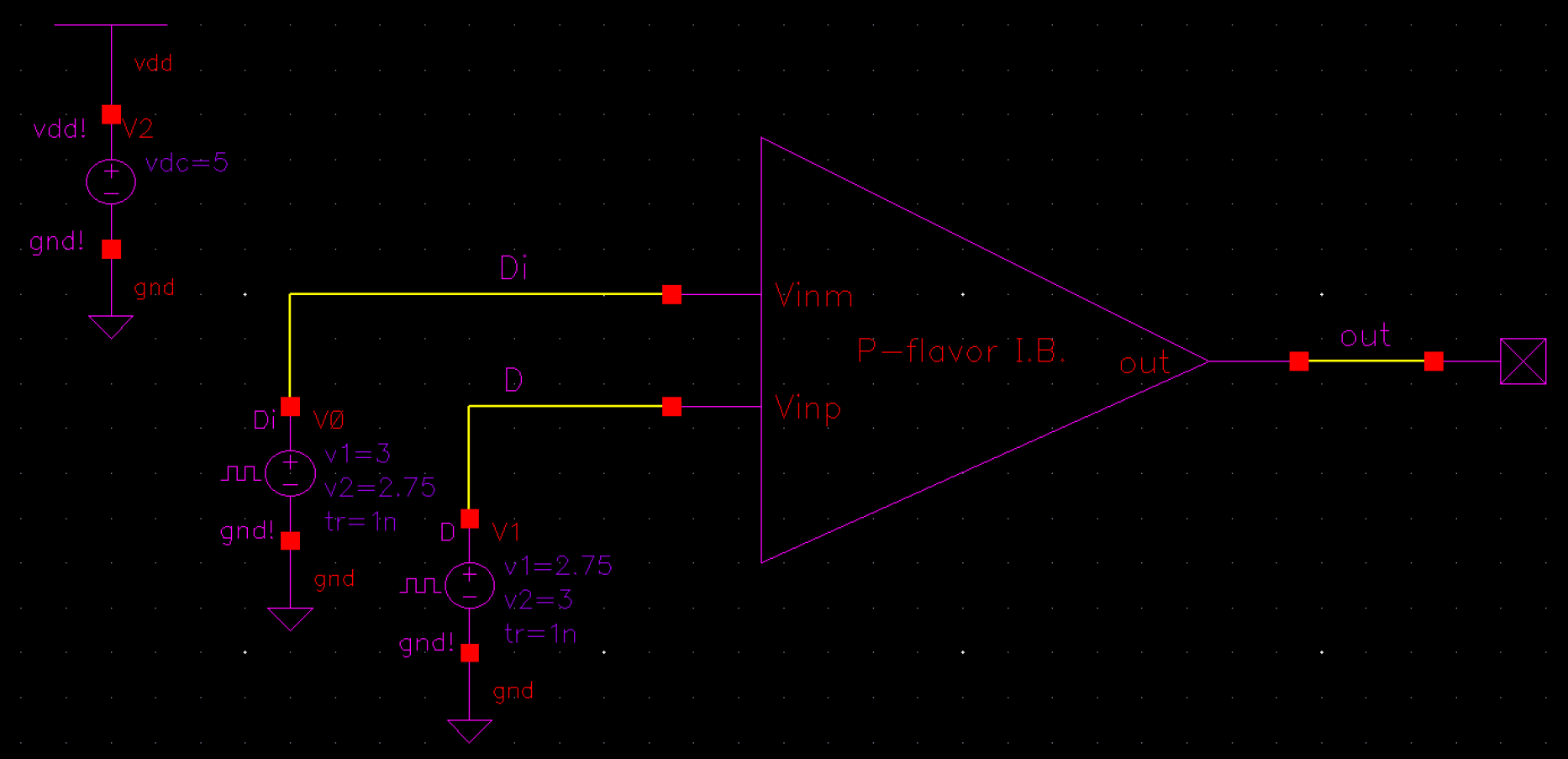
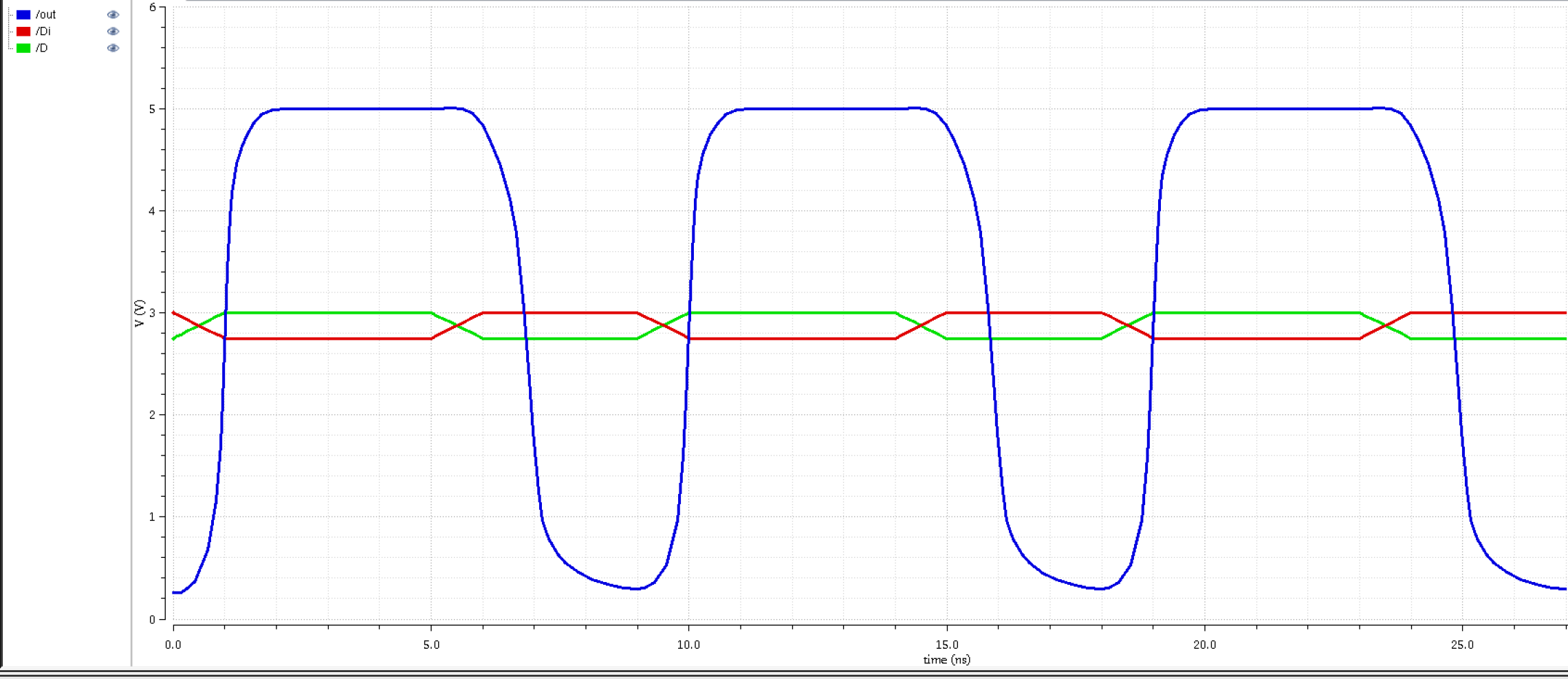
Above is a schematic view of Figure 18.21 (Baker 545) which is a P-flavor "input buffer for high-speed digital design"
As we can see, this also has its flaws, but at least the output reaches 5V(our VDD).
N. Flavor Vs. P. Flavor Input Buffer Pulse Width Comparison
N-flavor
|
P-flavor
|
The pulse widths are nearly identical, but they are still not in phase with the output.
Simulating with Higher Transitions
So, in our simulations above, I using 3V and 2.75 for my pulses, so I
was using lower transitions. I will instead use a higher transition: 0V
and 5V.
N-flavor
|
P-flavor
|
So as we can see, the N-flavor's output has now reached 5V. At higher transitions they seem to be more identical.
So we will use a higher transition: 0 and 10V. This is to see if their outputs would differ at a higher voltage disparity.
N-flavor
|
P-flavor
|
As we can see, the P-flavor is less in phase at higher voltage disparities.
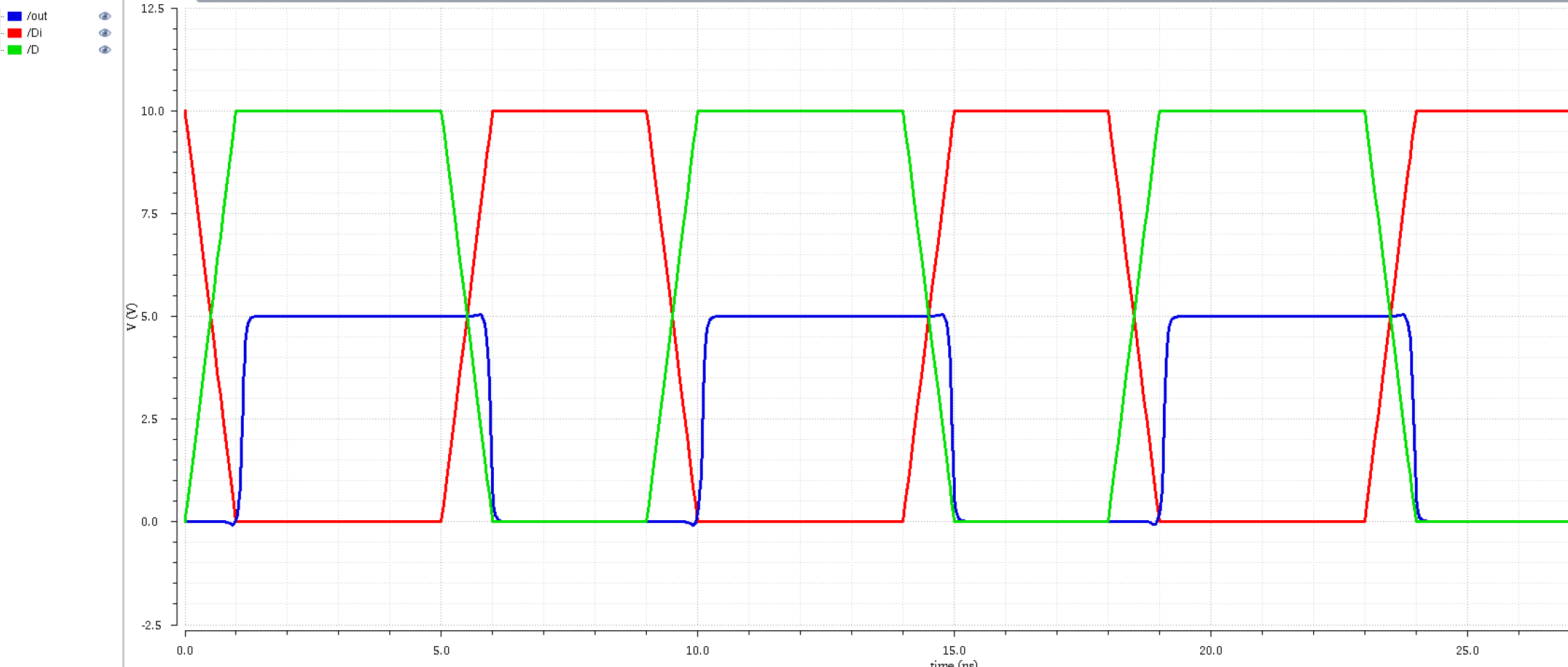
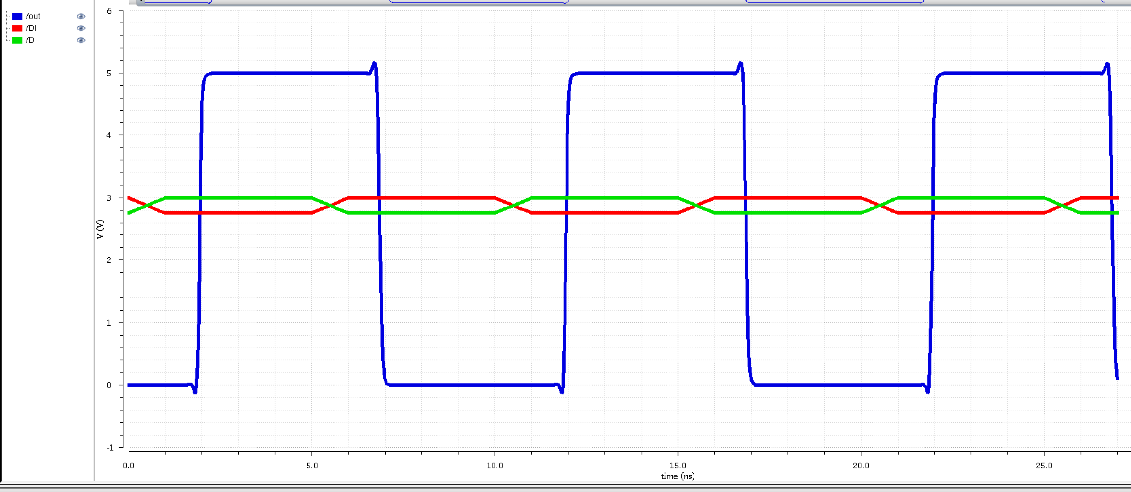
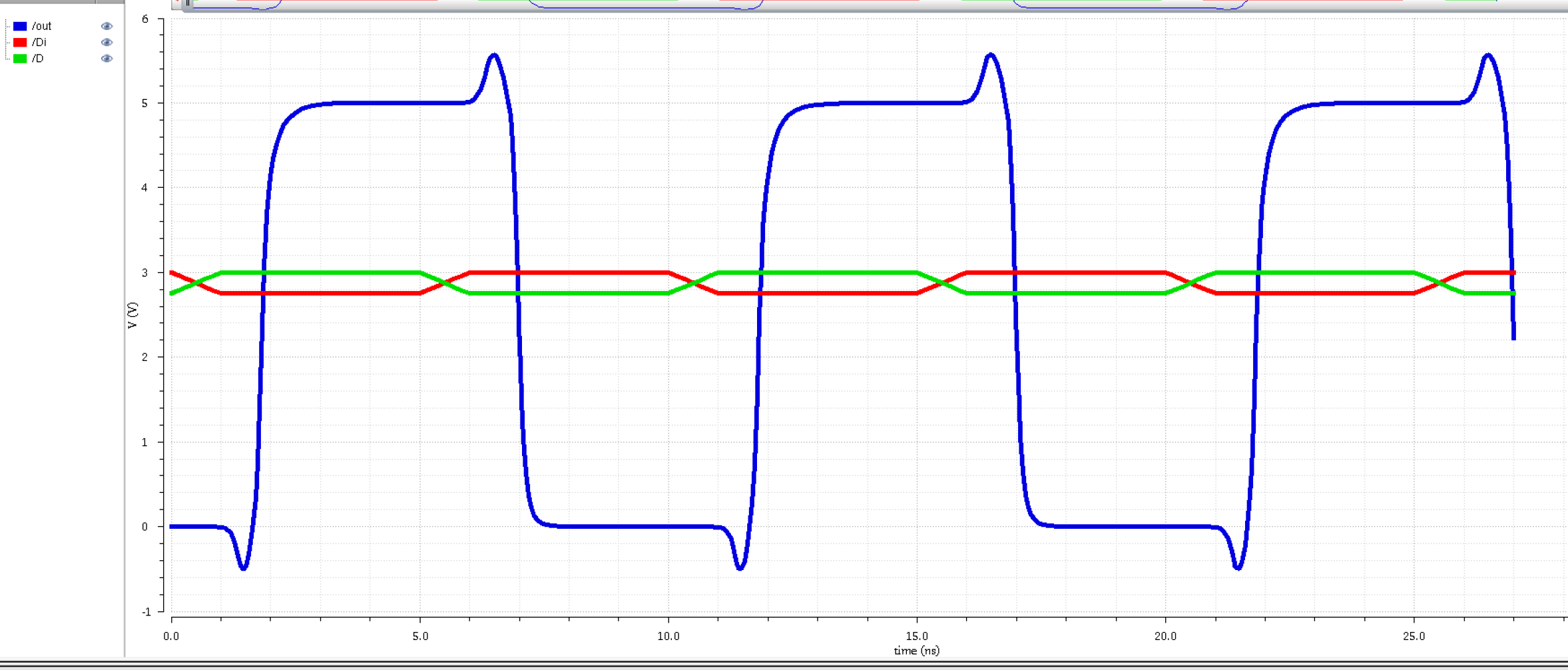
Simming Fig. 18.23
After getting a taste for
N-flavor and P-flavor input buffers, we can now appreciate Fig. 18.23
from earlier which is an N-flavor and P-flavor stacked together.
Above is the simulation results and below is a side-by-side with the descending order: N-flavor, P-flavor, and figure 18.23.
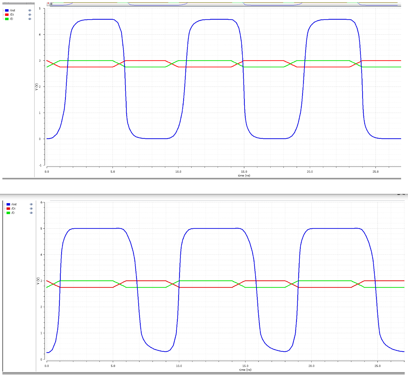
As we can see we're
getting the best of both worlds from the N-flavor and P-flavor. The
output is not quite at 5V but it's closer than if it were just the
N-flavor. The output is more concise and sharper as if it was just
N-flavor, but it also has the nice flat curve at the top like the
P-flavor. The hideous logic low output from the P-flavor is gone, the
logic high and logic low more closely resemble each other. The N-flavor
is earlier than the output by itself, and the P-flavor isn't
as early; however, it starts its low too quickly for the output to keep
up. It is now more in phase than ever. We just need to refine it a bit
more.
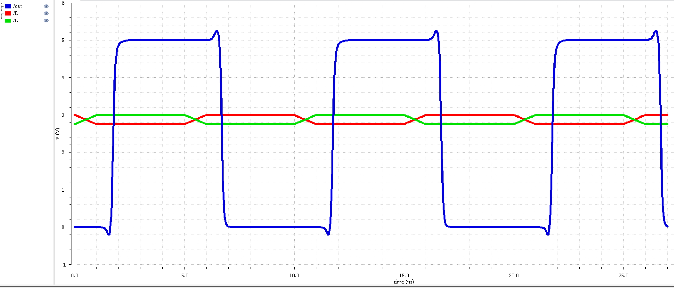
Inverters
According to the project
objective, we are encouraged to experiment with the number of inverters
at the end our input buffer. So we will do that next and observe, and
maybe it'll refine our output even more!
Note: The inverter (PMOS WIDTH/NMOS WIDTH)we'll be using for this is
6u/1.5u. This isn't final as I will try different dimensions in a bit.
This is more so to see the effect it'll have.
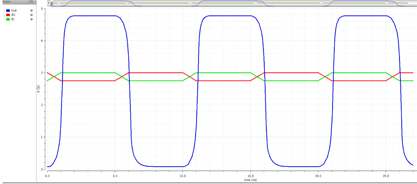
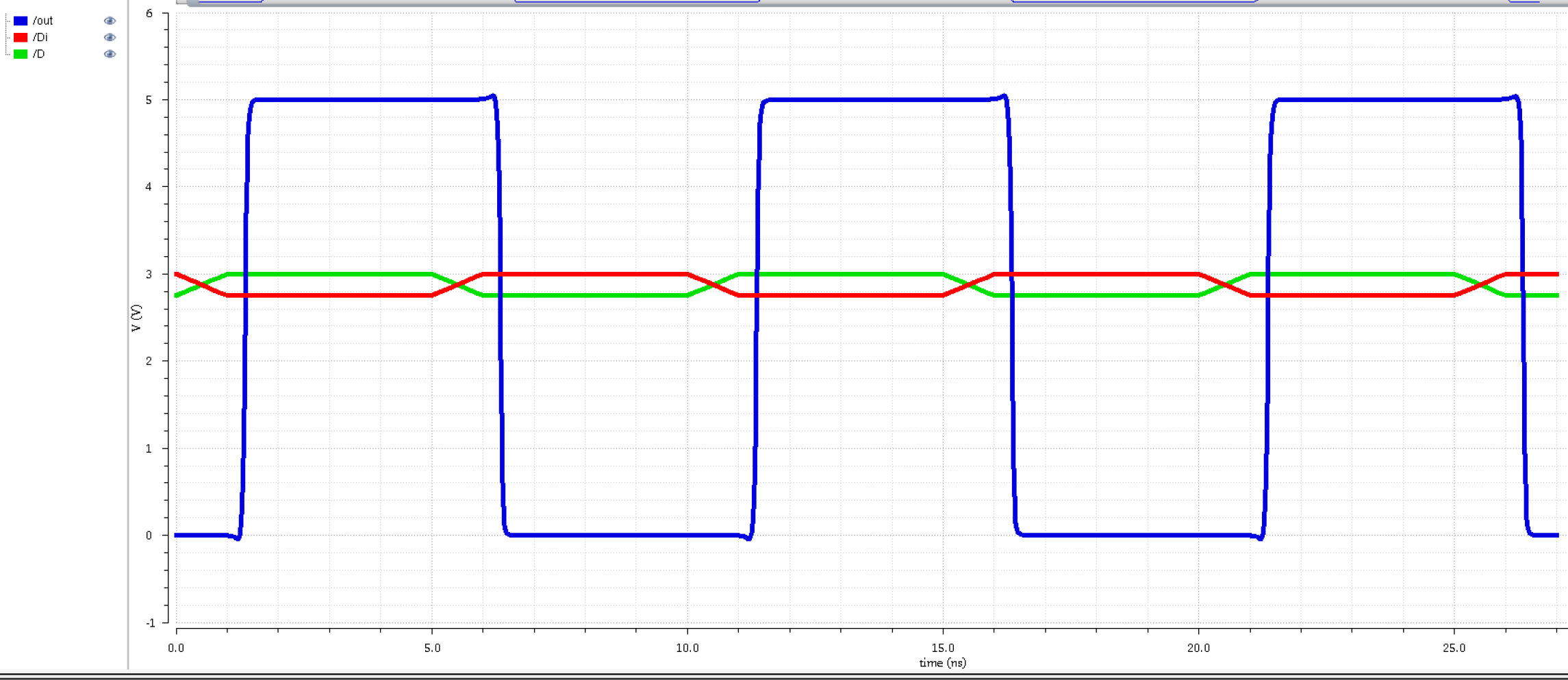
# of inverters
|
Fig. 18.23
|
2 inverters
|
|
4 inverters
|
|
6 inverters
|
|
Based on the three graphs,
having 3 buffers(6 inverters) or 2 buffers(4 inverters) won't improve
our signal that much more than 1 buffer(2 inverters). We will go with
only 1 buffer(2 inverters), this is in order to consume less power.
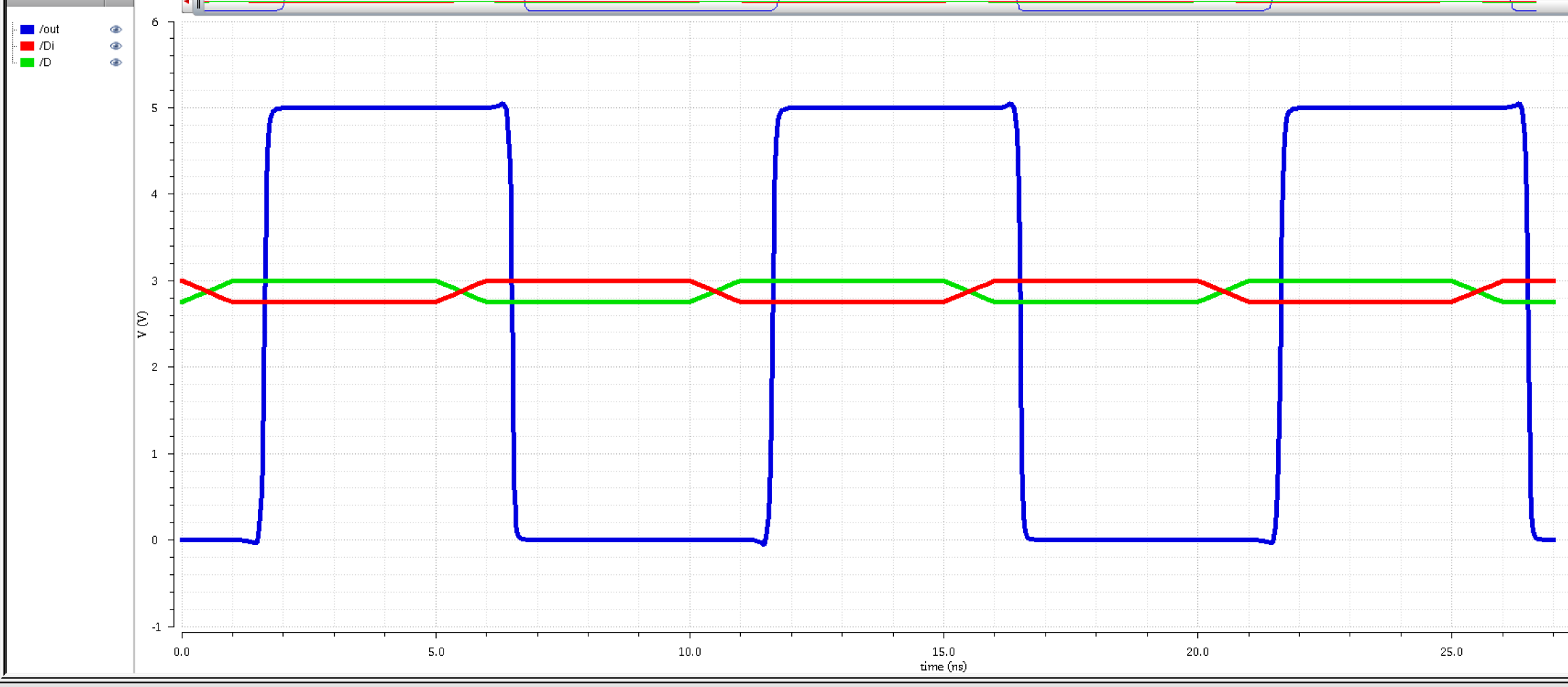
What if we add a load?
Let's add a 1 pF load to figure 18.23 after our 1 buffer.
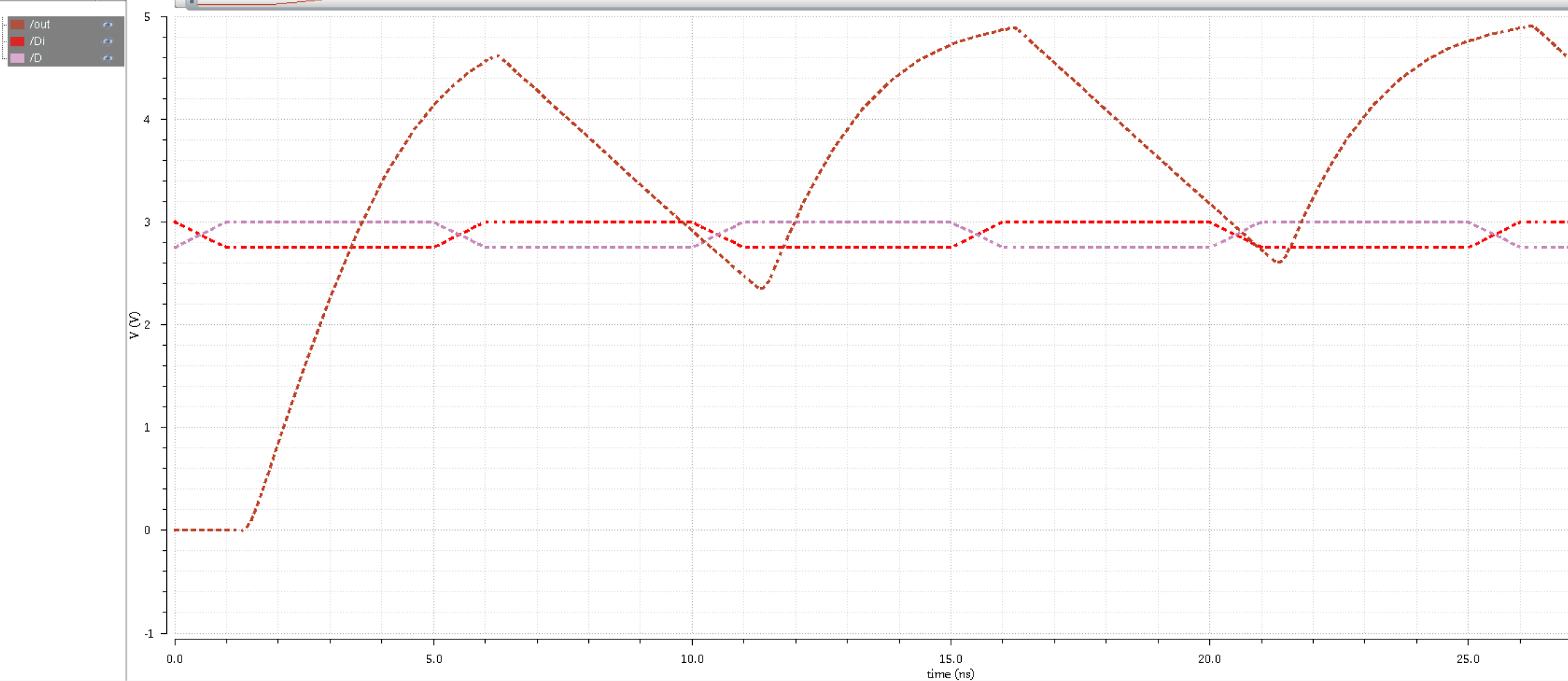
As we can see, adding a load will do us no favors.
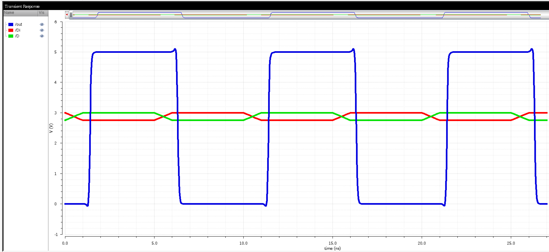
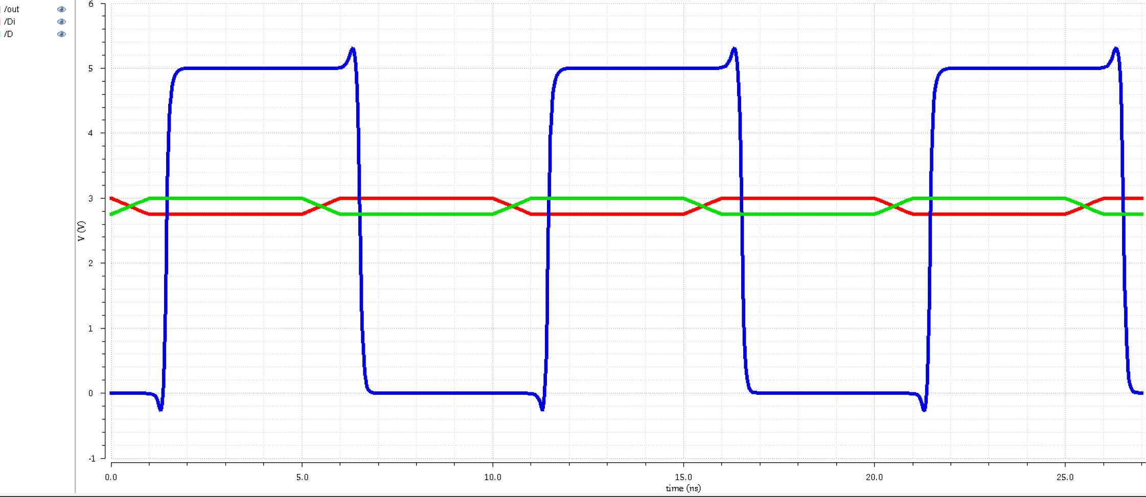
Varying the Dimensions for our Buffer
I am going to experiment with varying width and length of the inverters in our buffer
Two 12u/6u inverters
|
|
One 12u and one 24u inverter
|
|
| One 12u and one 48u inverter |
|
Two 24u/12u inverter
|
|
One 24u and one 12u inverter
|
|
One 48u and one 24u inverter
|
|
From this data sample, I am
going to conclude a couple things: 1) going up from small to big
doesn't improve our output, 2) Having two of the same bigger inverters
also doesn't improve our output, and 3) going from bigger to smaller
inverters doesn't improve our output.
With that, I'm going to keep it simple and stick with two 12u/6u inverters for my buffer.
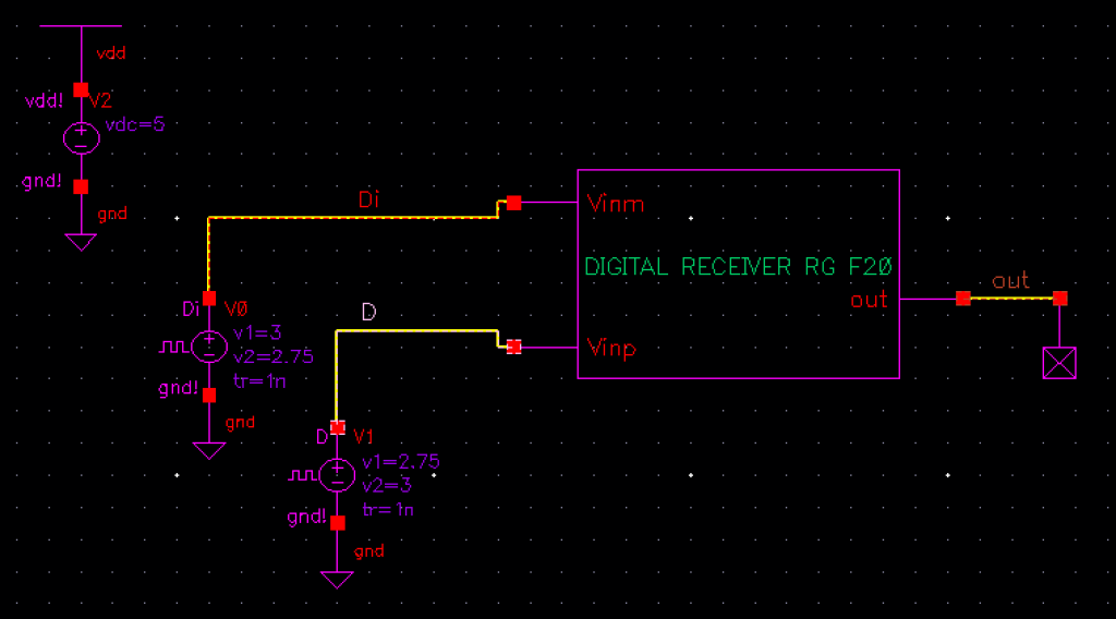
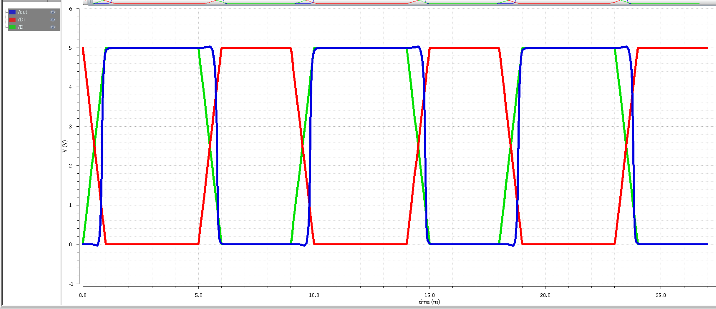
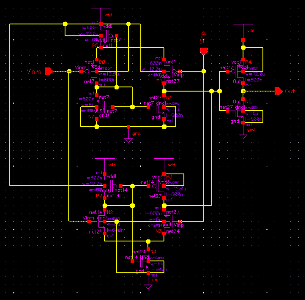
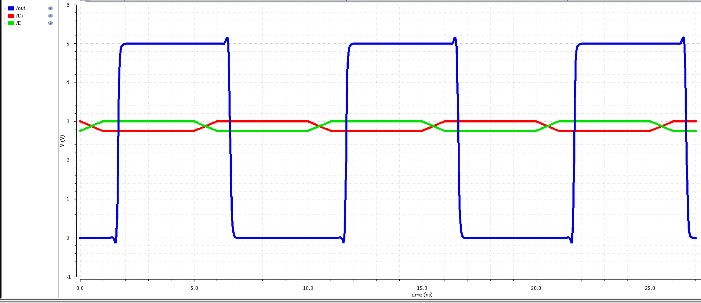
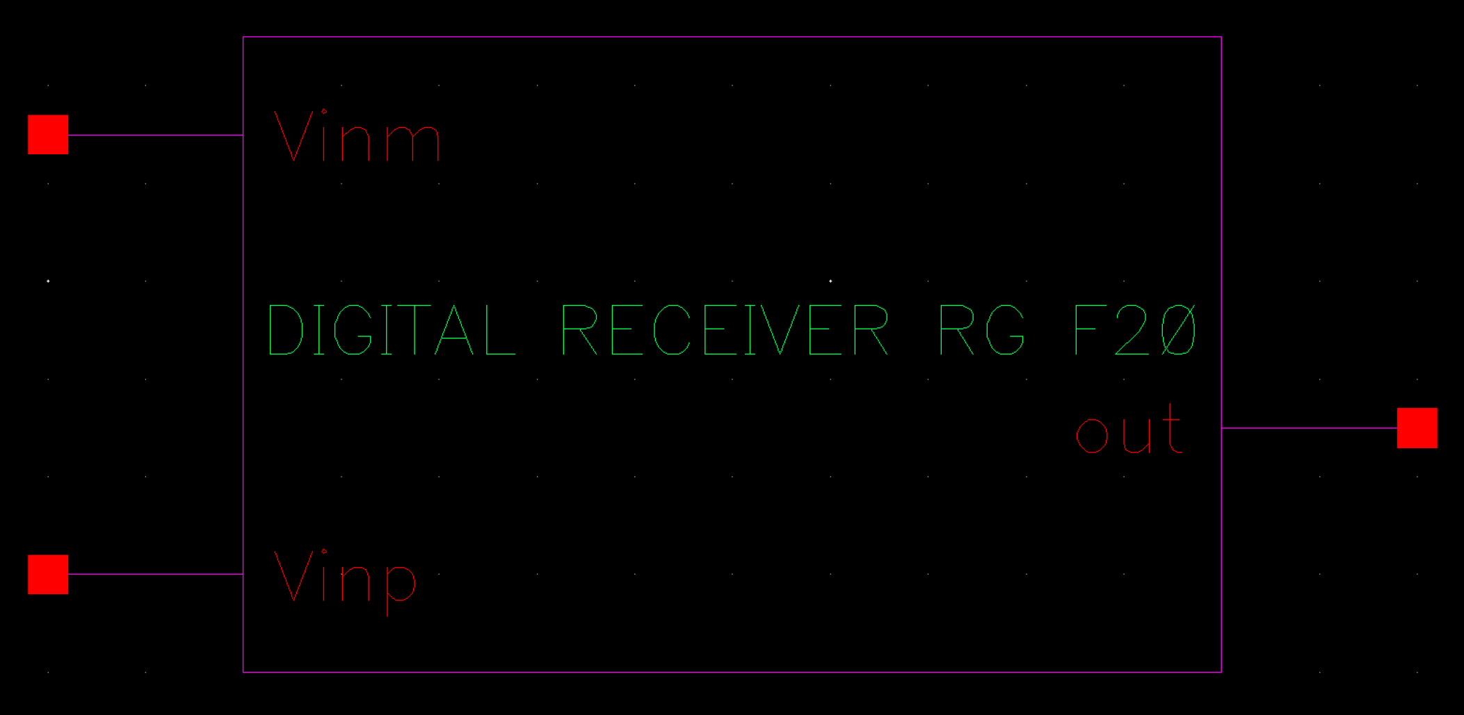
My Design:
With all the pre-emptive testing I've ran above, the configuration I've decided to go with for my digital receiver is:
Inside:
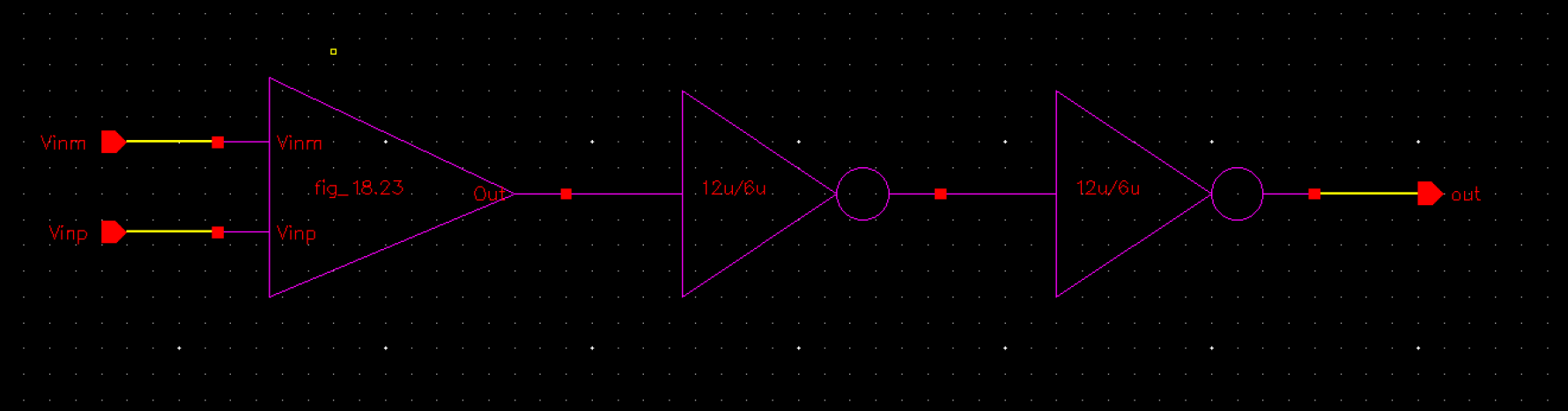
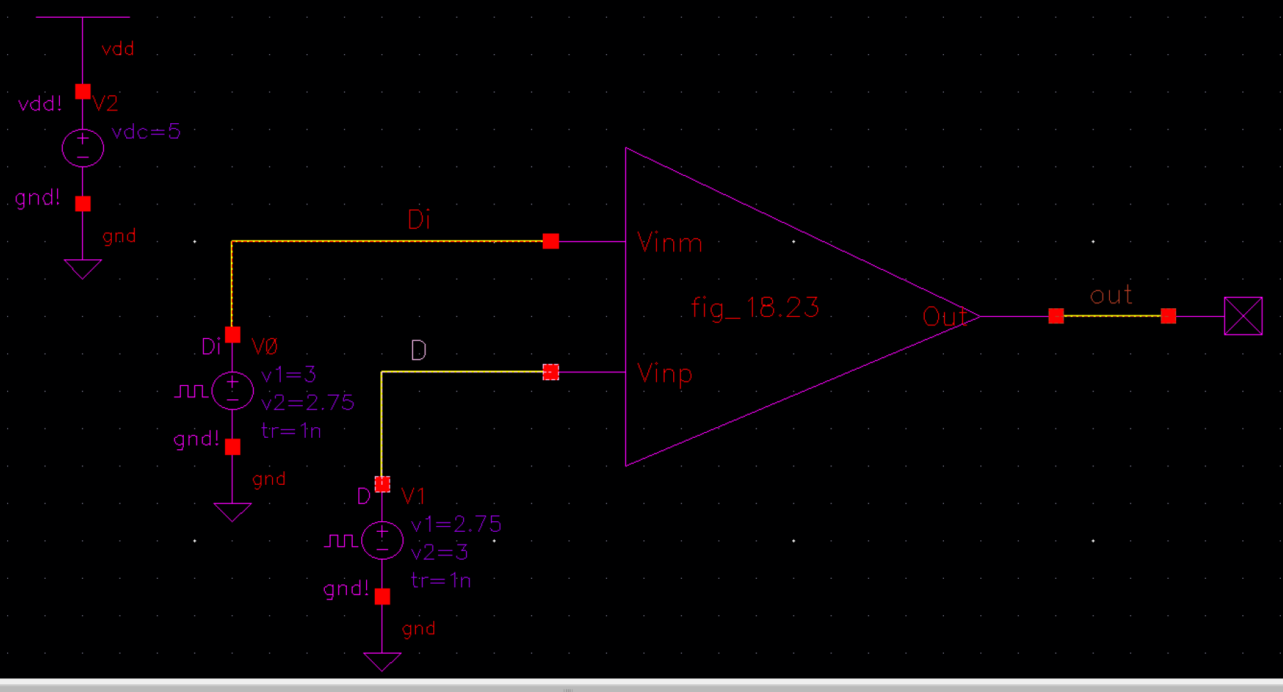
Symbol:
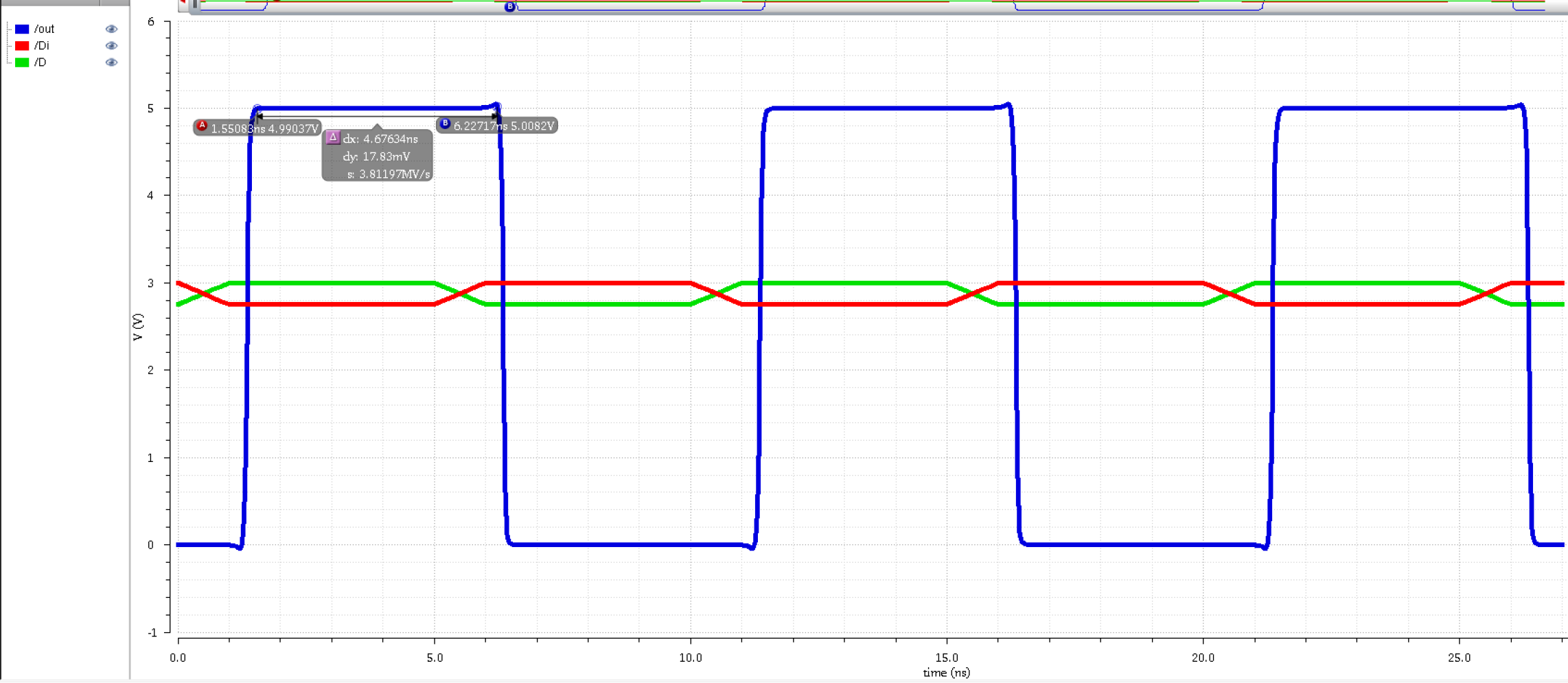
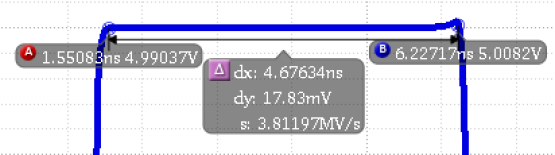
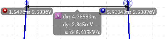
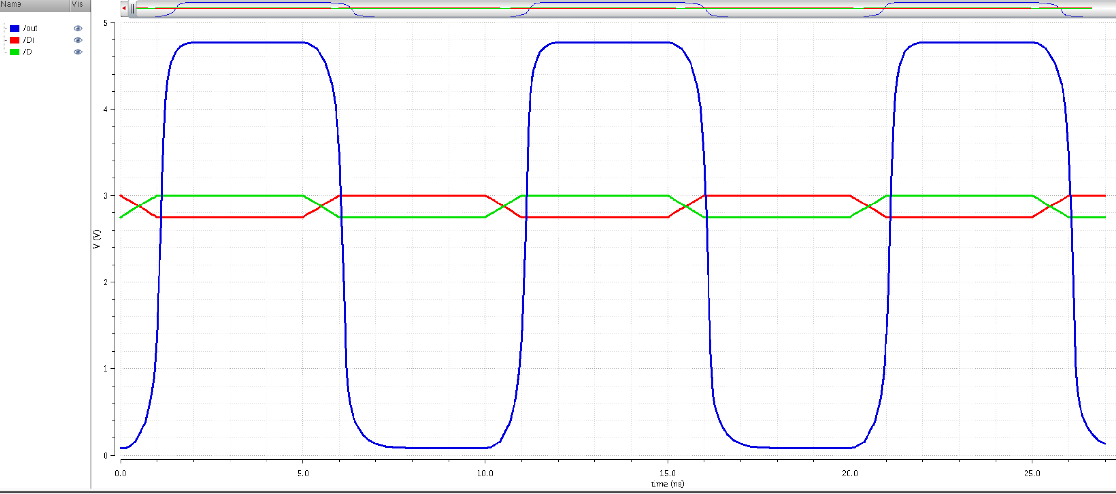
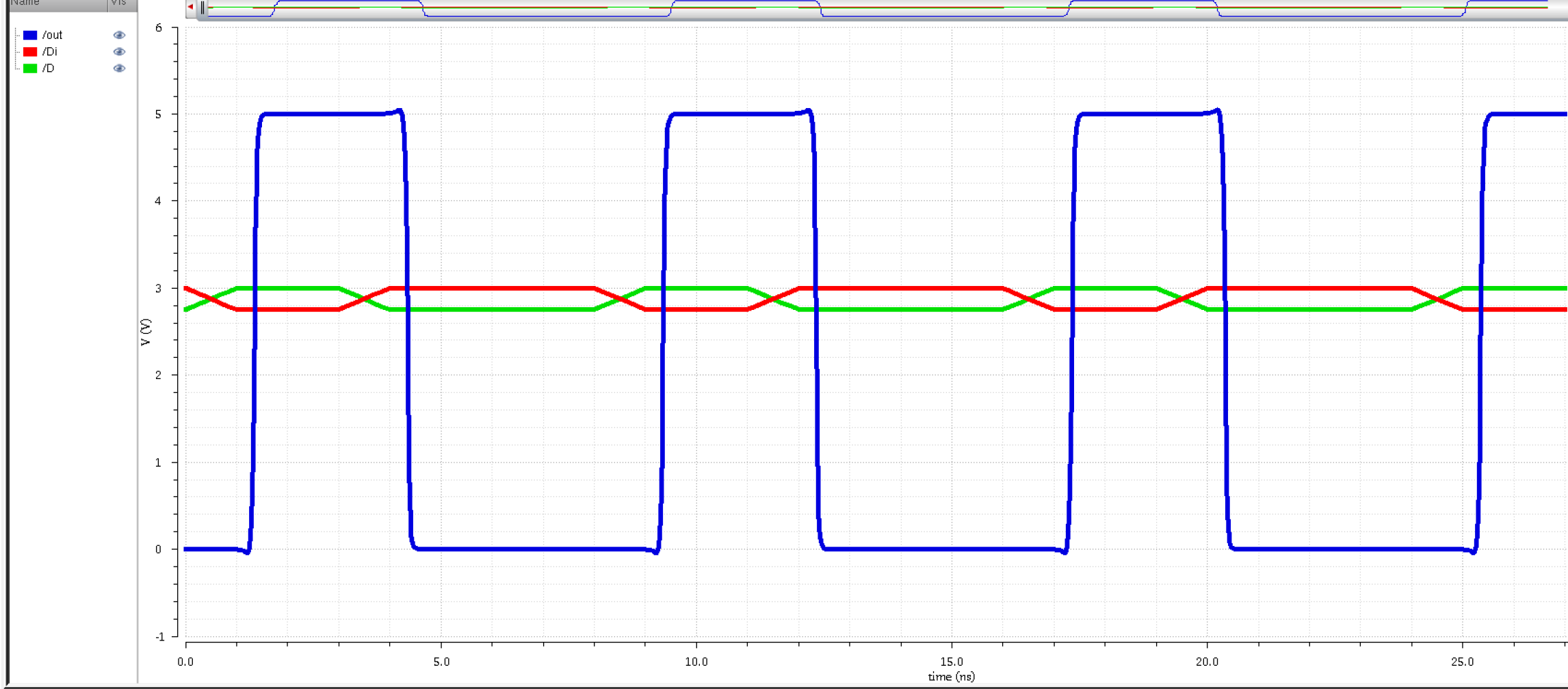
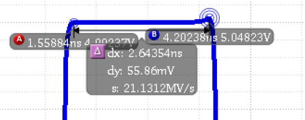
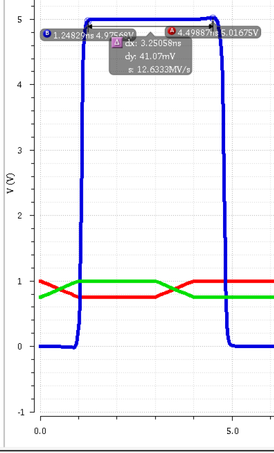
Bit-width:
The bid-with is a little over 4 ns, so it's not exact.
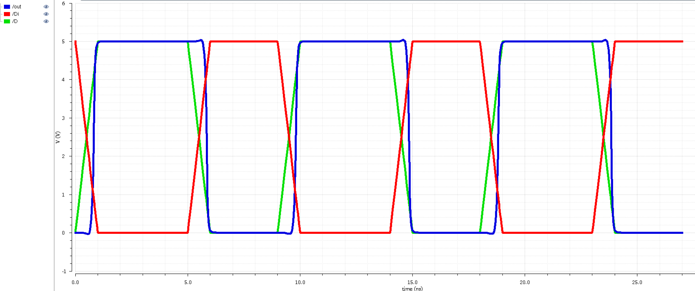
The receiver can also handle
a little over a 2 ns bit-width; however, the performance is affected
negatively as seen in the output low.
Flaws:
At plain sight, we can see that my output could be sharper and
more decisive. The phase could definitely be improved. The performance
also suffers when it's inputs are away from VDD/2. There are probably
more, but those are the ones I'd like to point out.
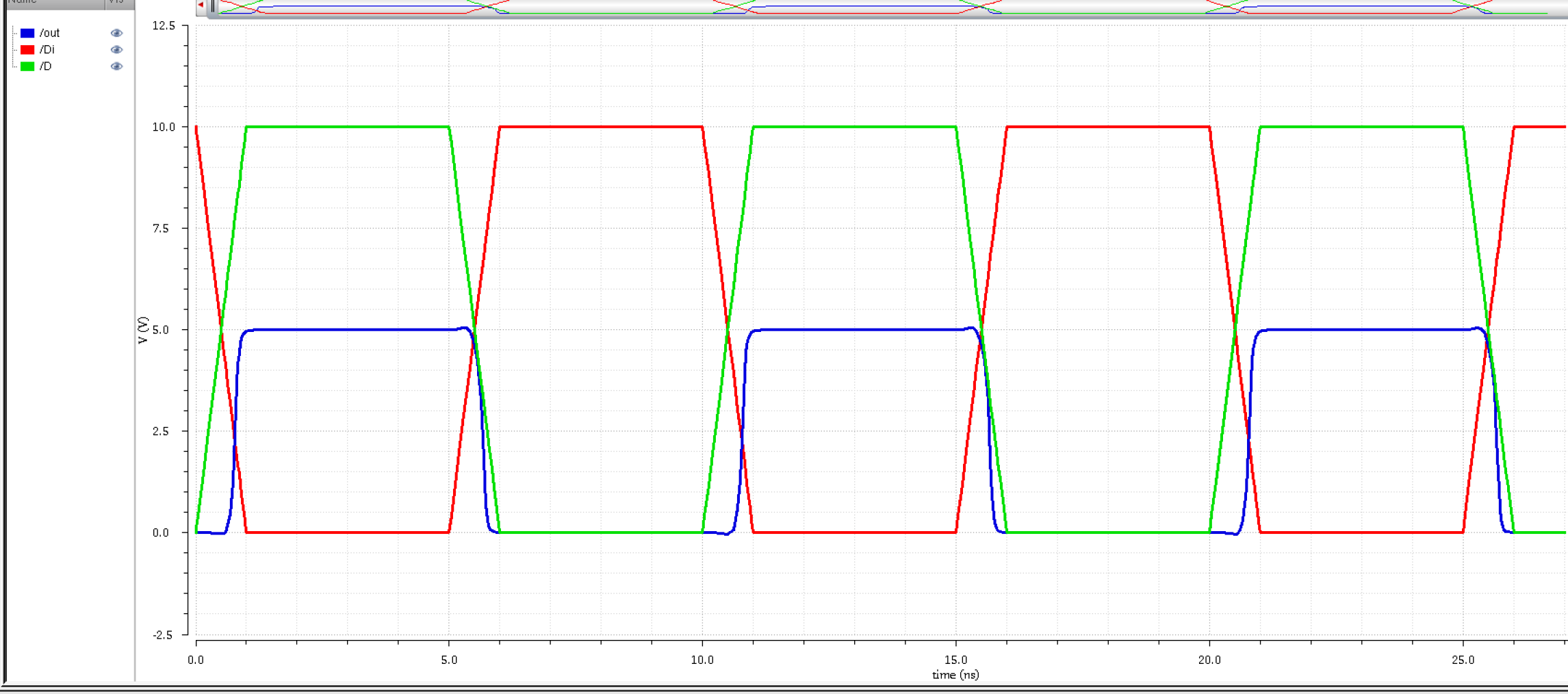
Inputs: 1V and 0.75V
|
Inputs: 5V and 4.75
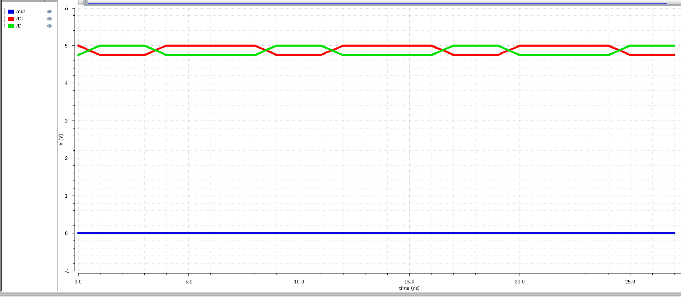
|
The bit-width got bigger at 1V and 0.75V. At 5V and 4.75V, we flat out don't get an output.
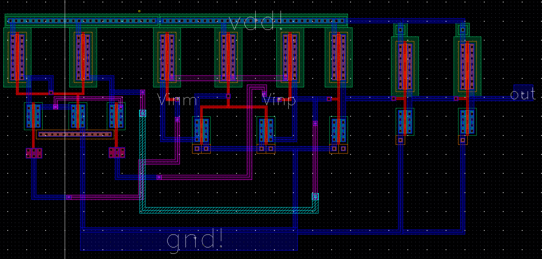
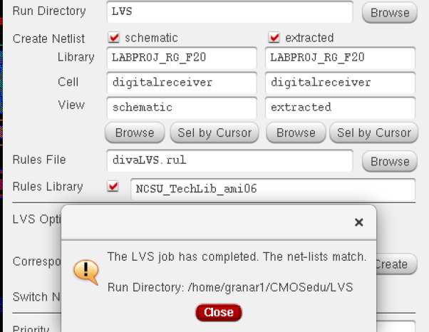
Layout, DRC, LVS :

File-Backup Proof:
Conclusion
This project was quite
challenging and rewarding at the same time. It required me to really
delve into the book and focus so deeply on one particular aspect of it:
input buffers. Even though my design wasn't as good as I hoped, I have
learned a lot about a device that is used in the real world. I am
ecstatic to have one more thing to talk to would-be interviewers about.
Though things have been hectic around me, and I have been personally
affected by the pandemic, I take pride in perserving through this
project and completing it as best as I could. There's a million things
I wish I could have done. You'll notice that I don't have as many
calculations as my peers, that is due to me running out of time, and
not wanting to make Dr. Baker wait too long to grade my work. It
wouldn't be fair for the others if I got an extension, we're all going
through a pandemic and have our own problems; however, I am sure we
will all get through it! With that, I'm glad I got to work on this
project before I graduated!
Return to EE421L Labs by granar1