Lab 7 - EE421L
Authored
by Rhyan Granados
Email: granar1@unlv.nevada.edu
10/23/20
Goal
Using buses and arrays in the design of word inverters, muxes, and high-speed adders
Prelab
I backed up my work for Lab 6
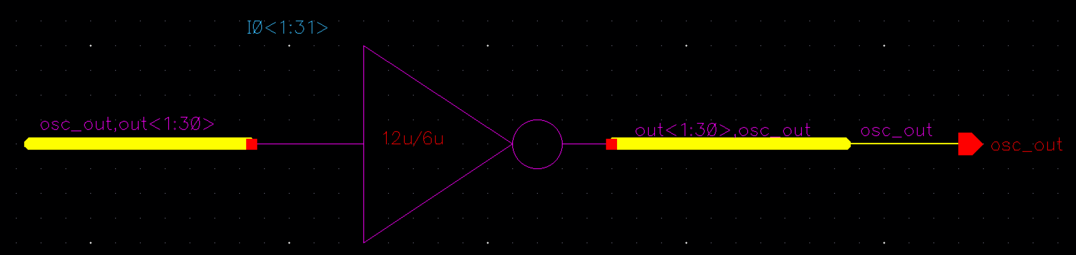
I completed Tutorial 5 as seen below
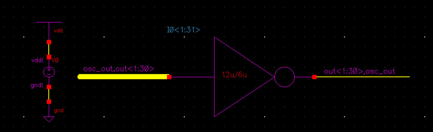
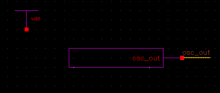
Schematic:

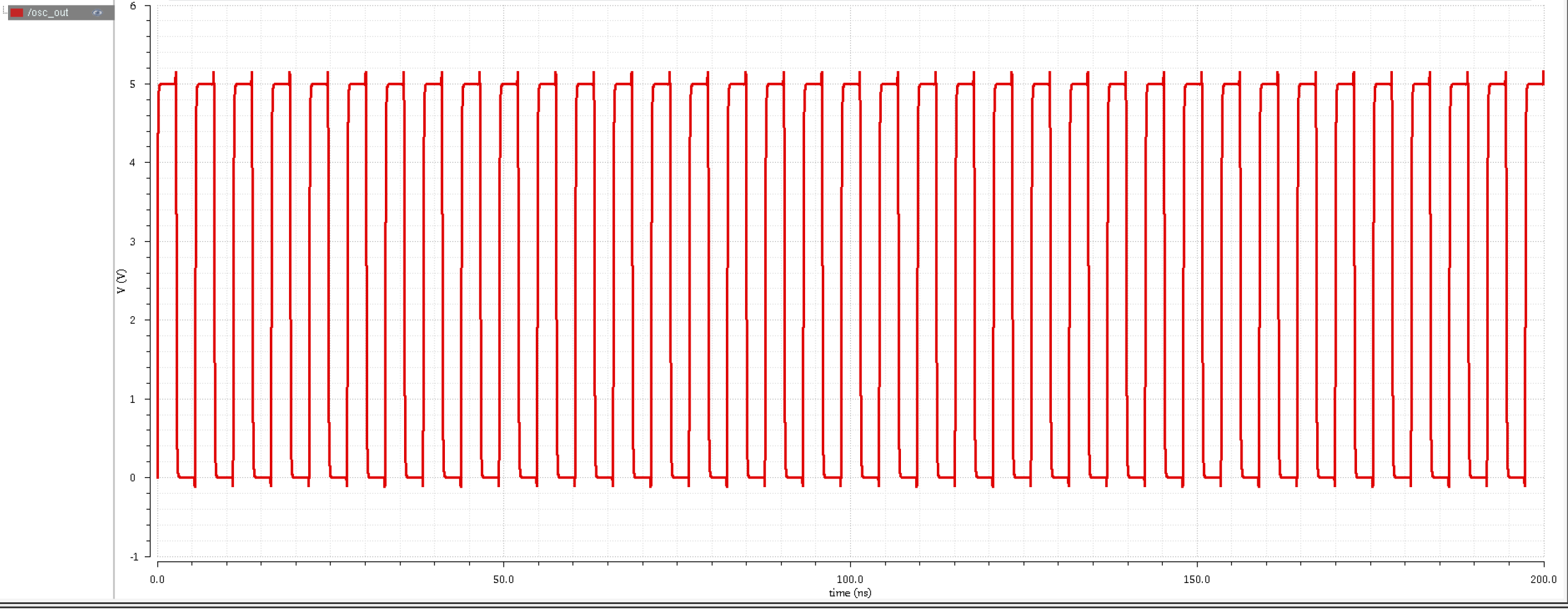
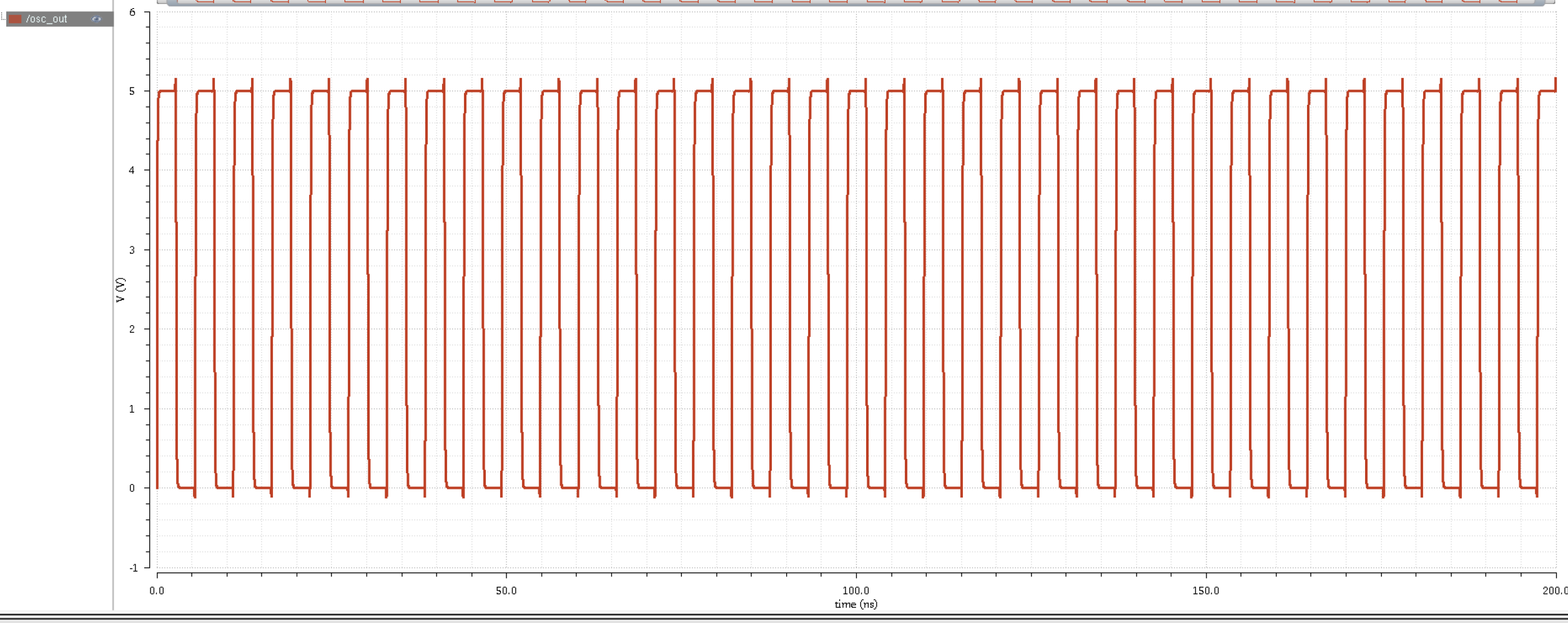
Sim:
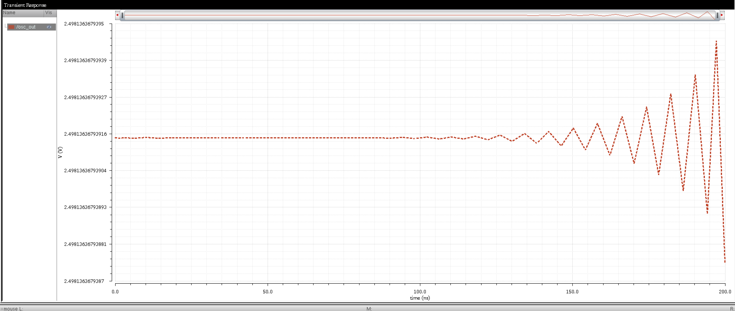
Sim with init. condition of osc_out at 0V:
Alternative More Concise Schematic:
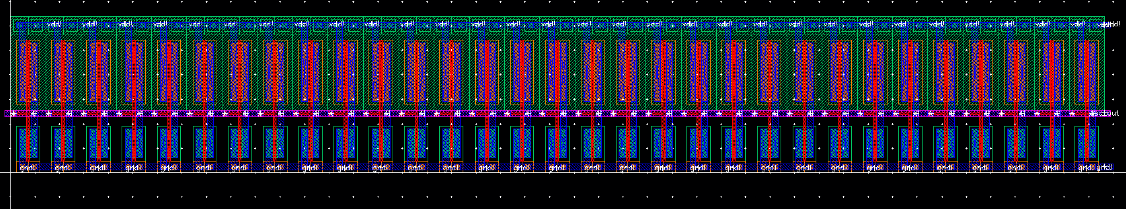
Final Layout:
Schematic for Layout:
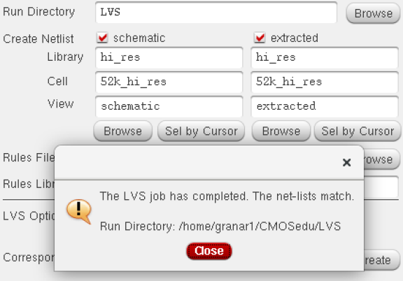
LVS:
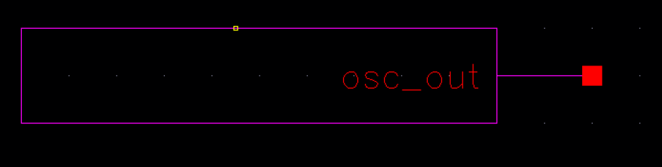
Symbol:
Sim Schematid:
|
Sim Results:
|
The Lab
1) Simulate the 4-bit inverter circuit
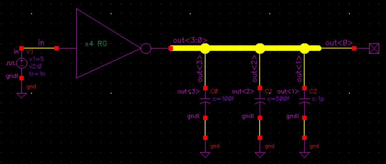
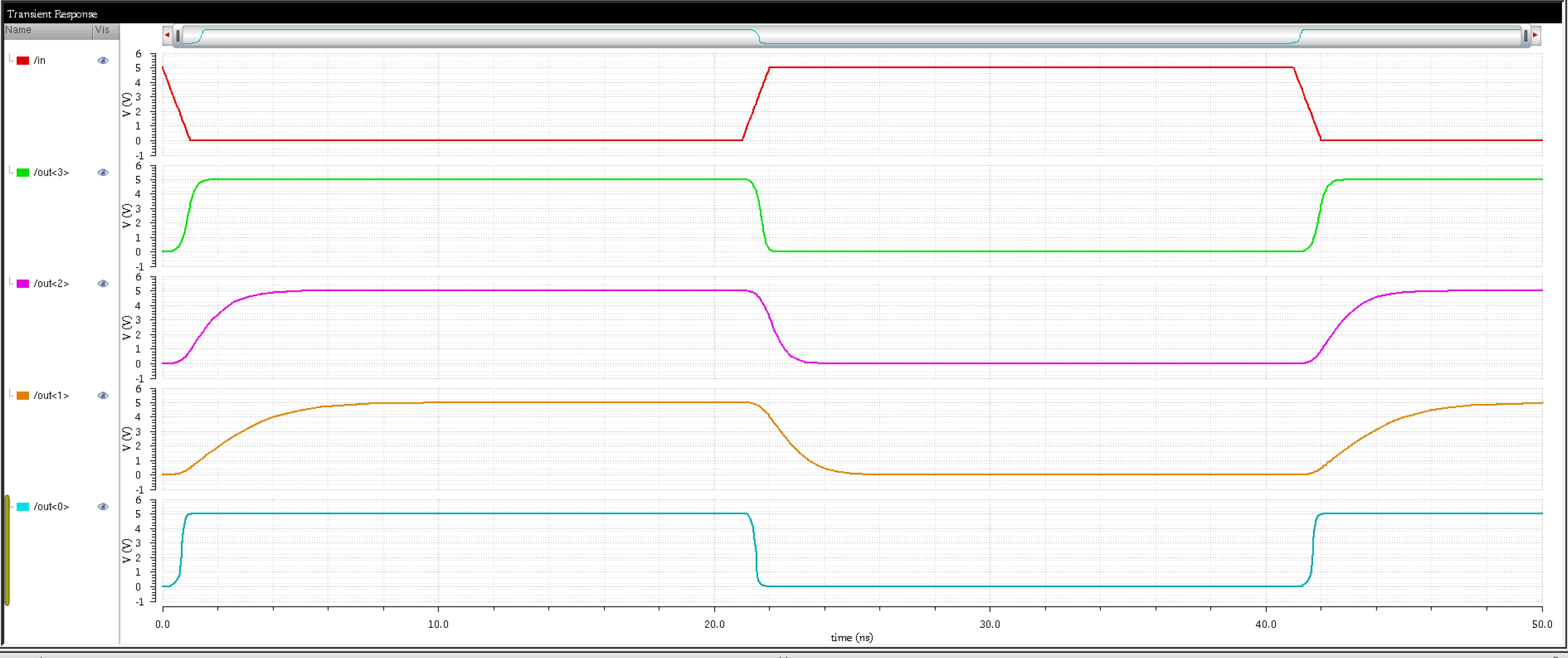
As you can see from the
graph, since out<1> has the largest load attached to it, it will
have the longest rise time. While, out<0>takes the least amount
of time to rise due to having no load.
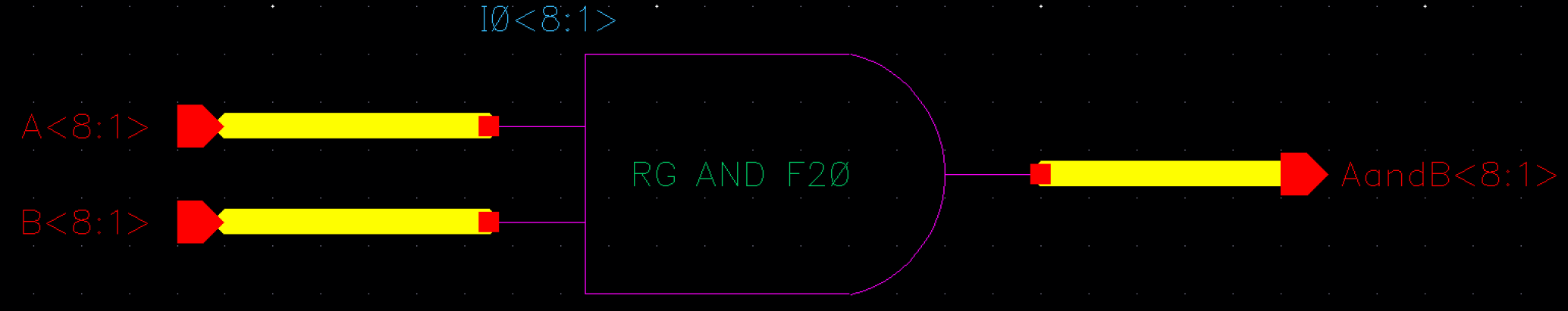
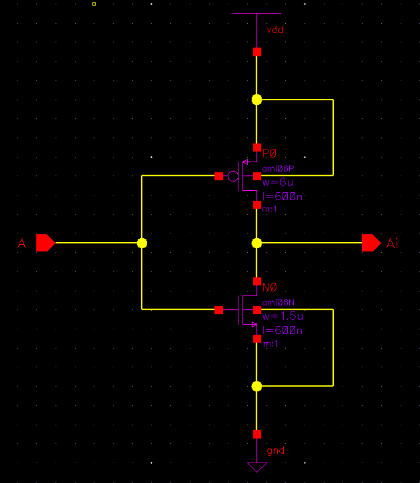
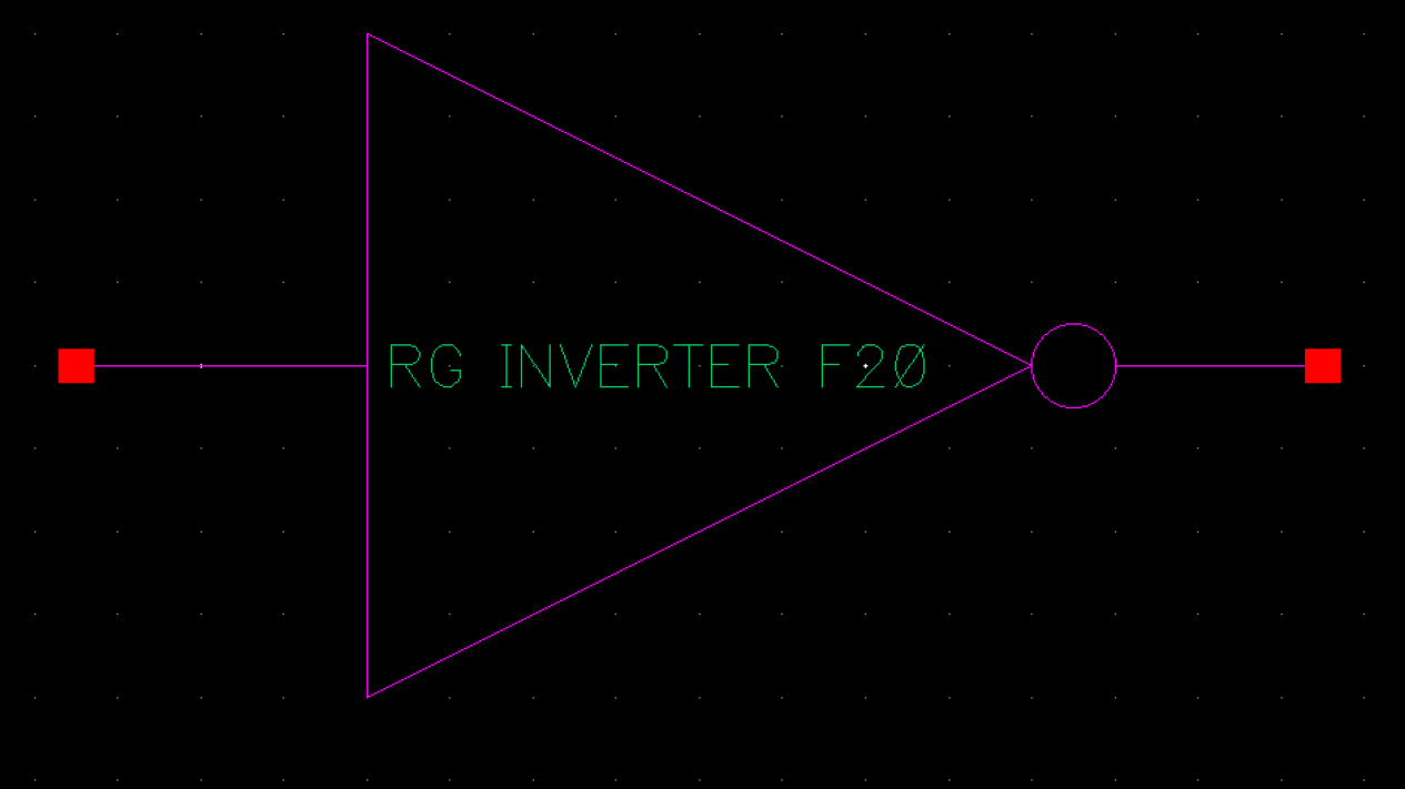
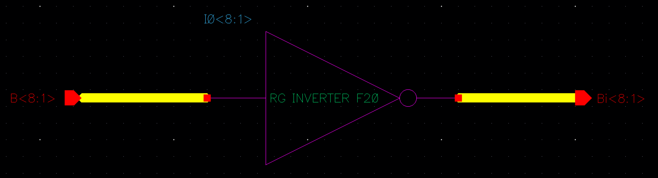
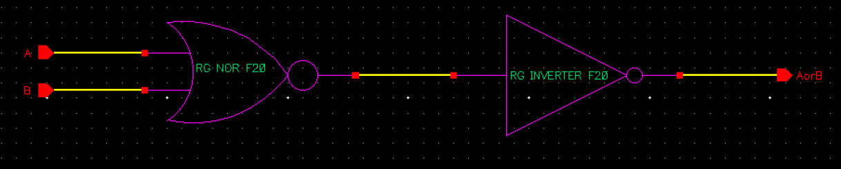
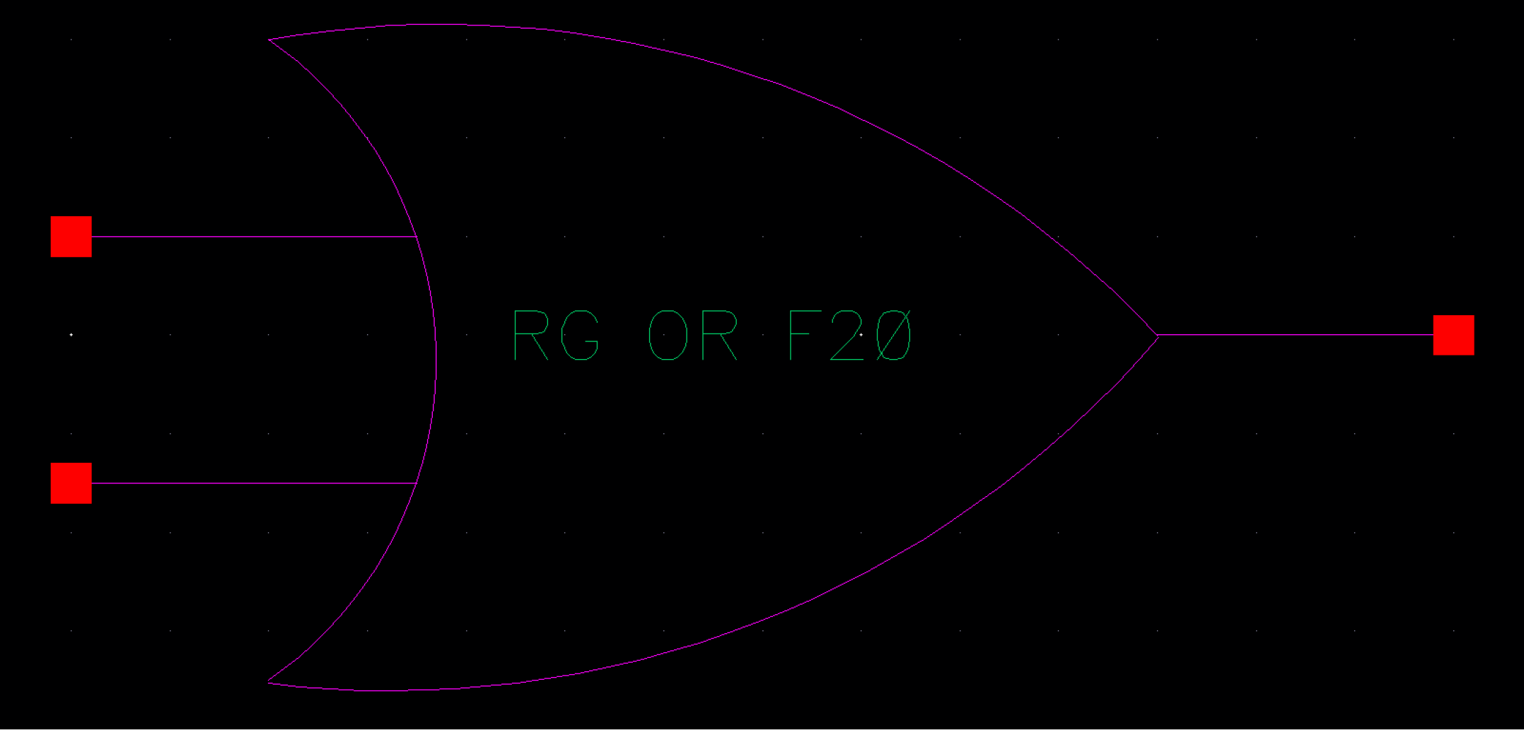
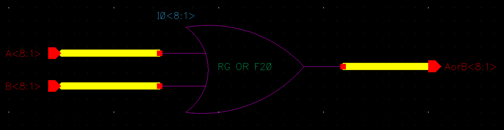
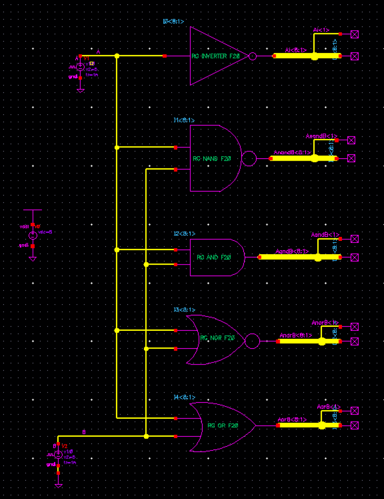
2) Create schematics and symbols for an 8-bit input/output array of: NAND, NOR, AND, inverter, and OR gates.
Provide a few simulation examples using these gates.
|
Schematic
|
Symbol
|
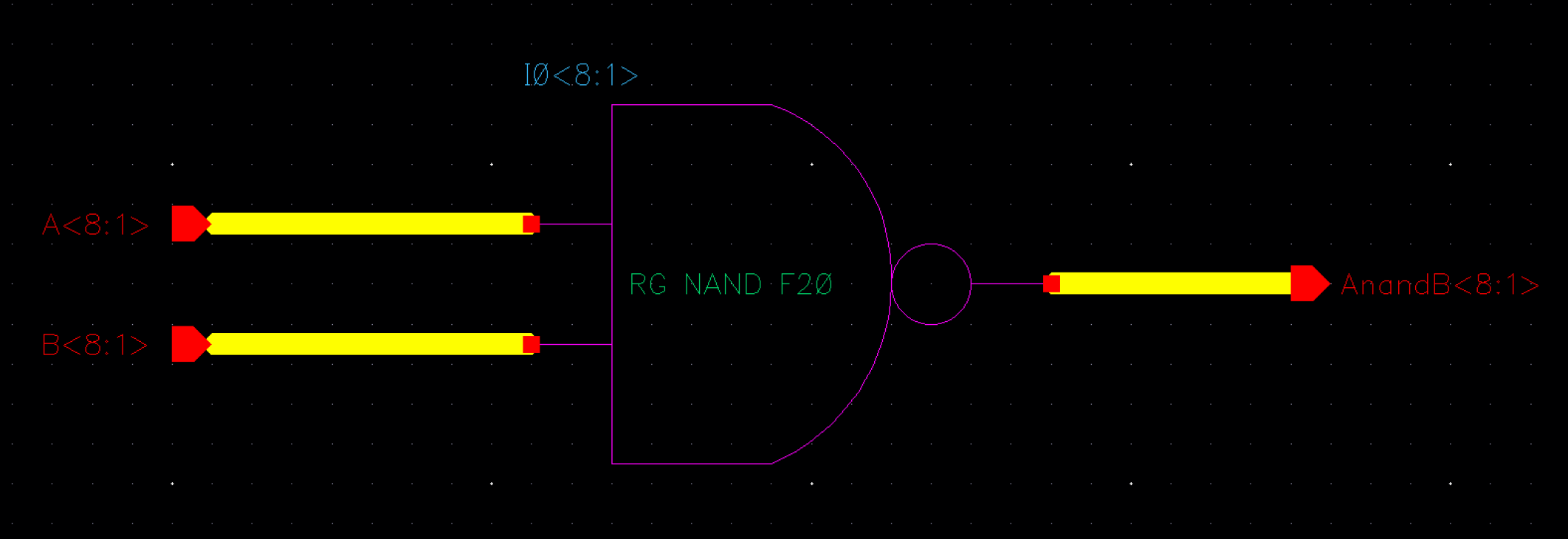
8-Bit Schematic
|
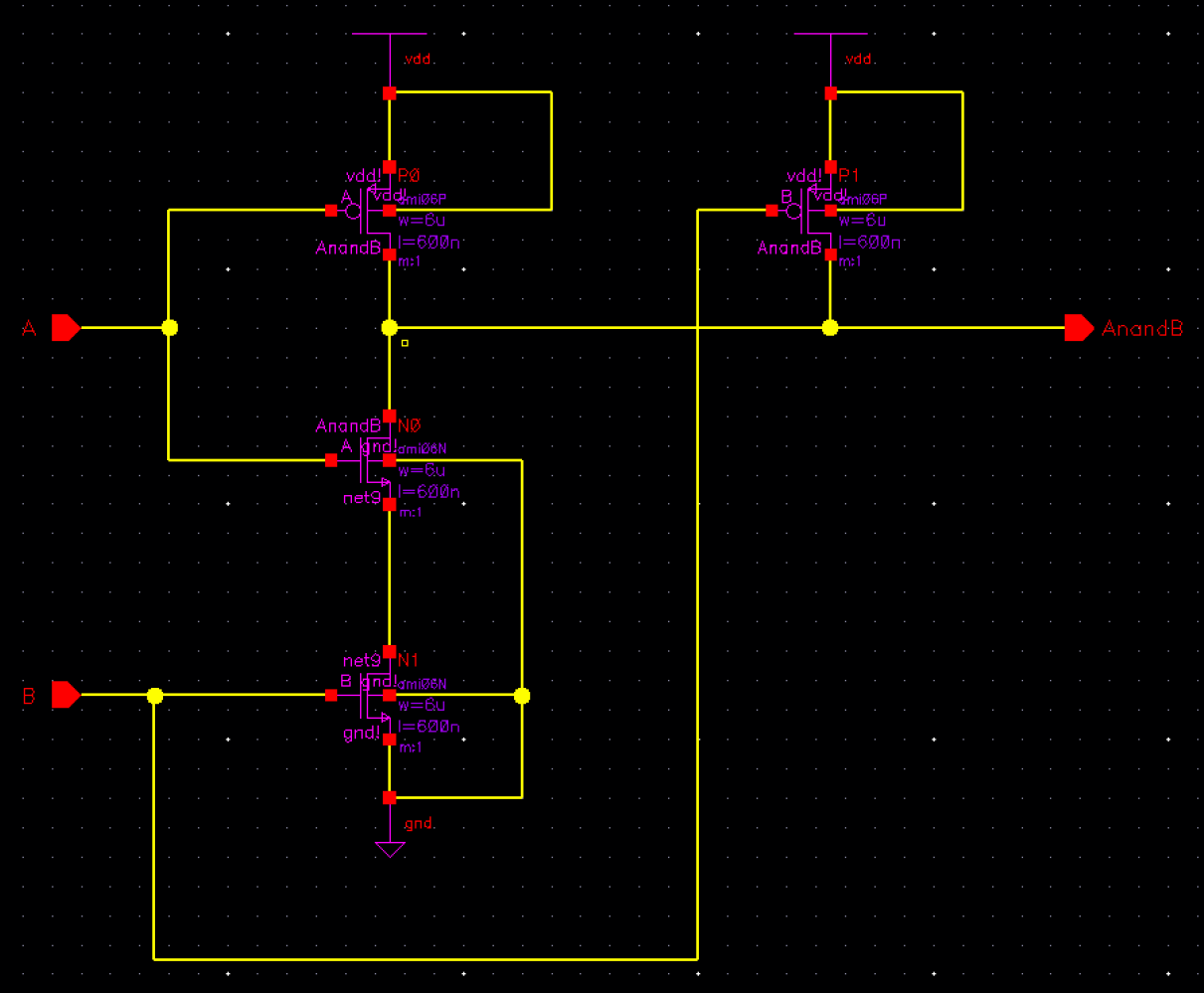
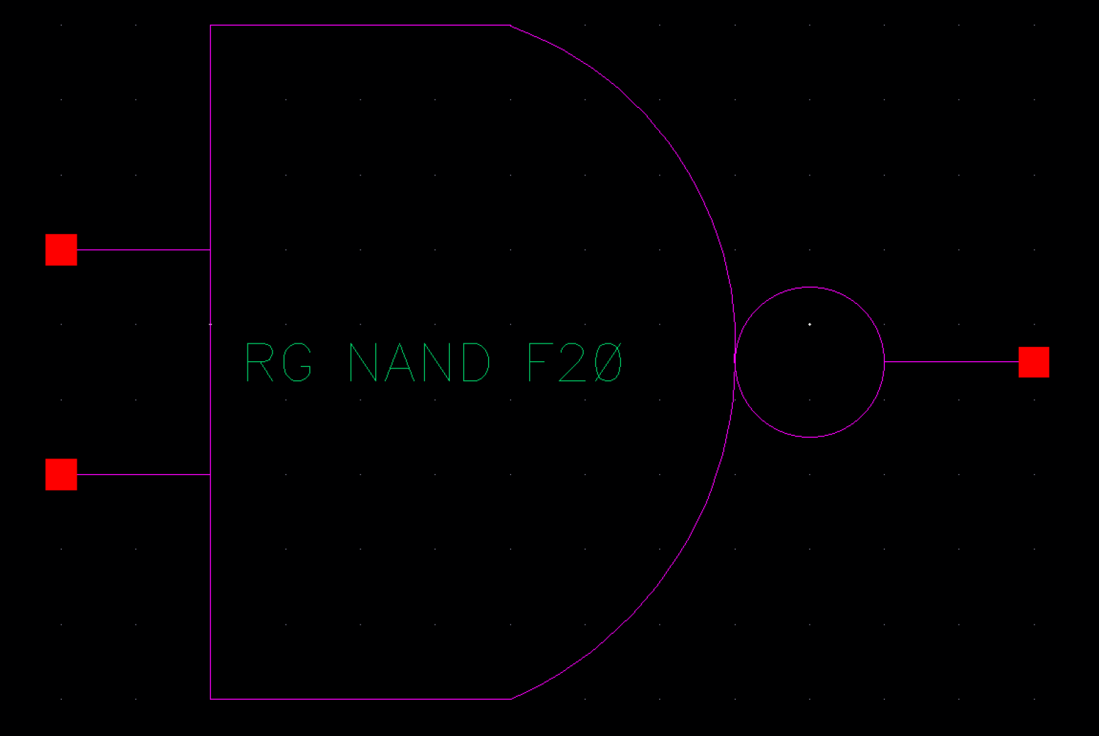
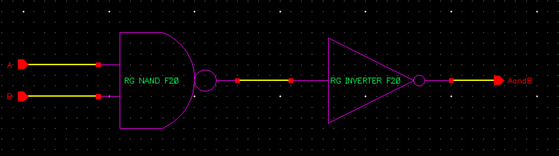
| NAND |
|
|
|
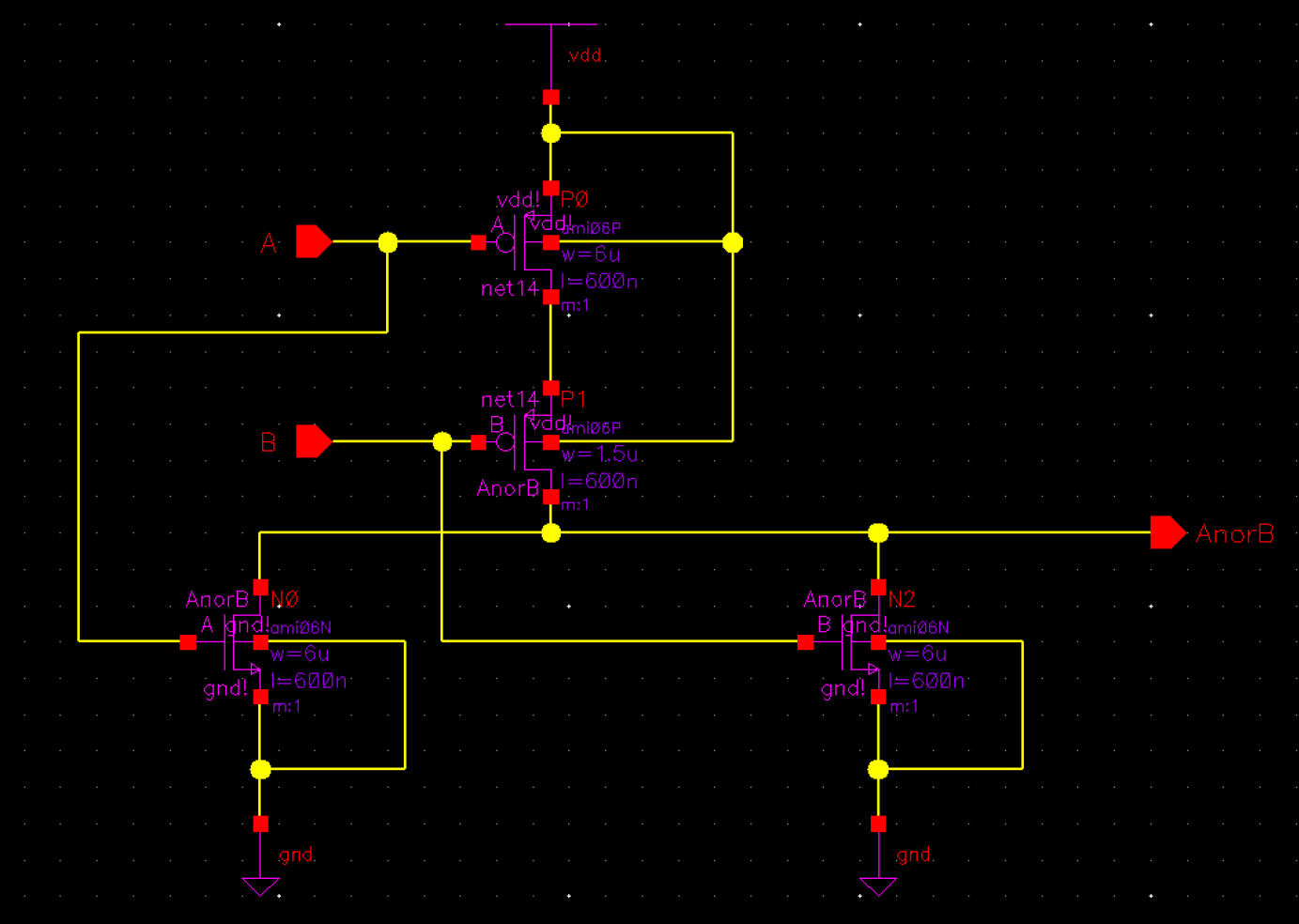
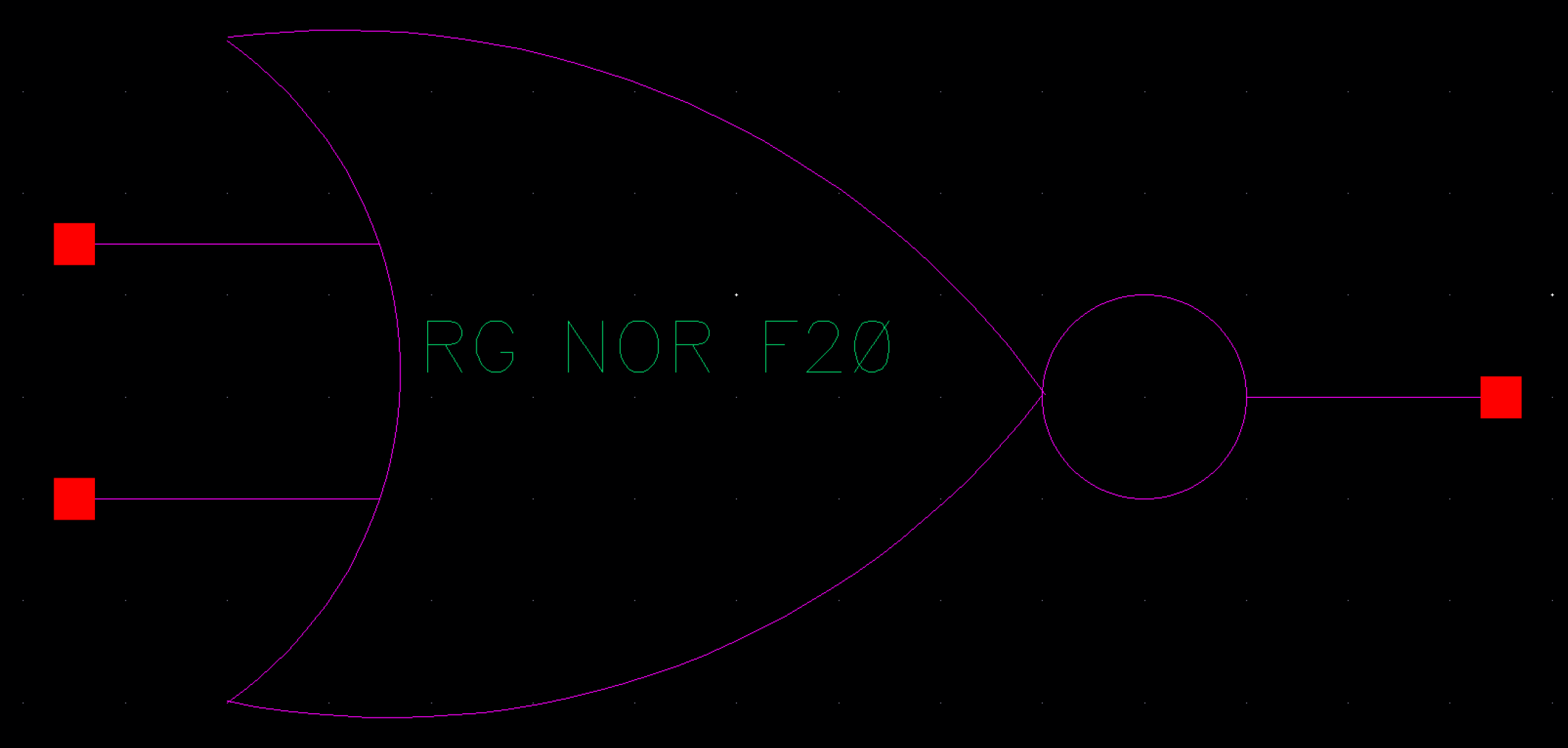
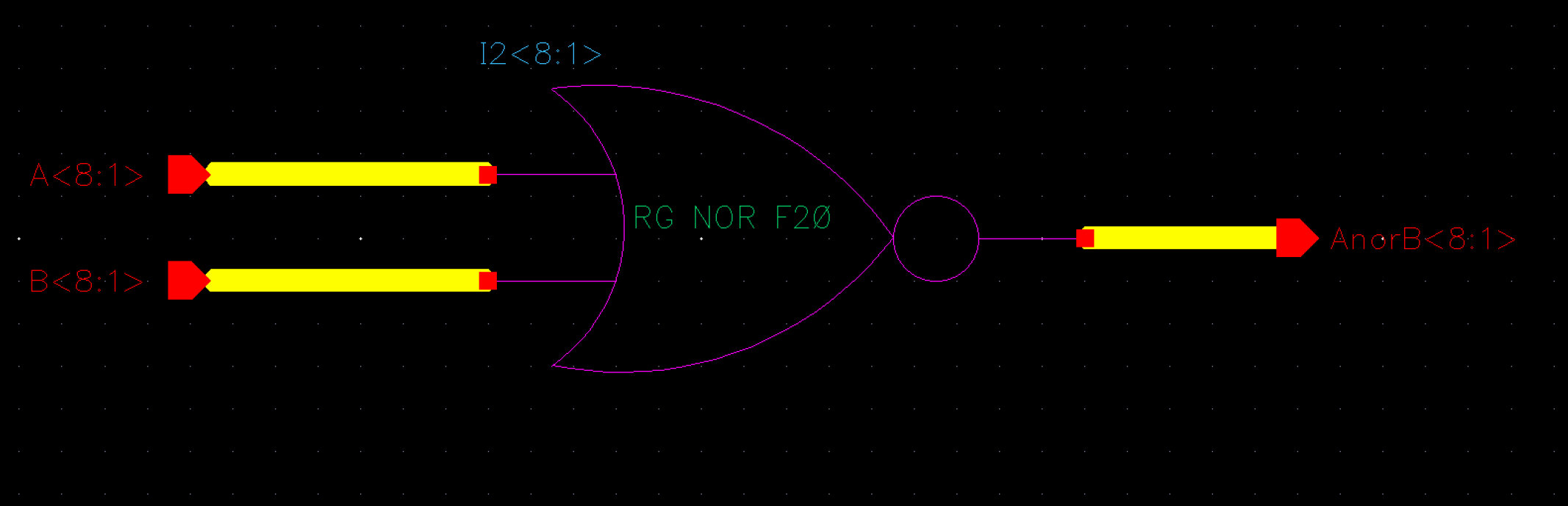
NOR
|
|
|
|
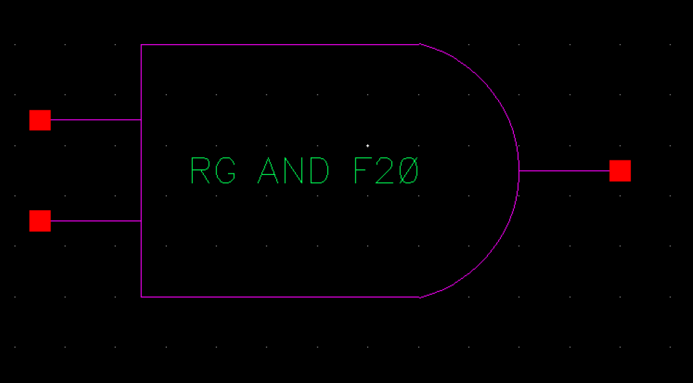
| AND |
|
|
|
| inverter |
|
|
|
OR
|
|
|
|
Simulation of all 2-input gates:
3)
Next examine the following schematic of a 2-to-1 DEMUX/MUX (and the
symbol). Simulate the operation of this circuit using Spectre and
explain how it works.
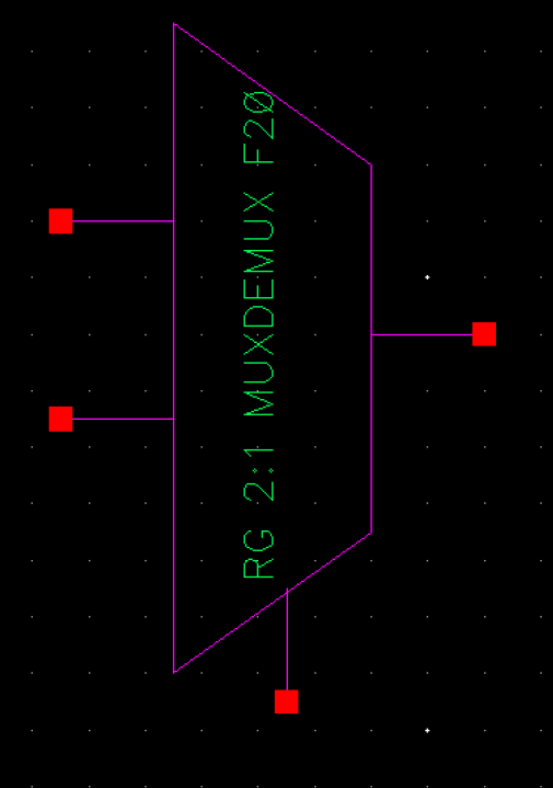
1-Bit Mux/Demux
Schematic
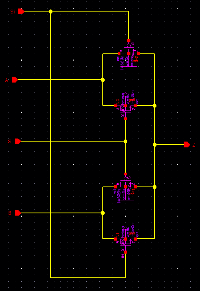
|
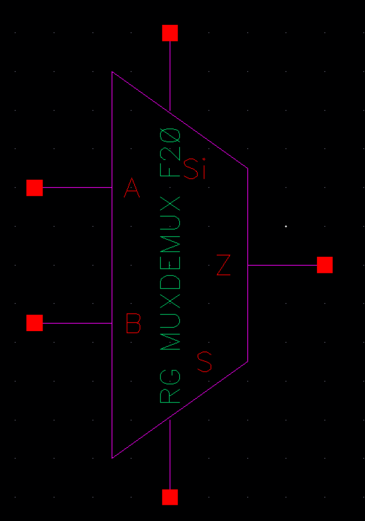
|
1-Bit 2:1 Demux/Mux
Schematic
|
|
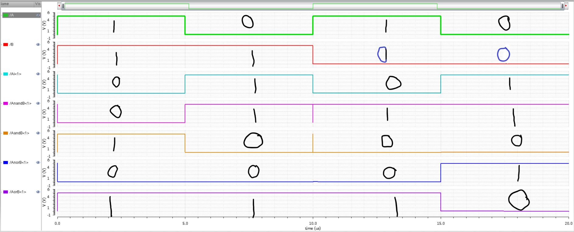
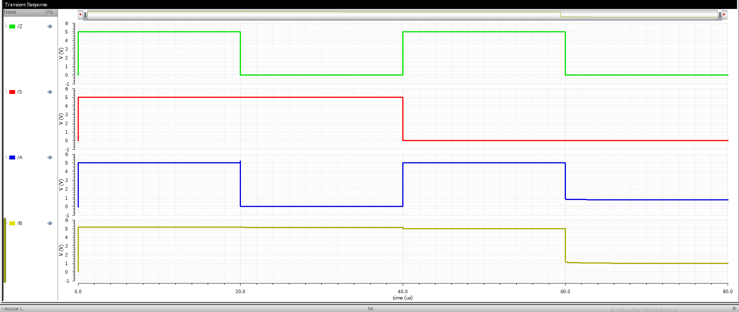
1-Bit 2:1 Mux Sim
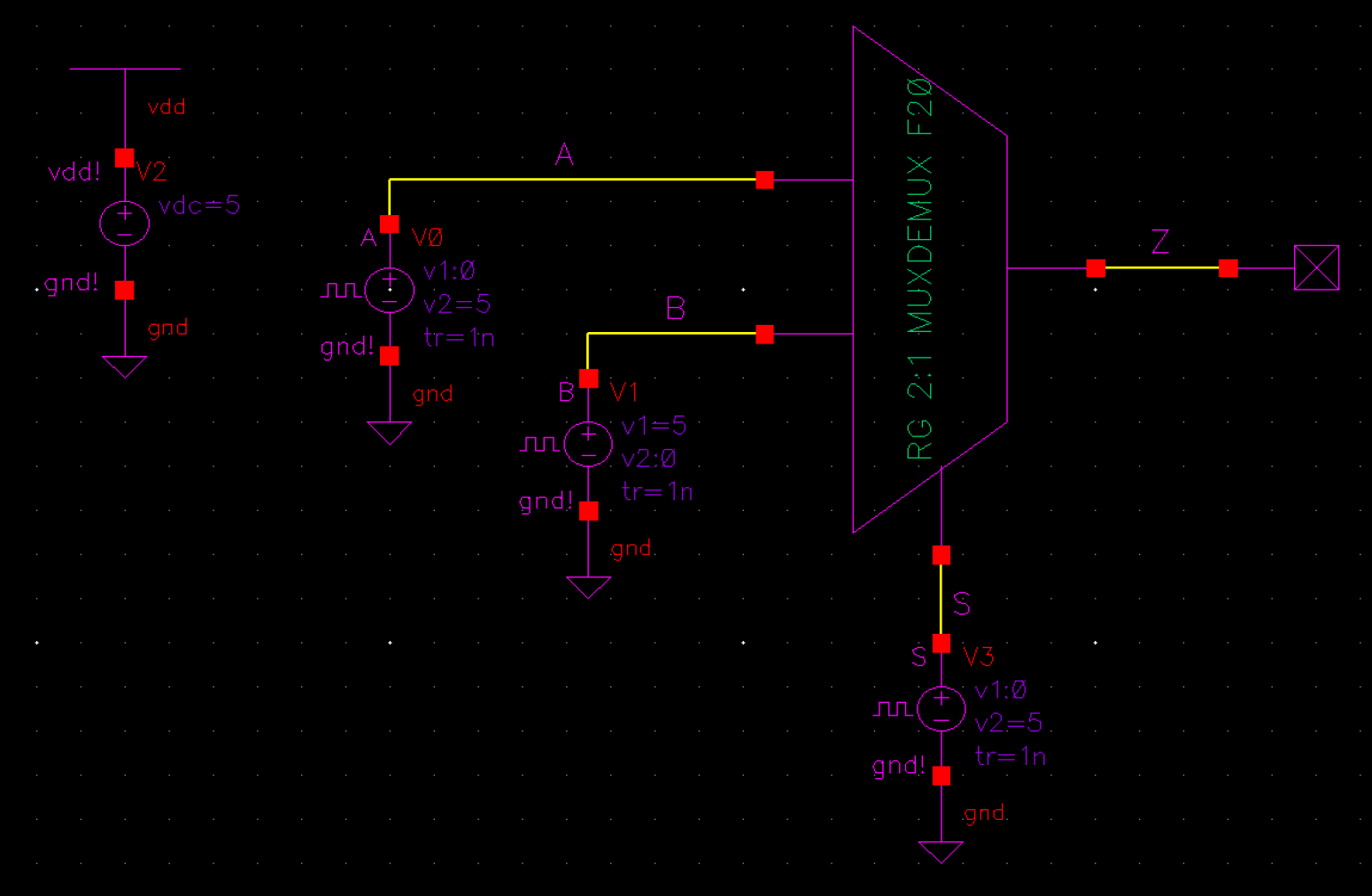
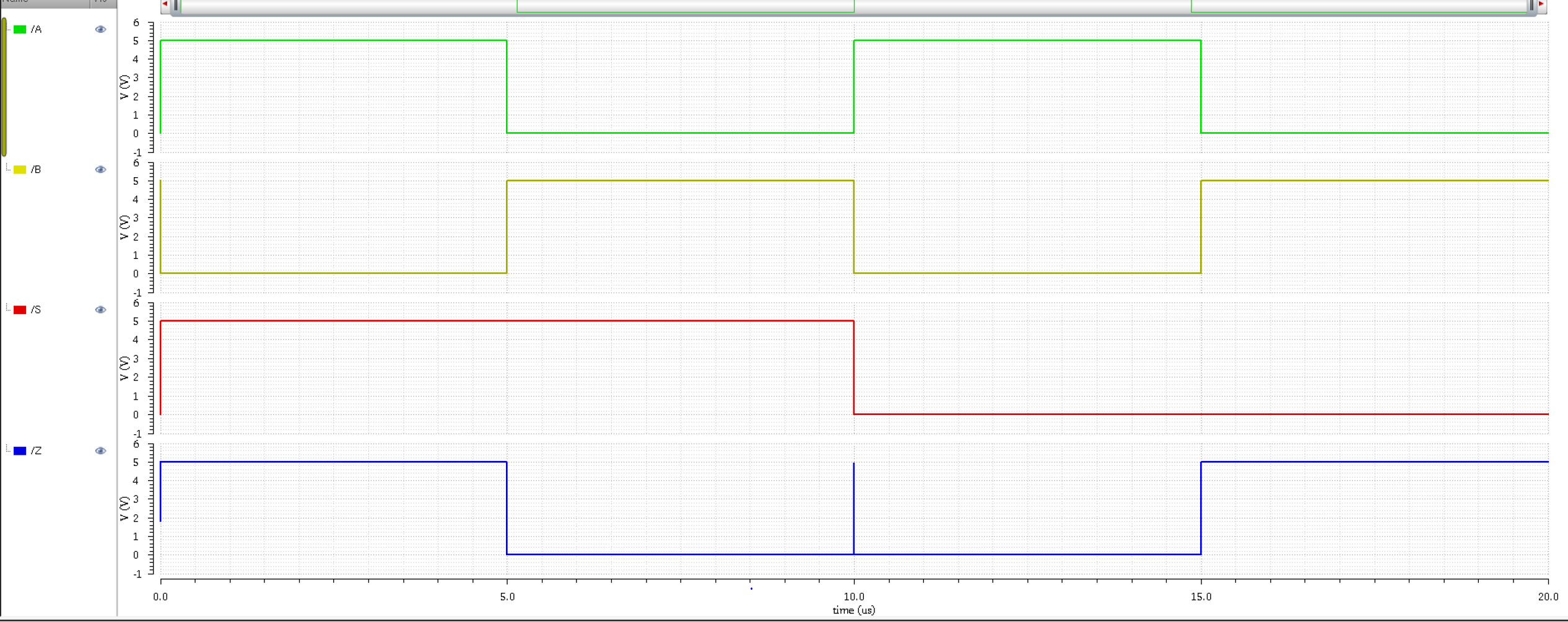
As we can see on the
simulation, the multiplexer works by using S to choose the output
signal Z. So if S is high then it will pass A's signal as the output Z,
and if S is low(Si becomes high due to the inversion) and B's signal is
passed through as the output Z.
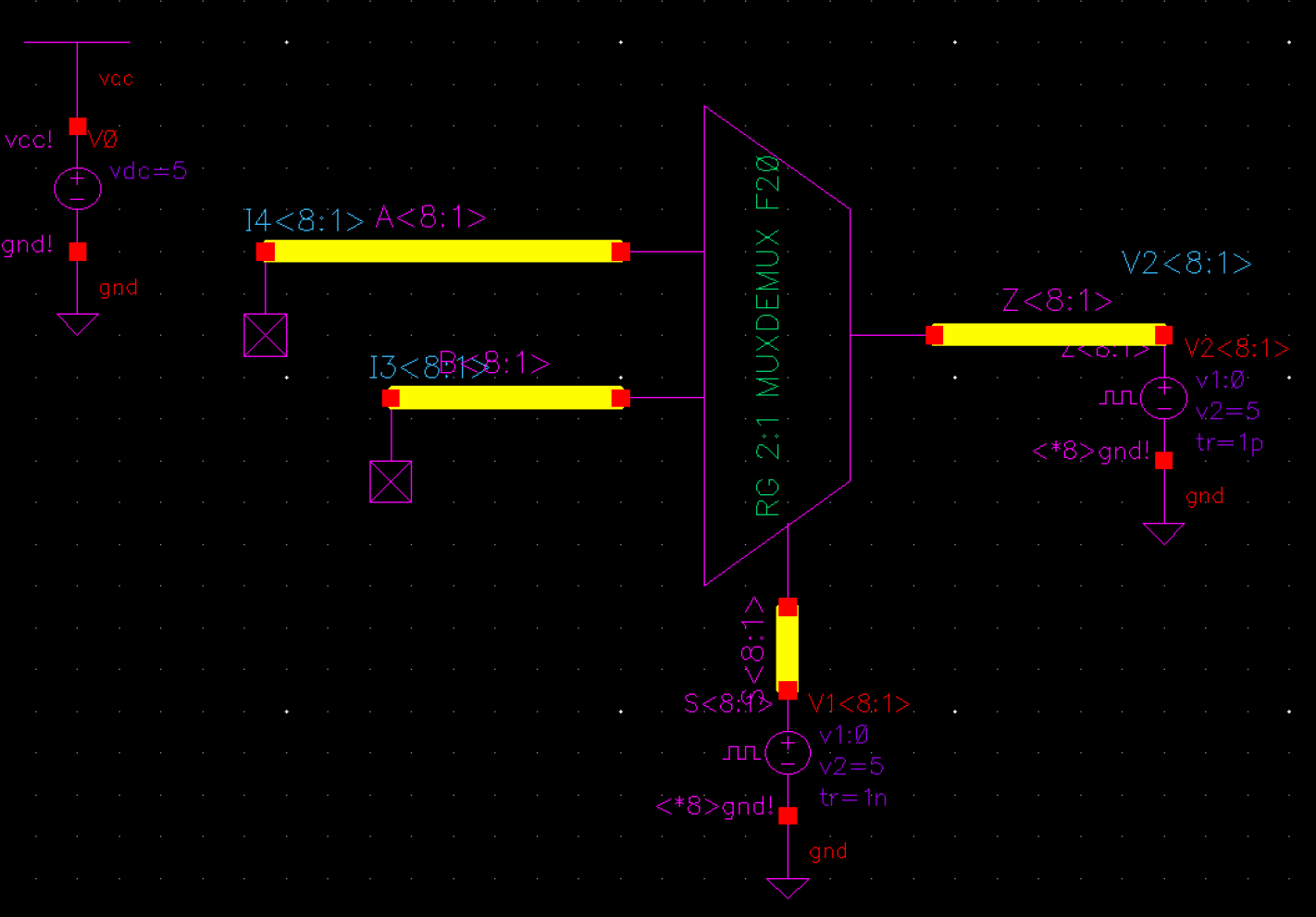
1-Bit 2:1 Demux Sim
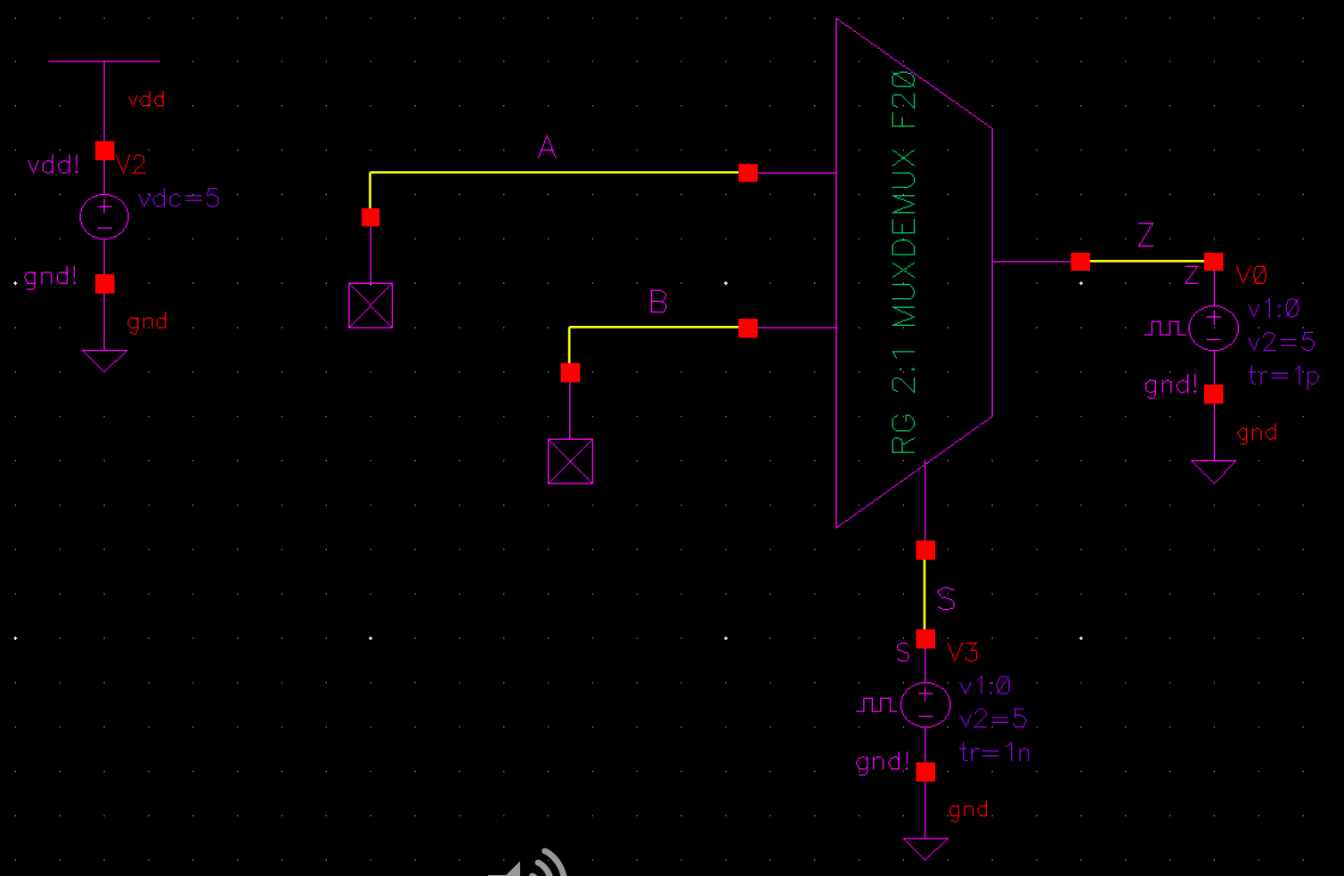
As we can see from the sims
the demultiplexer does the opposite of the multiplexer. Instead of
using S to choose which signal to pass through as the output Z, it
takes Z as the input and uses S to decide where Z will go. So if S is
high then Z goes to A and inversely goes to B when it's low.
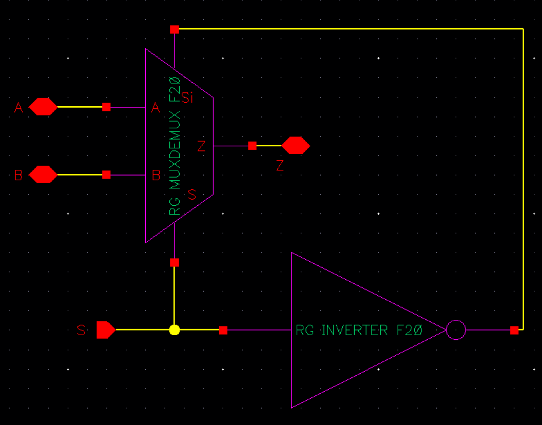
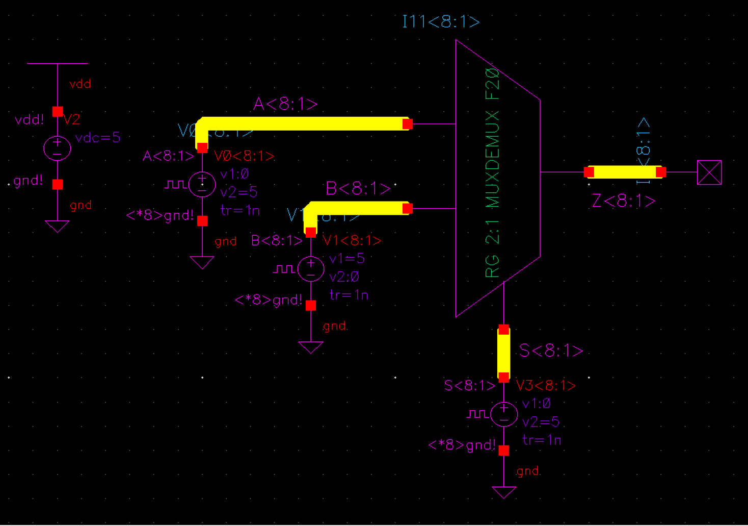
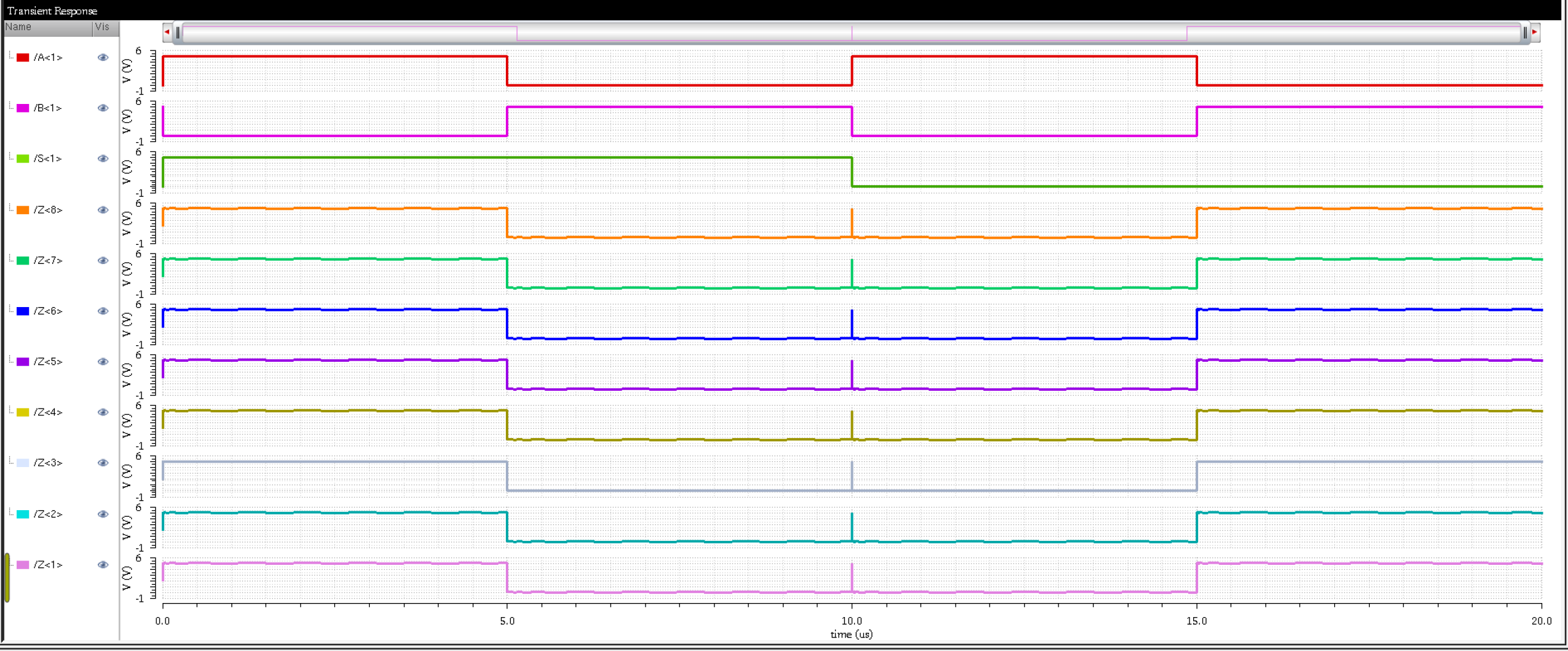
4) Create an 8-bit wide word 2-to-1 DEMUX/MUX schematic and symbol.Include
an inverter in your design so the cell only needs one select input, S
(the complement, Si, is generated using an inverter).Use simulations to verify the operation of your design.
Note: So I already included the inverter in part 3) so I will just re-use it
8-Bit 2:1 Mux Sim
8-Bit 2:1 Demux Sim
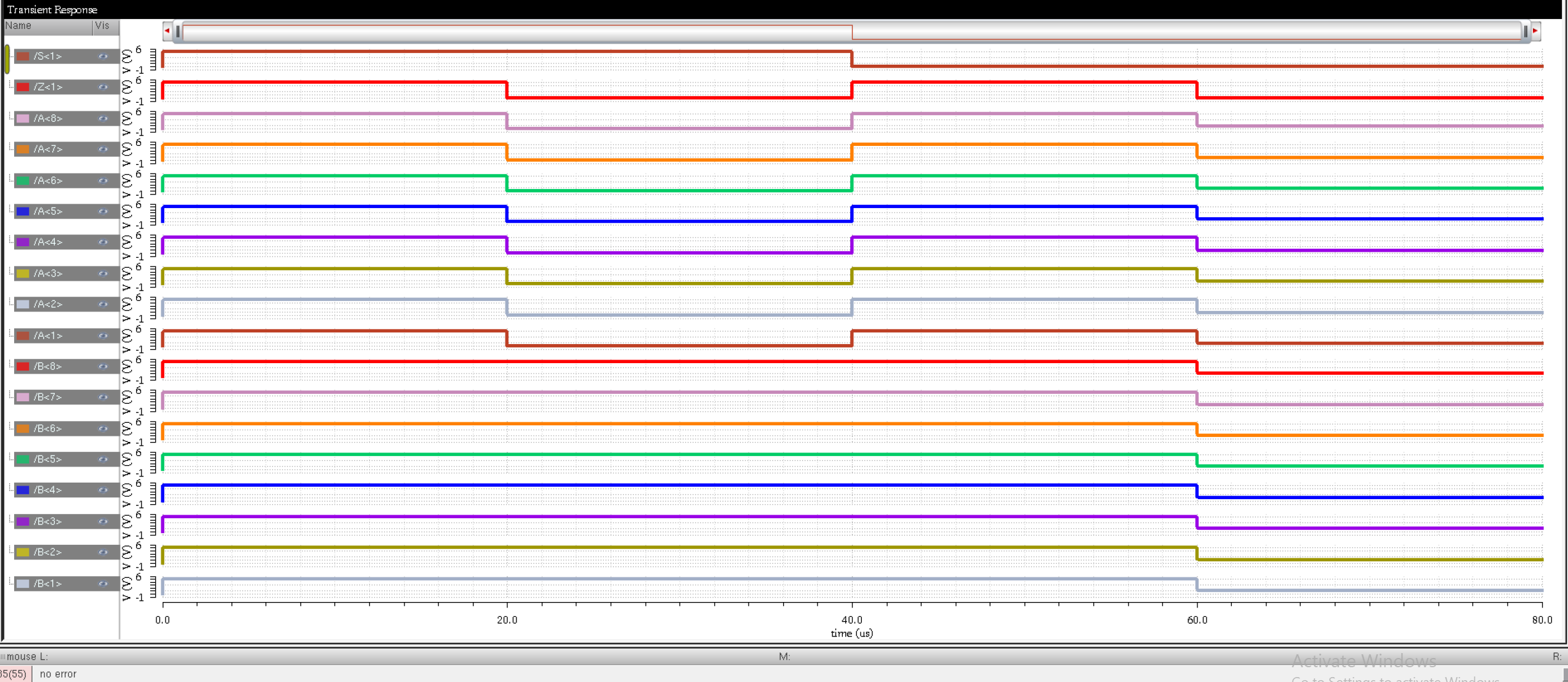
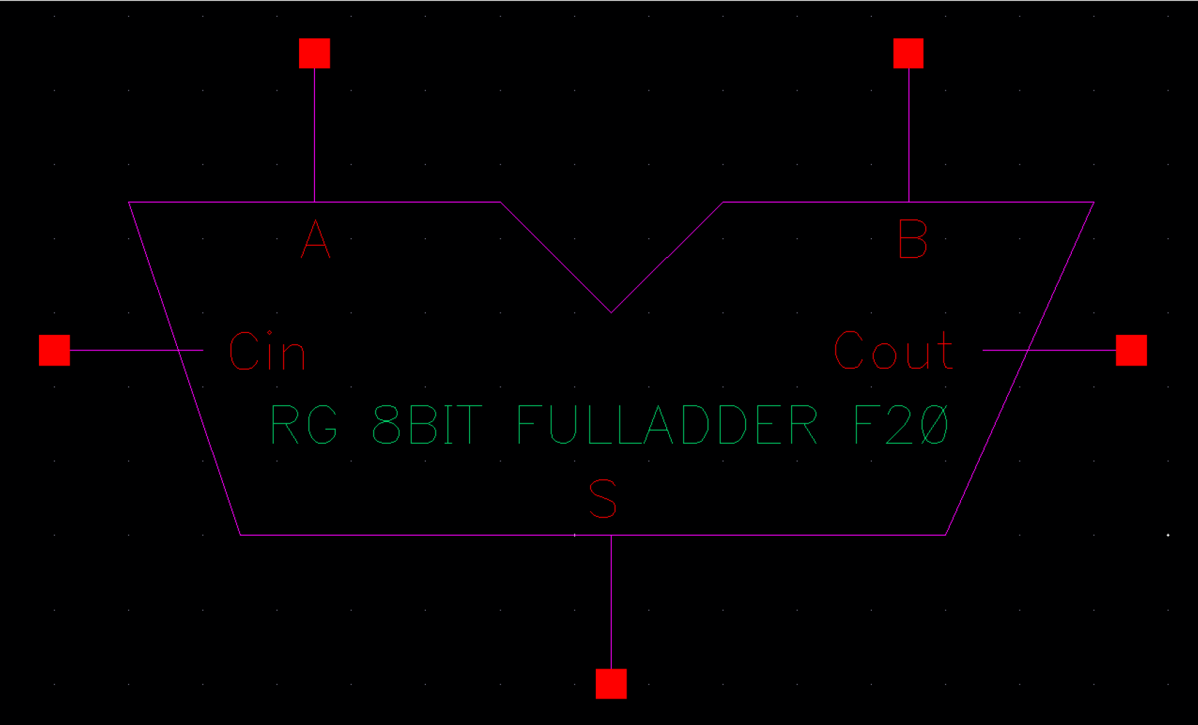
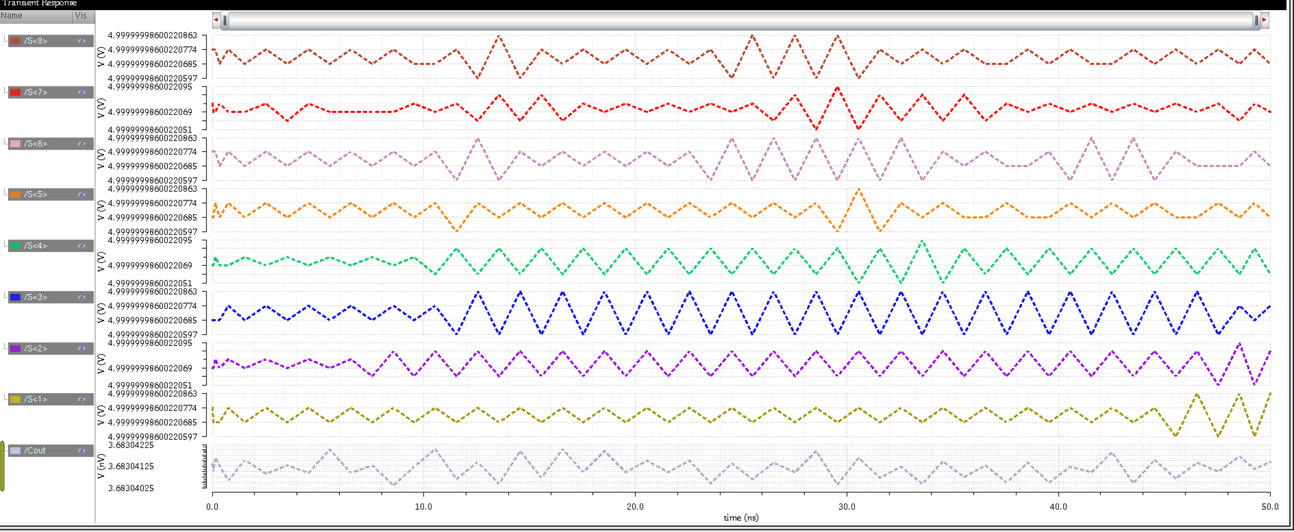
5) Simulate the operation of your 8-bit adder.
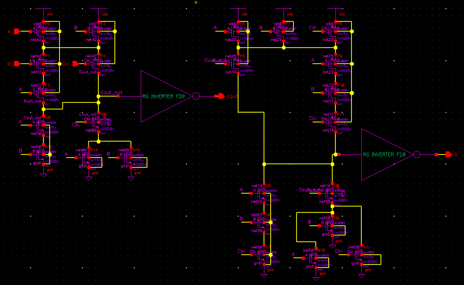
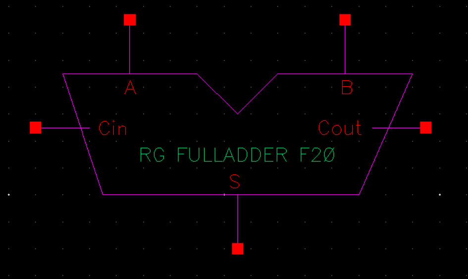
1-Bit Full Adder
Schematic
|
|
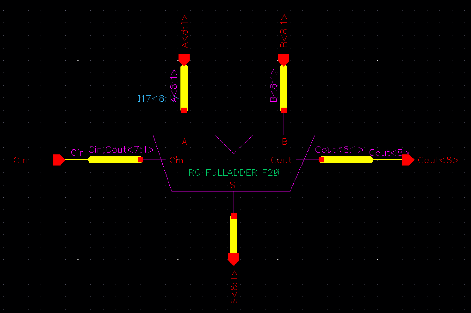
8-Bit Full Adder
Schematic
|
|
Simulation
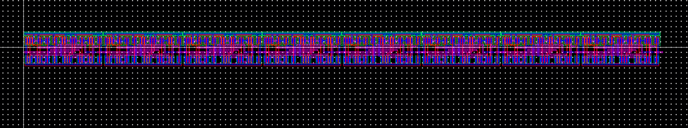
Lay out this 8-bit adder cell (*note* that this is the only layout required in this lab).
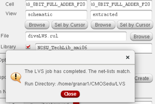
Show that your layout DRCs and LVSs correctly.
Layout
DRC and LVS Certification:

File Back-up Proof
Return to EE421L Labs by granar1