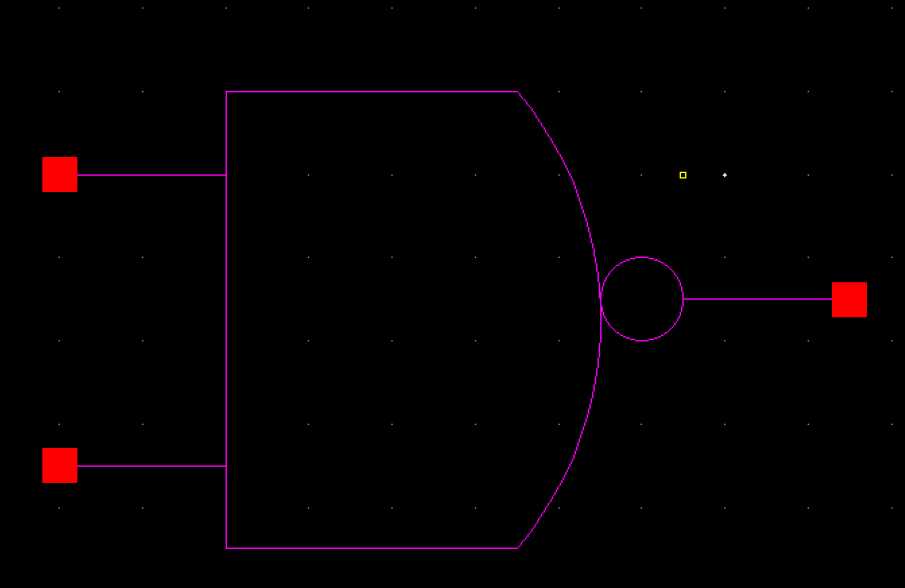
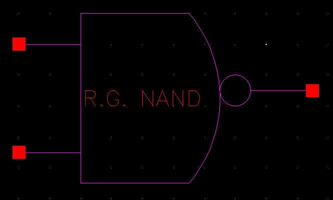
 Nand Symbol
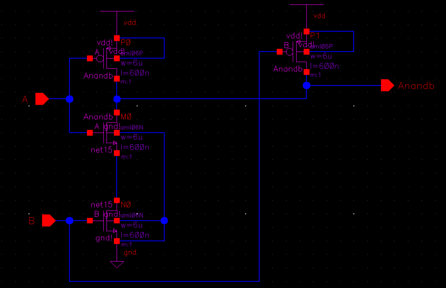
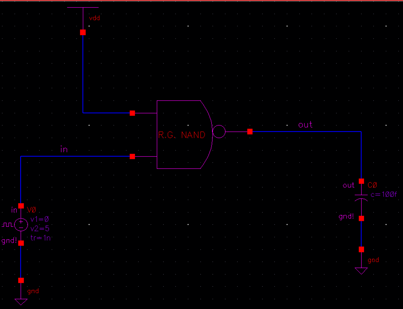
Nand Schem
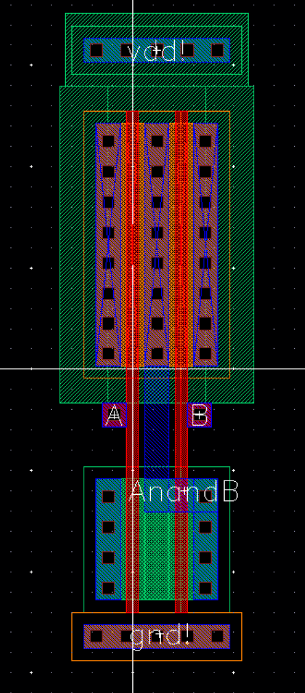
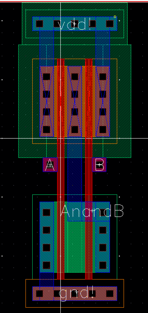
Nand Layout
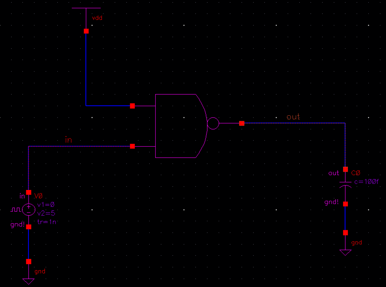
Nand in a Circuit
Lab 6 - EE421L
Design, layout, and simulation of a CMOS NAND gate, XOR gate, and Full–Adder
| Nand Symbol |
Nand Schem |
Nand Layout |
Nand in a Circuit |
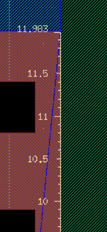
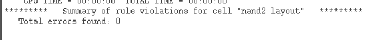 DRC Certification |
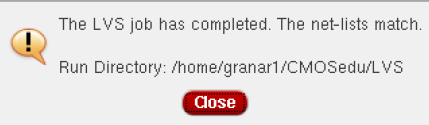
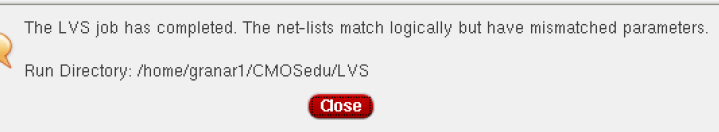 LVS Certification |
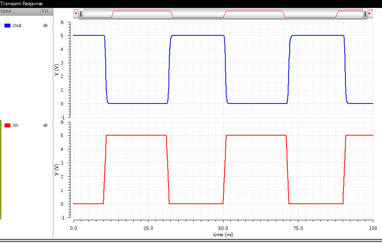 Simulation Results |
The Lab
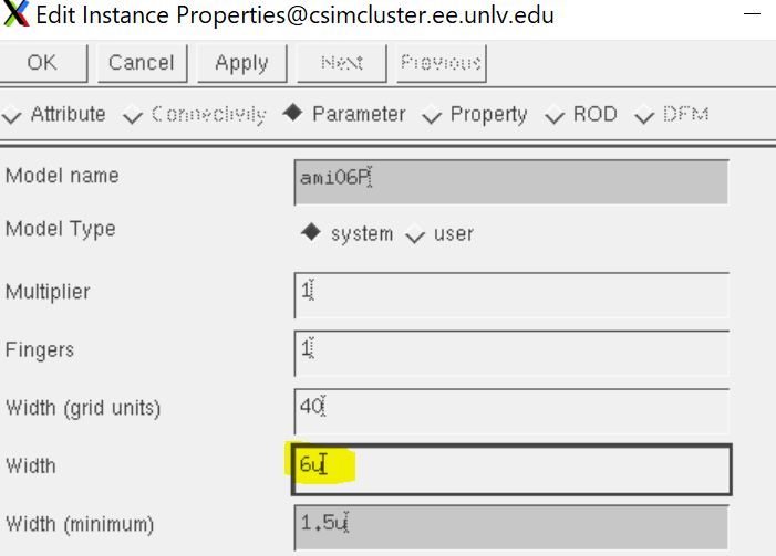
1) Draft the schematics of a 2-input NAND gate (Fig. 12.1), and a 2-input XOR gate (Fig. 12.18) using 6u/0.6u MOSFETs (both NMOS and PMOS)
 2-input Nand Symbol |
2-input Nand Schem |
 2-input Nand Layout |
 2-input Nand in a Circuit |
 |
 |
 DRC Certification |
 LVS Certification |
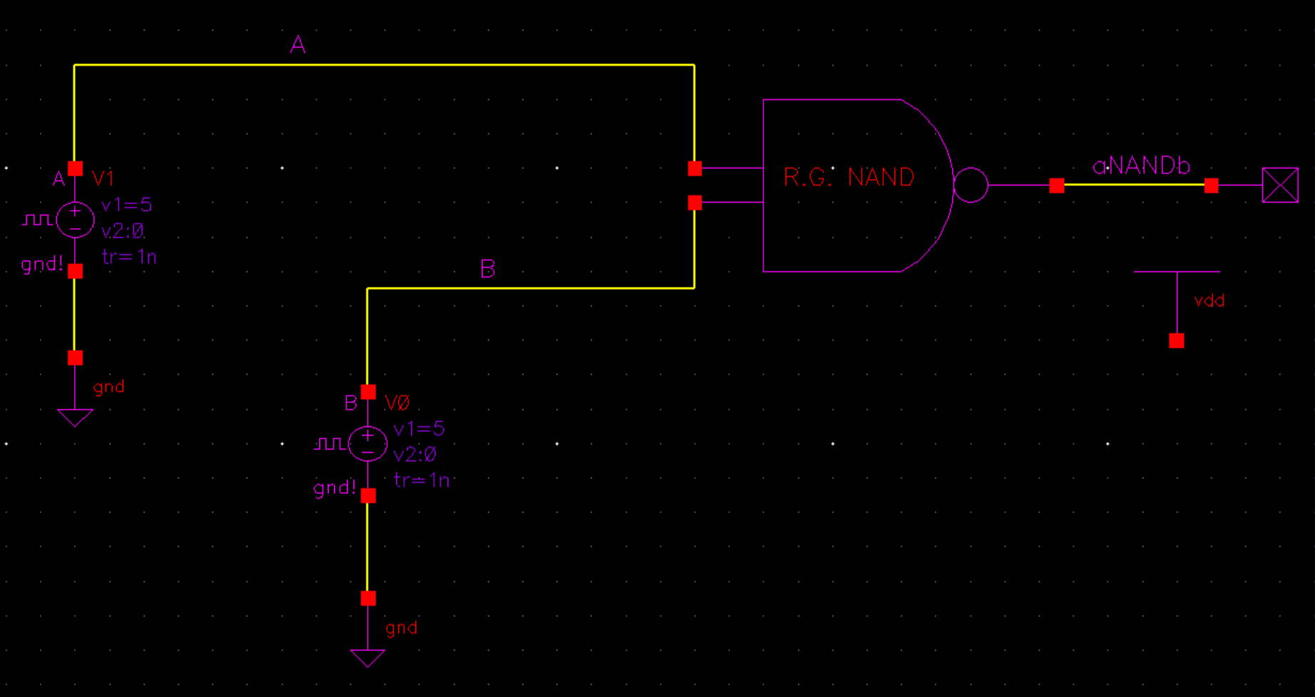 Circuit implementation |
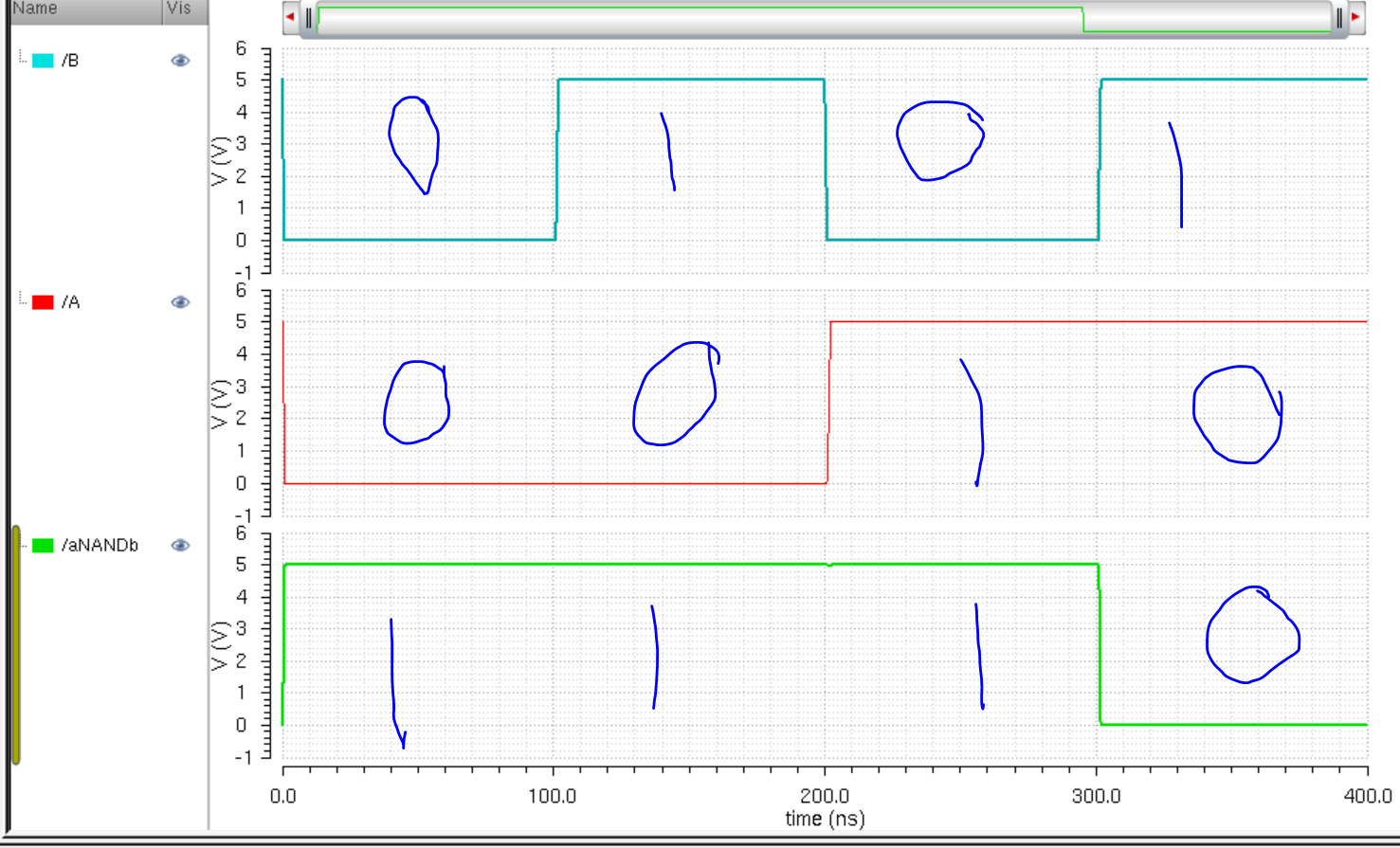 Results |
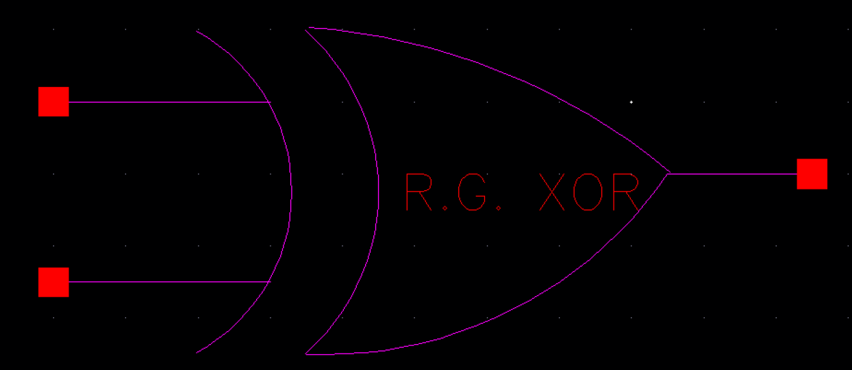 2-input XOR Symbol |
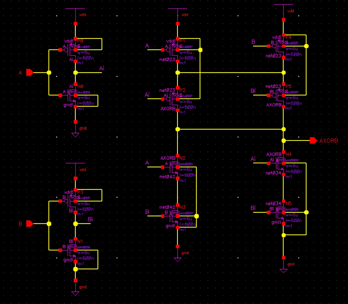 2-input XOR Schem |
2-input XOR Layout |
2-input XOR in a Circuit |
|
DRC Certification |
LVS Certification |
Circuit implementation |
Results |
File Back-up Proof