Lab 4 - EE421L
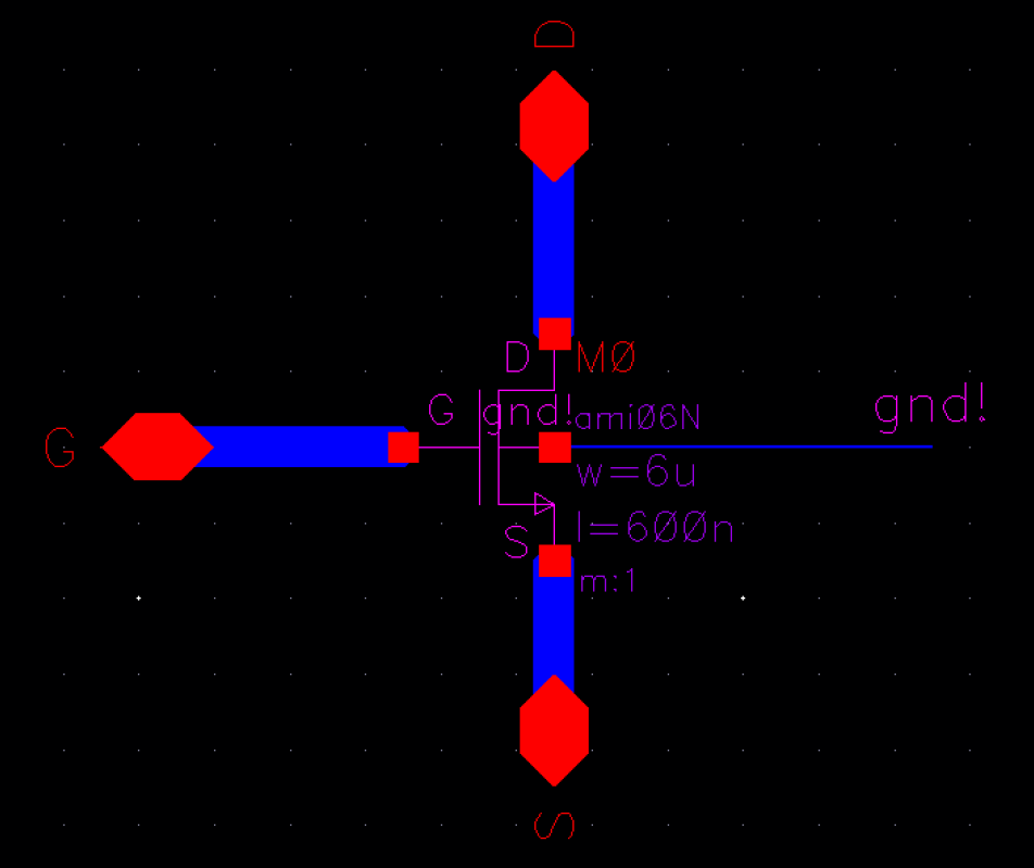
| NMOS schematic |
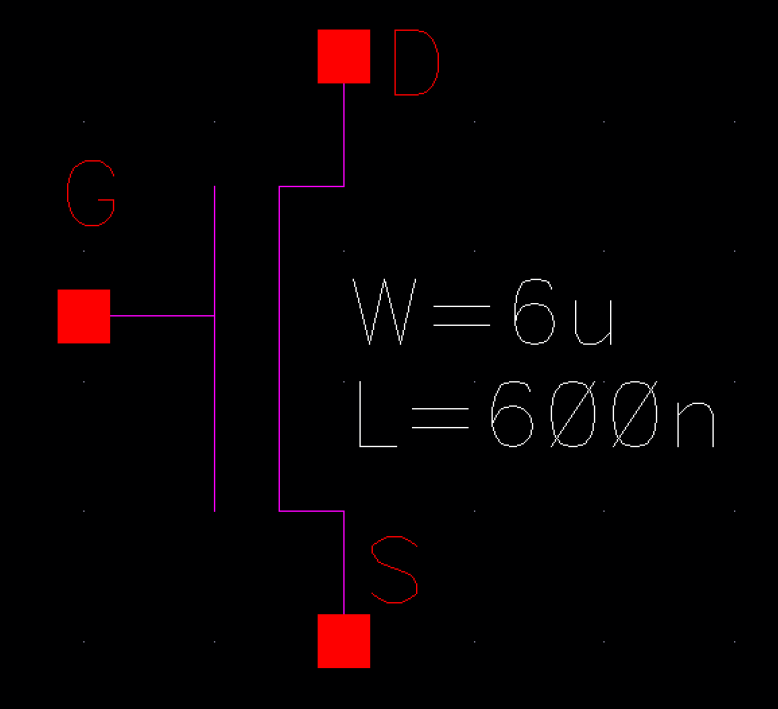
NMOS symbol |
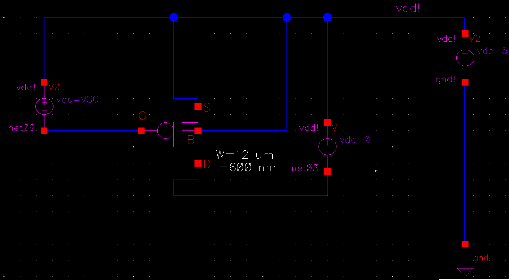
NMOS in a circuit |
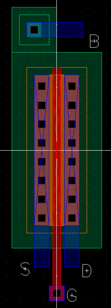
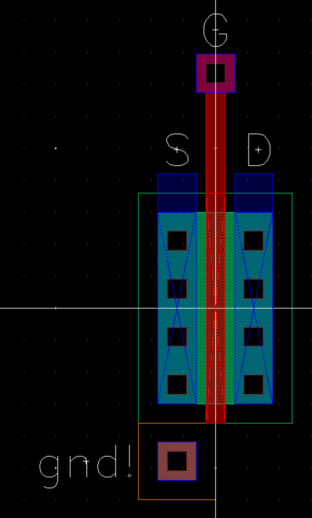
| NMOS layout |
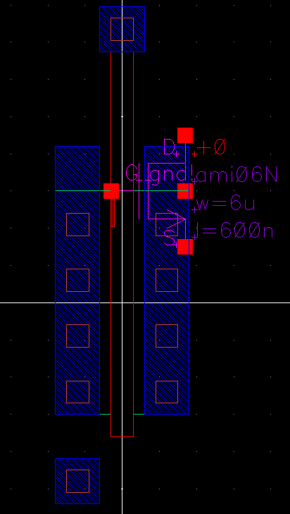
NMOS extracted layout |
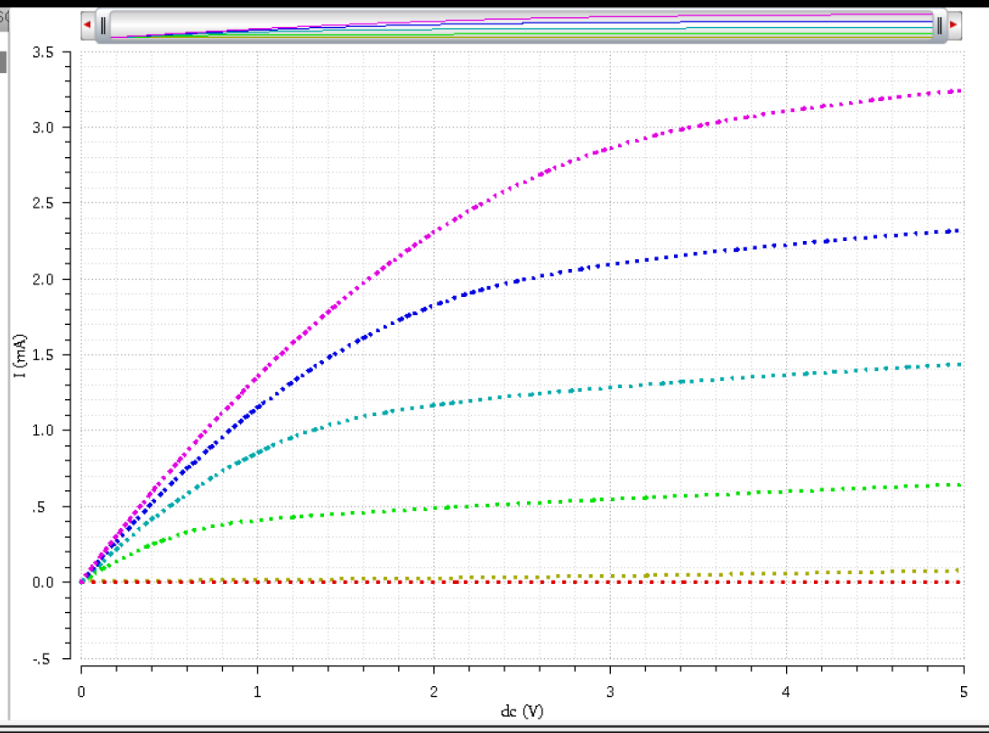
Simulation Results |
PMOS schematic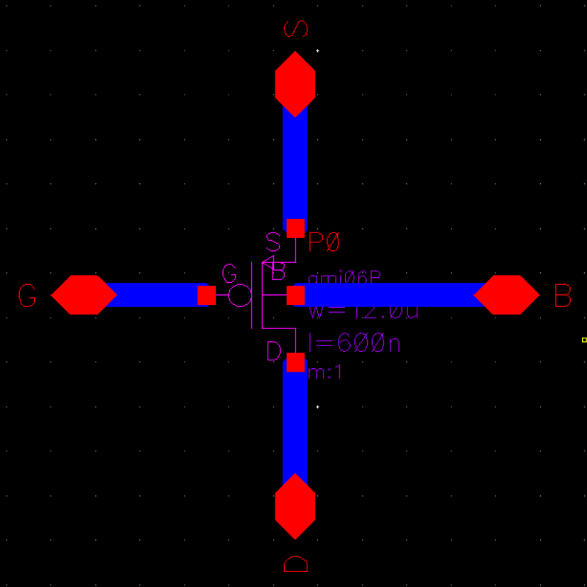 |
PMOS symbol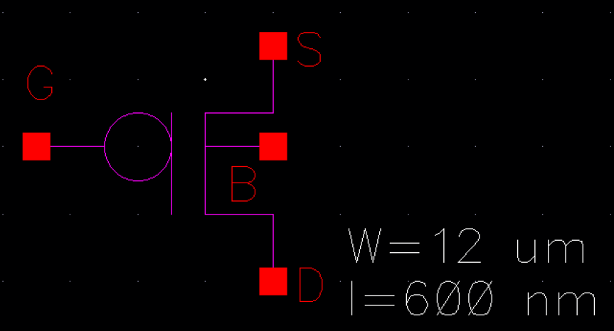 |
PMOS in a circuit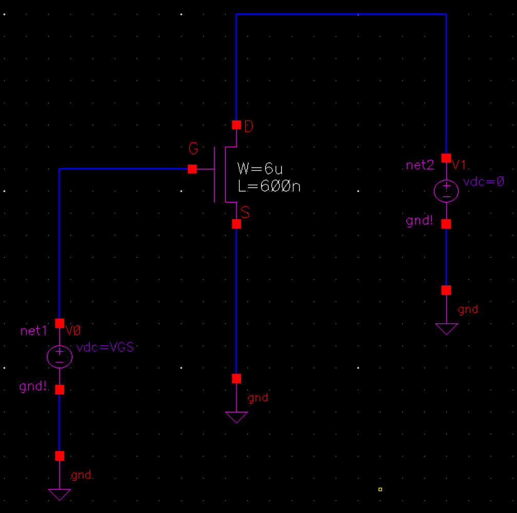 |
|
|
PMOS extracted layout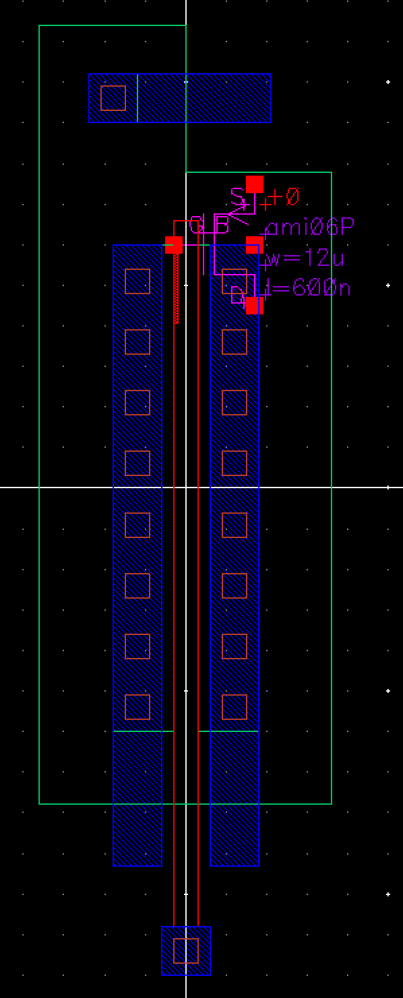 |
Simulation Results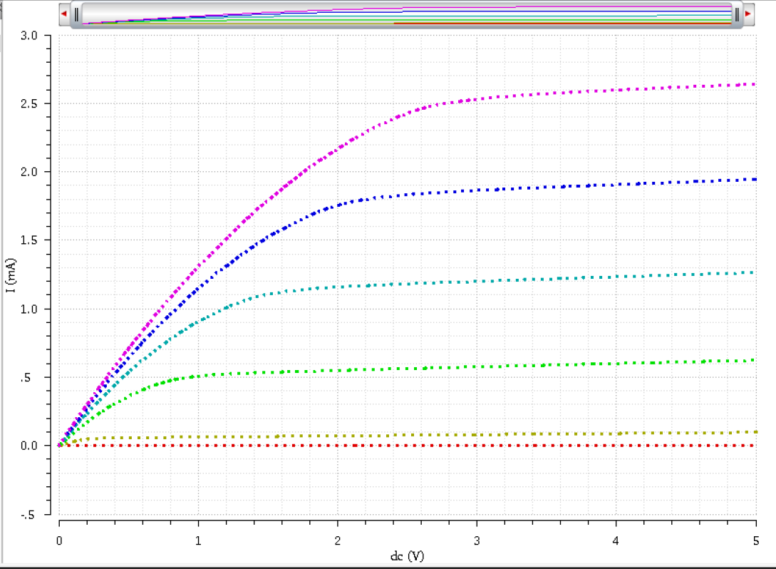 |
The Lab
1) Generate 4 schematics and simulations
NMOS ID vs VDS
SCHEMATIC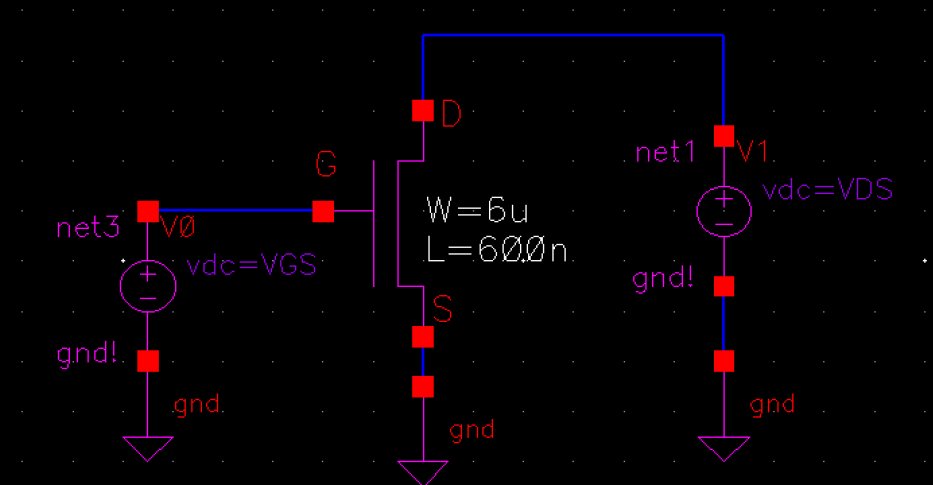 |
SIMULATION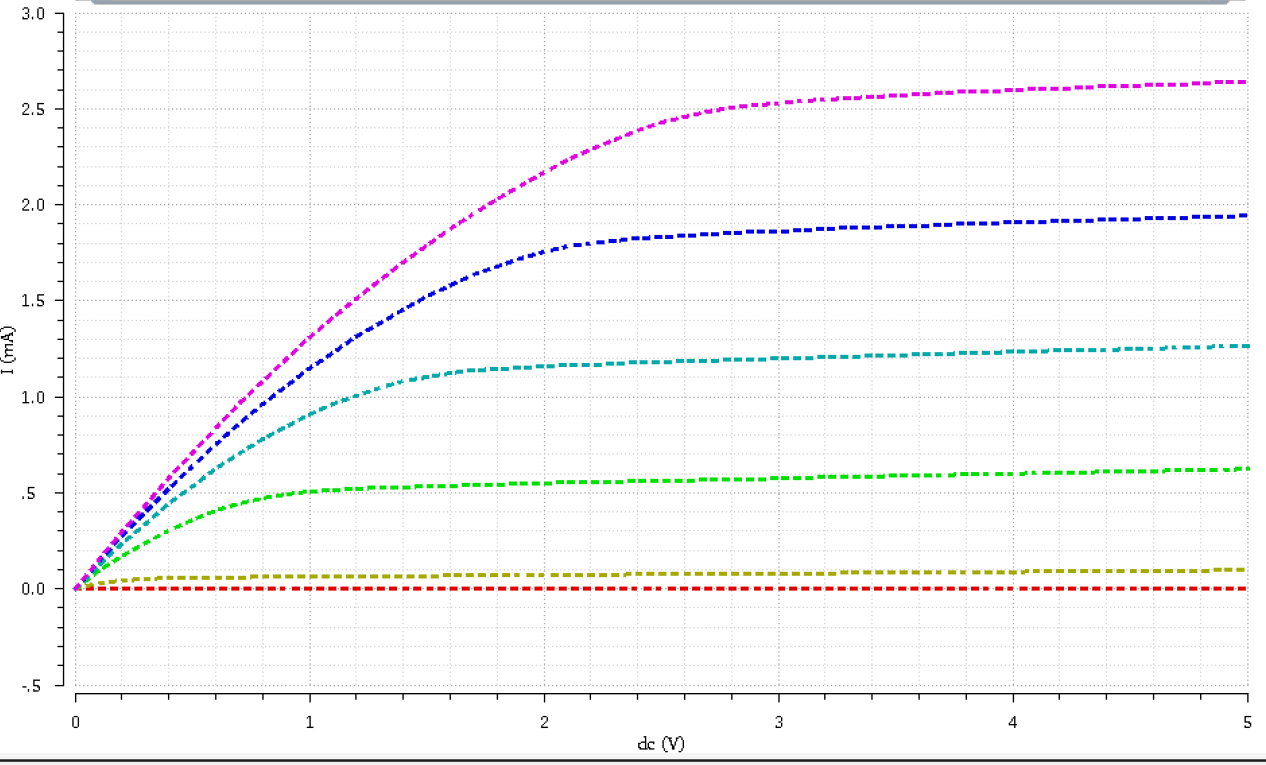 |
SCHEMATIC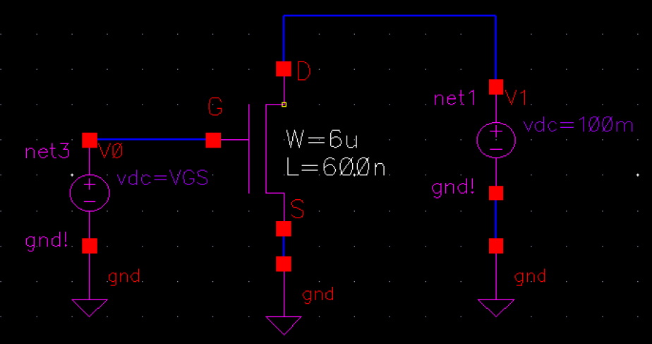 |
SIMULATION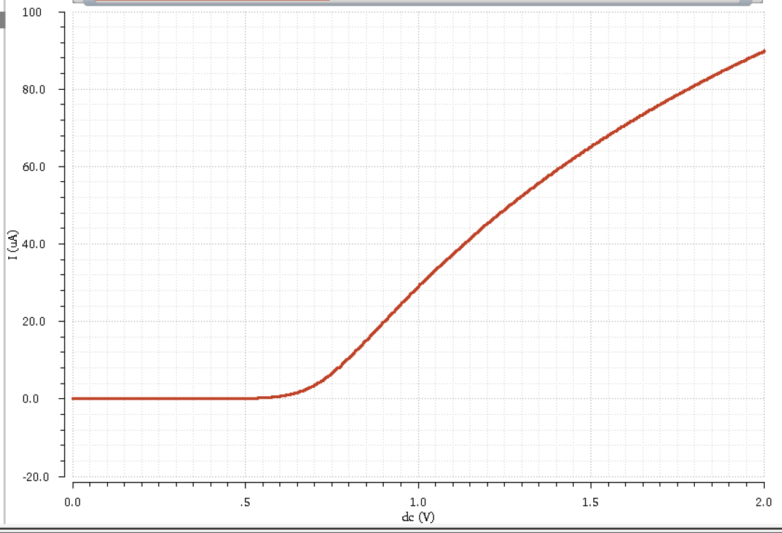 |
SCHEMATIC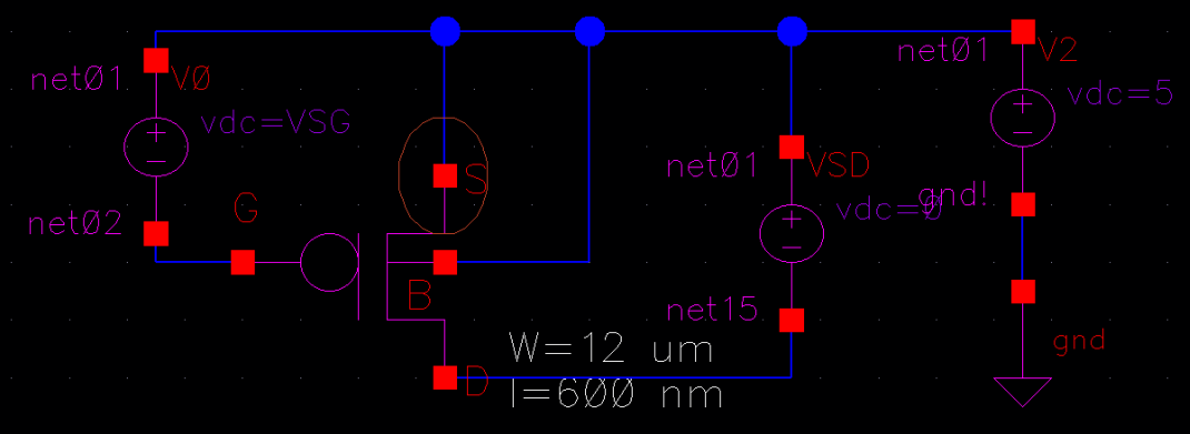 |
SIMULATION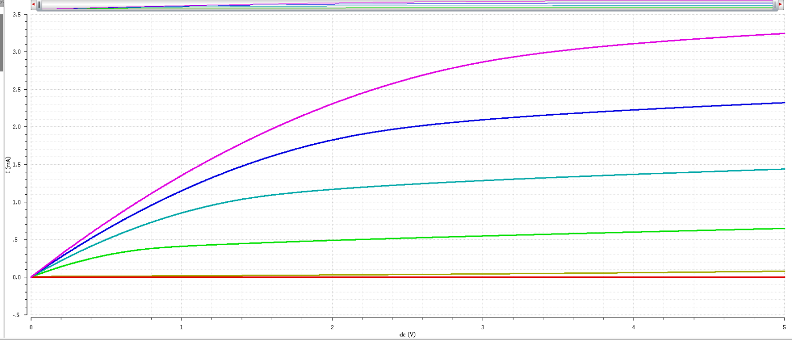 |
SCHEMATIC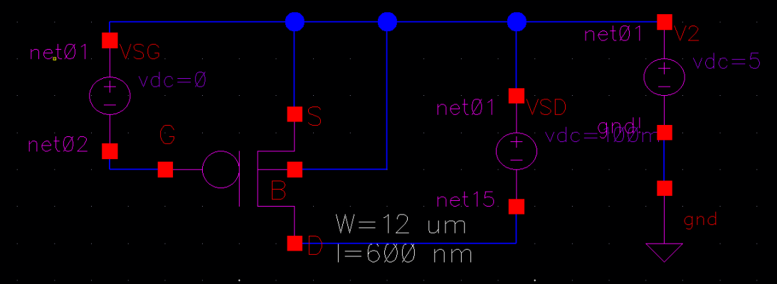 |
SIMULATION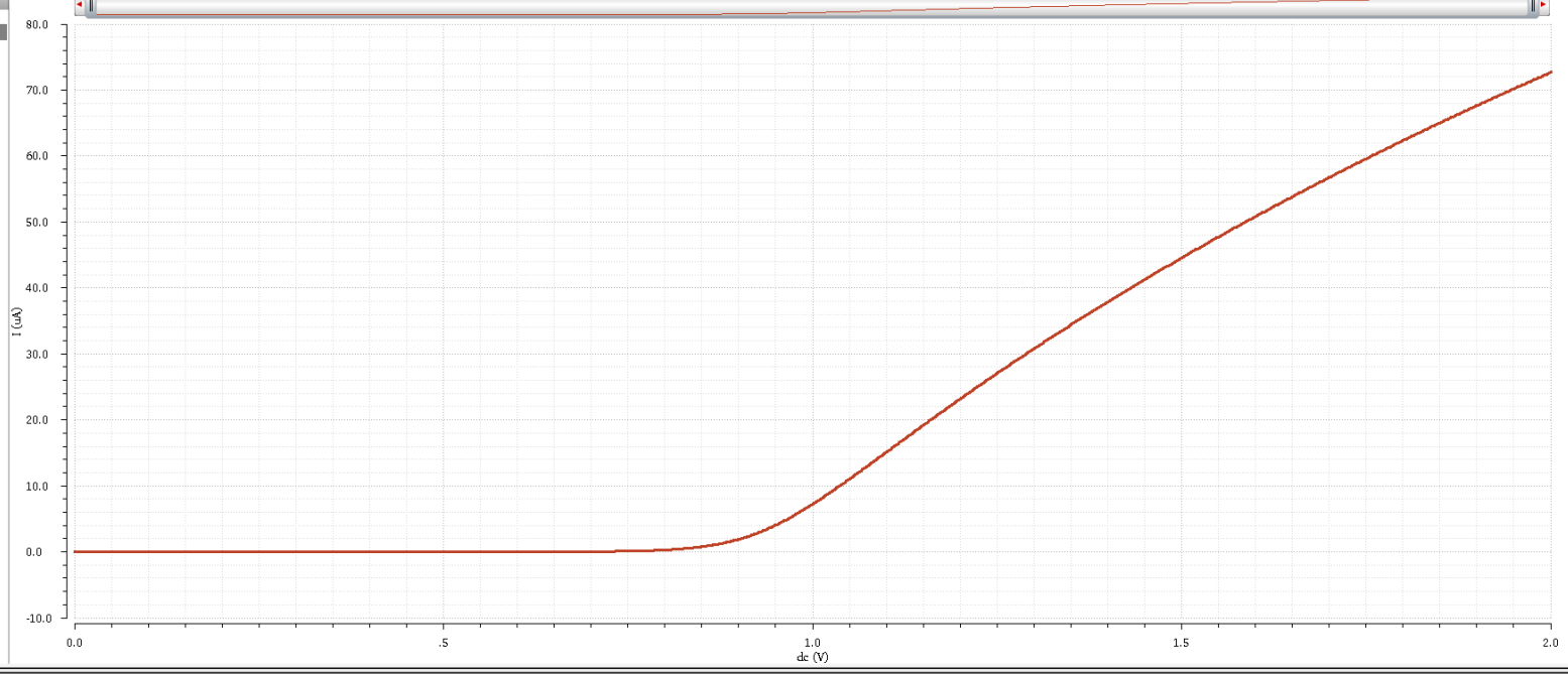 |
2) NMOS and PMOS with 4 probepads attached:layouts , schematics, DRC, and LVS confirmation
NMOS:
SCHEMATIC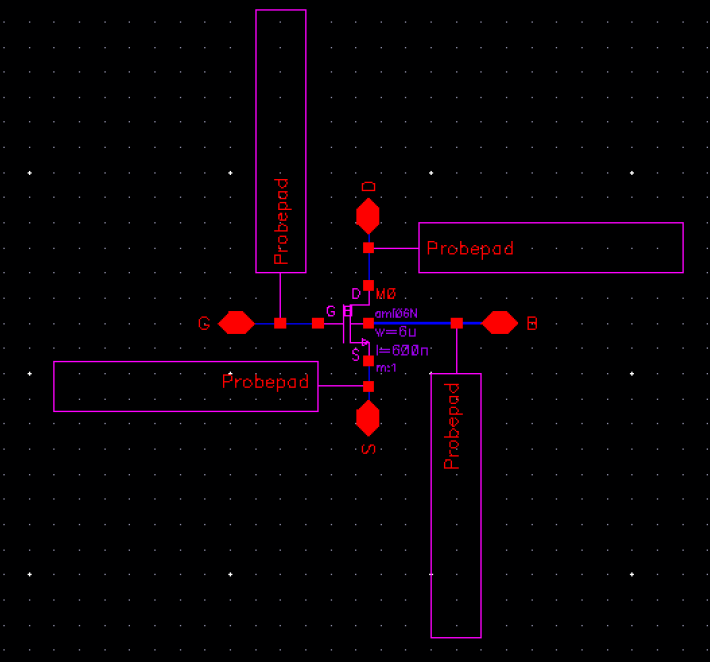 |
LAYOUTS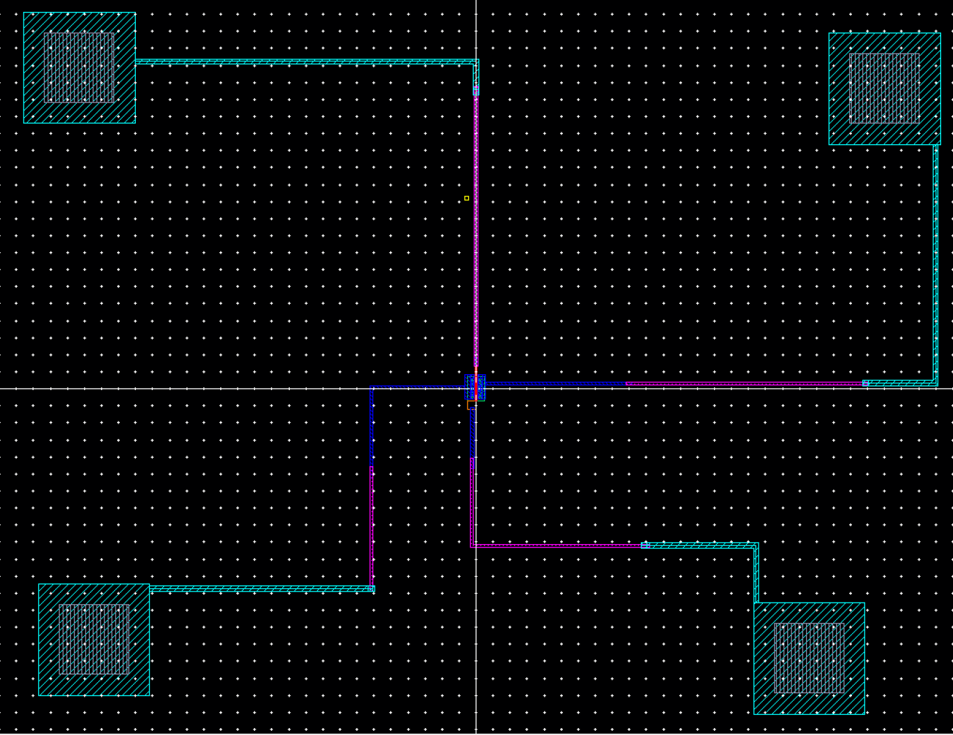 |
DRC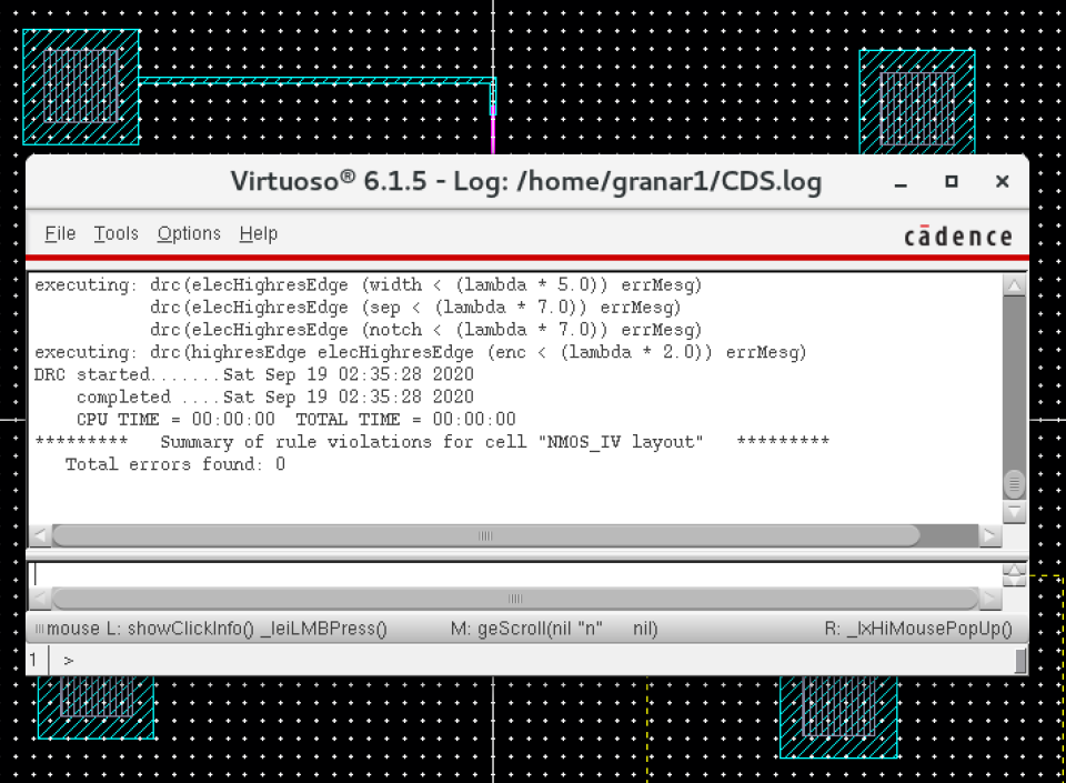 |
LVS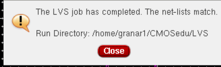 |
PMOS:
SCHEMATIC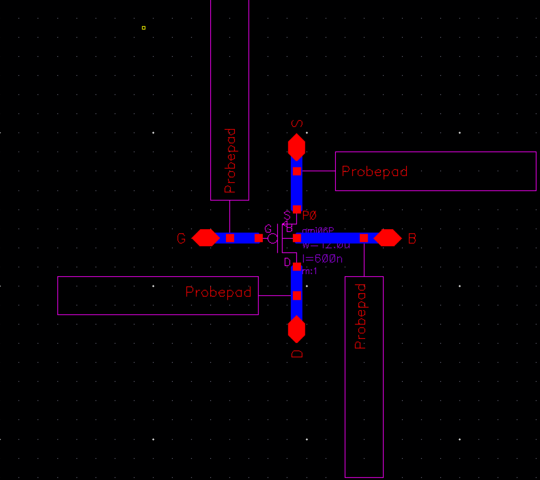 |
LAYOUTS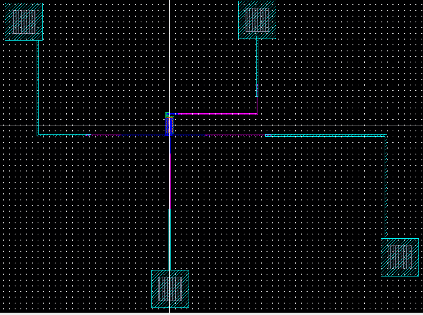 |
DRC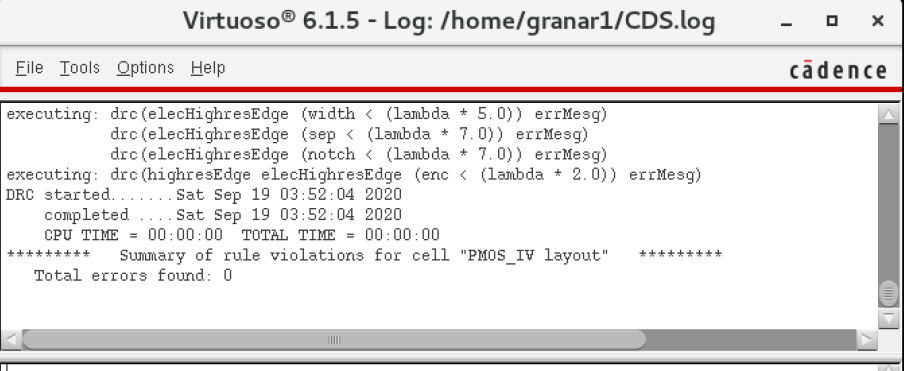 |
LVS |
File Back-up Proof