Lab 5 - ECE 421L
In this lab, we'll be using Cadence to layout and simulate a CMOS inverter.
Prelab:
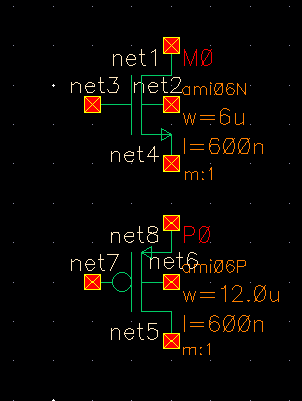
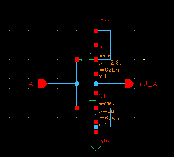
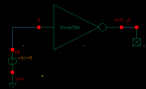
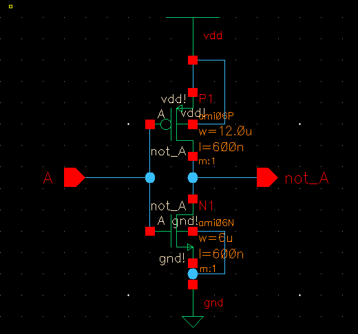
To start I instantiated a PMOS and an NMOS to connect them into an inverter as so:
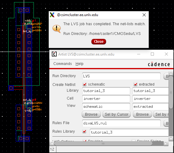
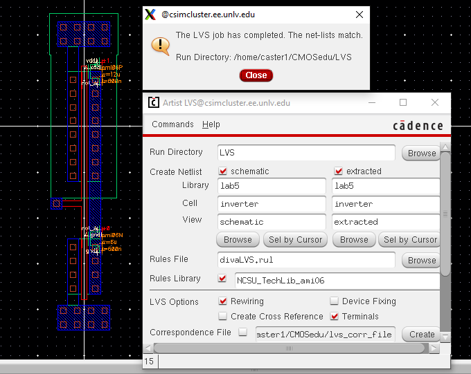
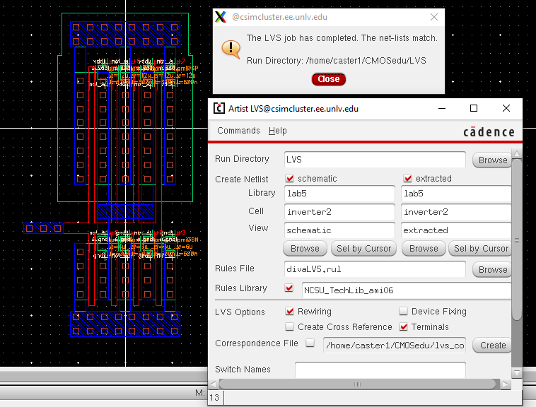
LVS:
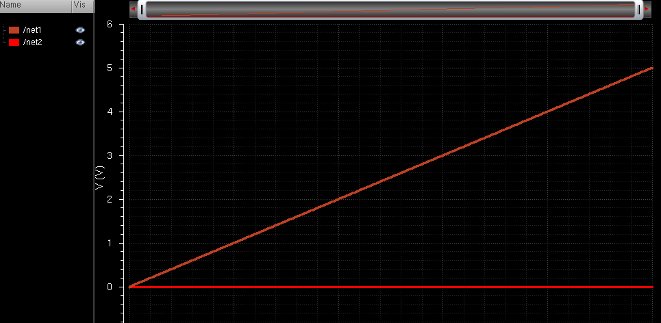
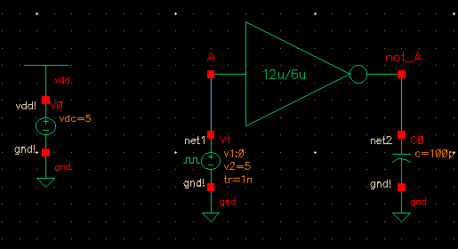
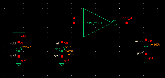
Schematic and Simulation:
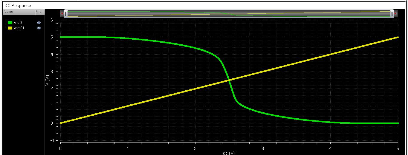
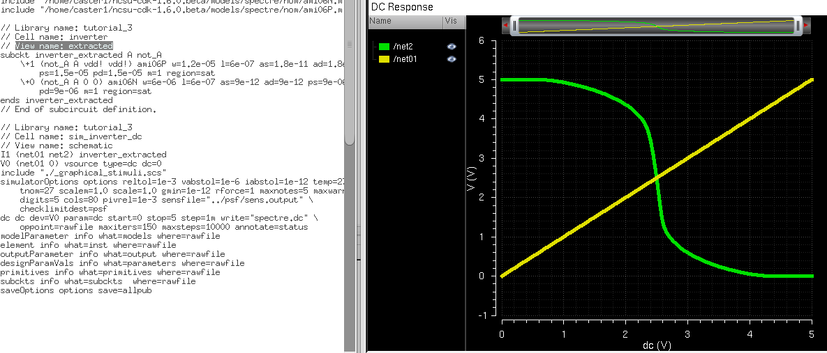
Finally, I ran the DC analysis on the schematic and the extraction:
Lab:
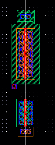
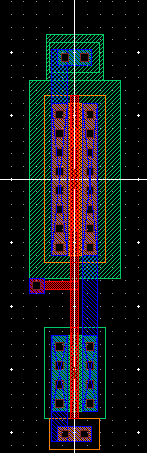
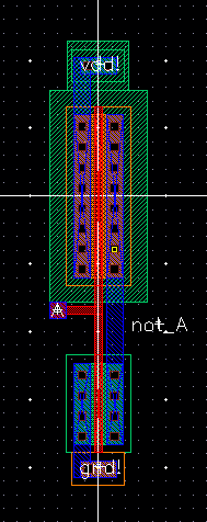
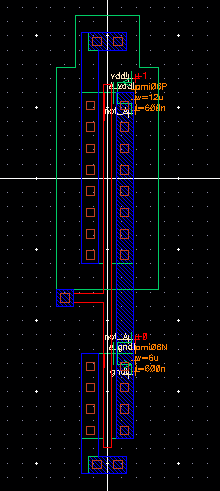
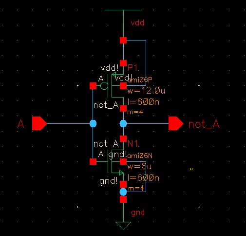
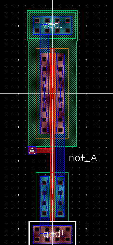
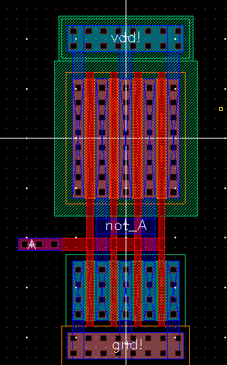
In the following screenshots, I show the layout, schematic, and extraction of the 12/6 and the 48/24 inverters side by side (along with the LVS). I did not have any significant difficulties getting the layouts to work.
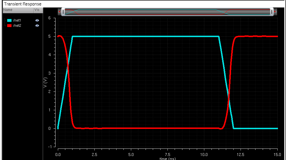
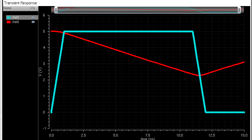
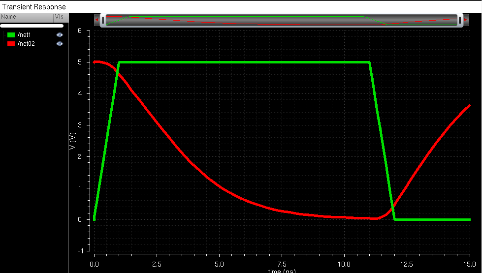
The next side-by-side images show the schematics for the testing circuits, the Spectre simulations, and then the UltraSim simulations:
Spectre:
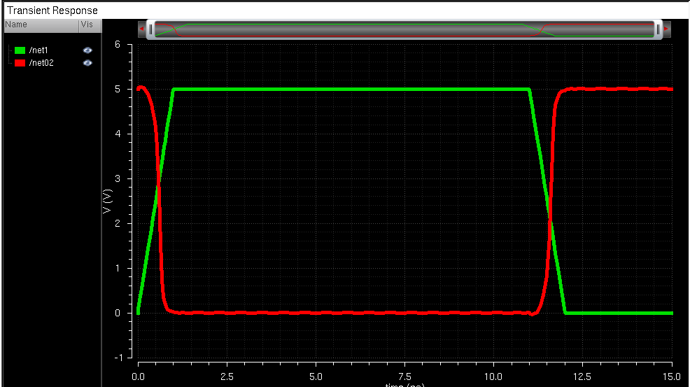
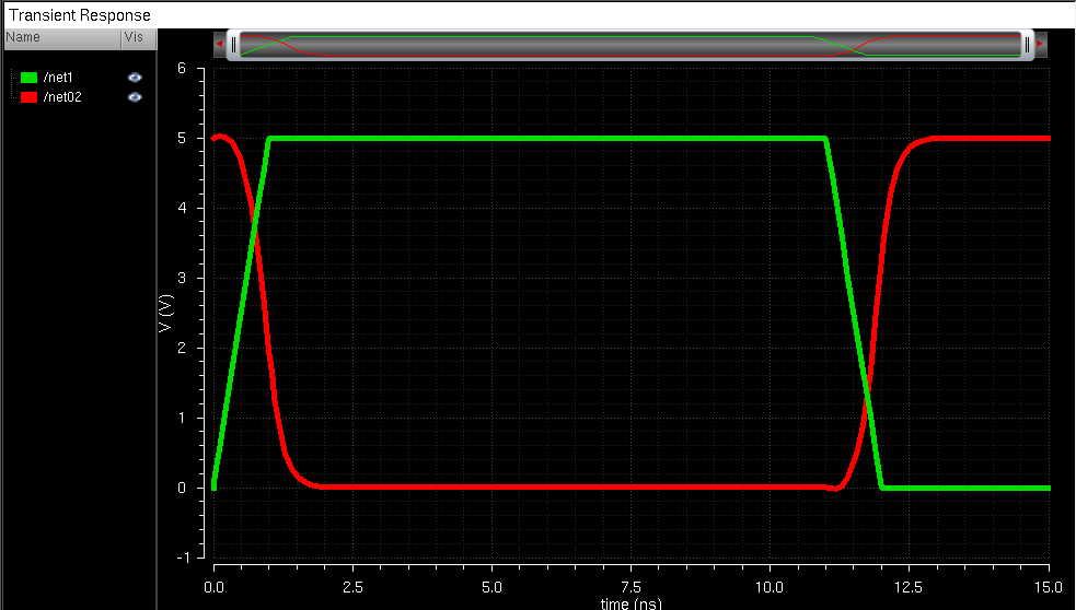
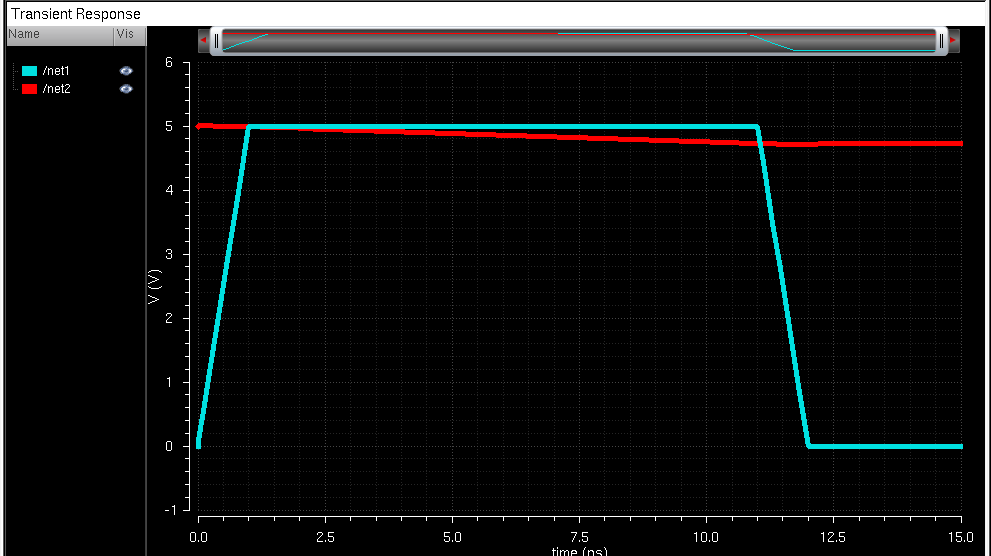
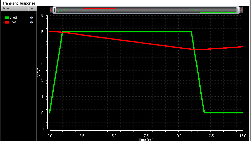
Ultrasim:
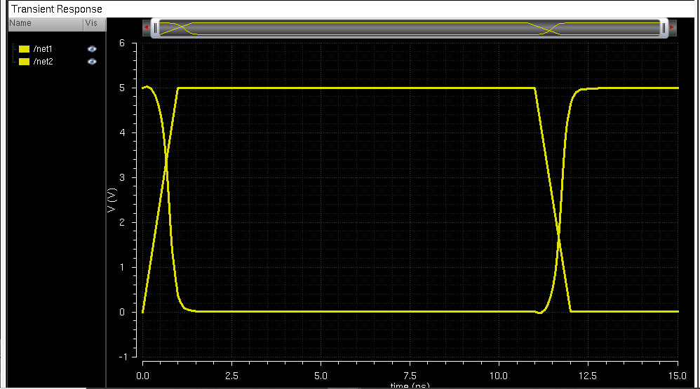
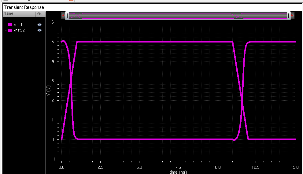
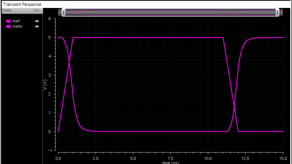
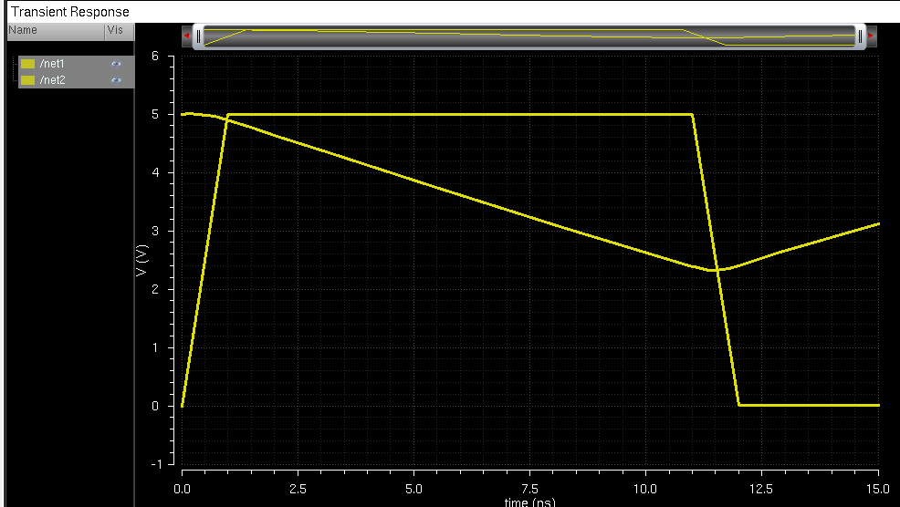
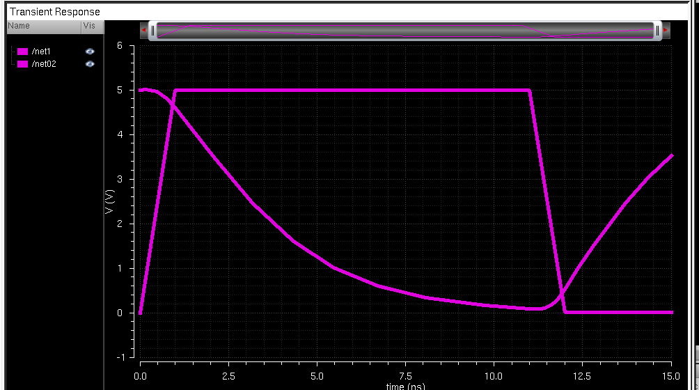
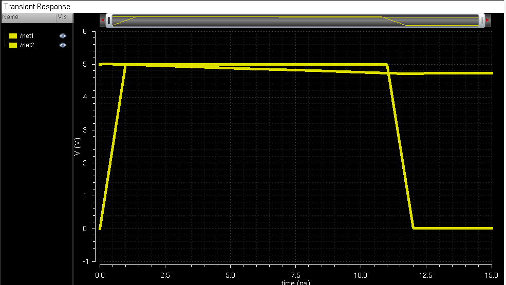
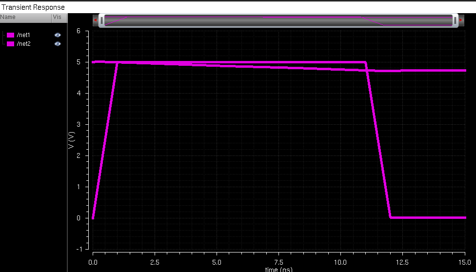
It is apparent that the two different simulation engines provided the same results.
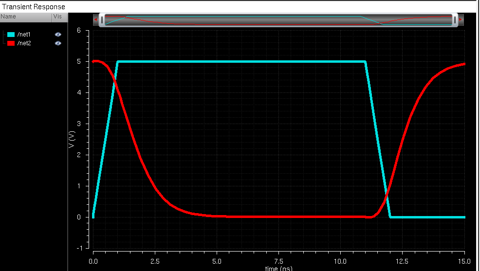
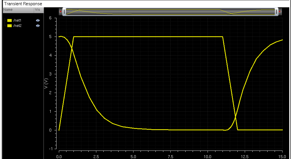
The reason that the output becomes flatter and flatter as the capacitance gets higher because the capacitor is "smoothing" it out. It stores charge when the output signal is high (and, by nature of the inverter, when the input is low) and discharges when the ouput is low (and the input is high).