Lab 4 - ECE 421L
Authored
by Ryan Castellano
September 22, 2020
Lab Description:
In this lab, we'll be learning the design, layout, and simulation of PMOS and NMOS transistors.
Prelab:
For
the Prelab, we were required to complete tutorial 2. In tutorial 2, we
simulated both PMOS and NMOS transistors that we layed out and desgined
symbols for ourselves. The following images show, in order, the
following:
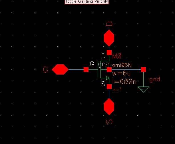
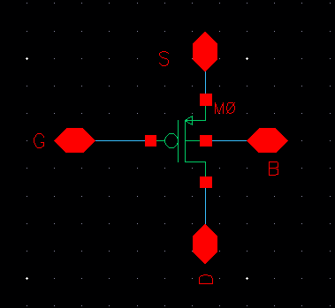
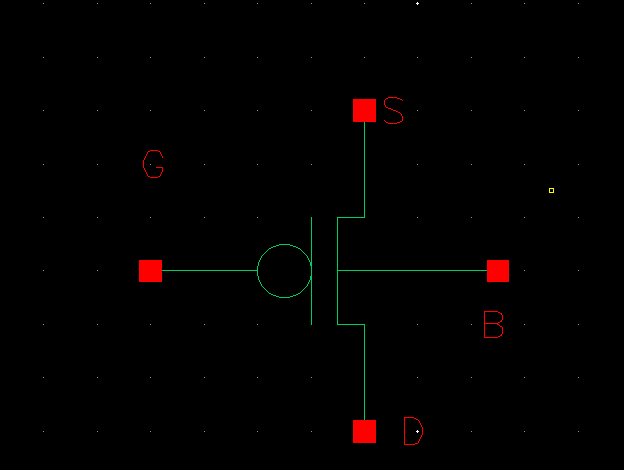
1. The creation of the schematic and symbol for an NMOS
2. The creation and simulation of a testing circuit for an NMOS
3. The process of eliminating the design errors
4. The simulation of the testing circuit and the extracted view
5. The same steps for the PMOS (barring the planted errors from the first part)
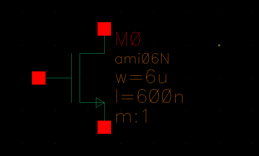
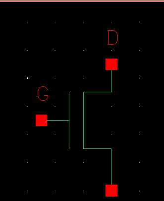
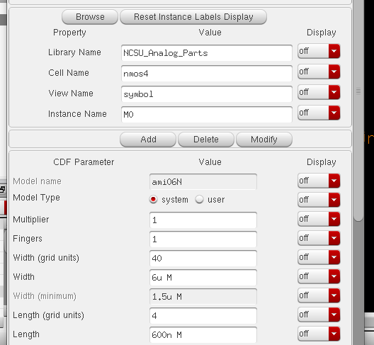
Symbol:
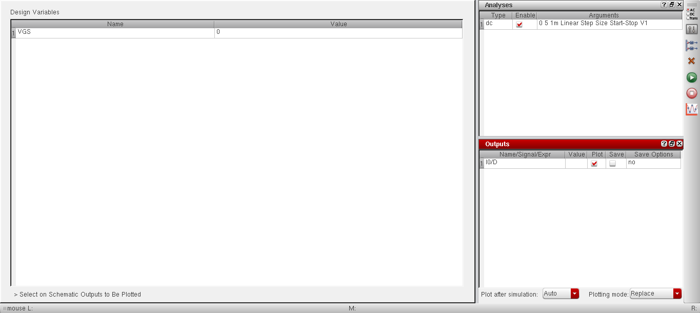
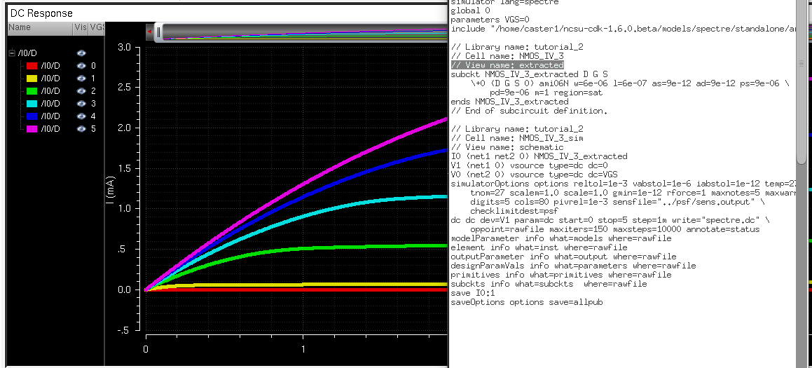
Sim settings:
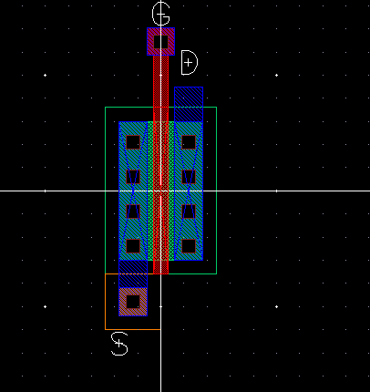
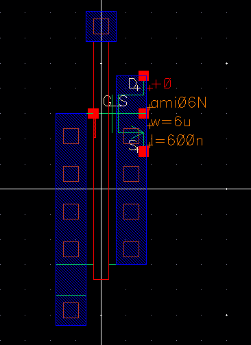
Layout and Extraction: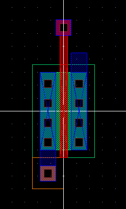
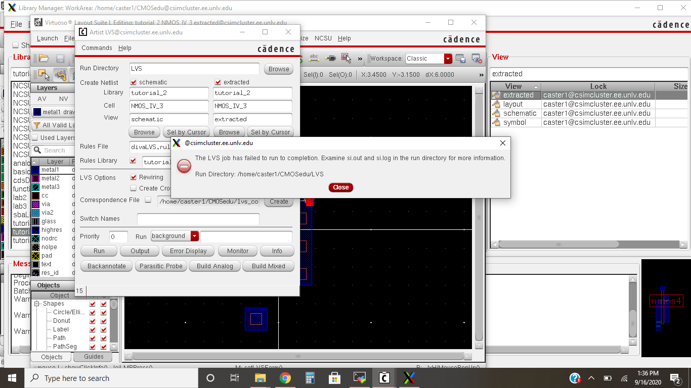
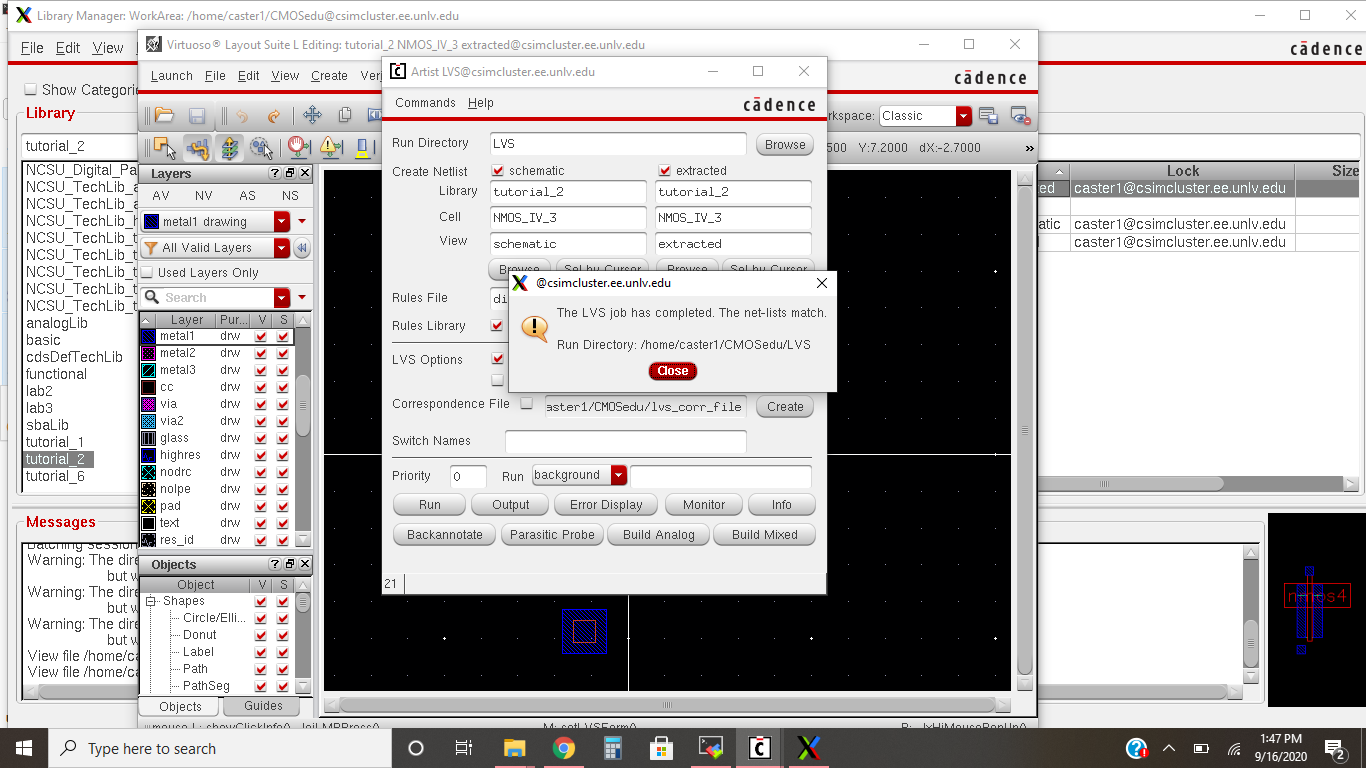
LVS fail:
LVS Success:
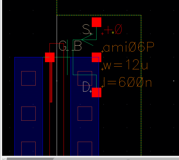
PMOS Schematic, symbol and layout:
More layout and extraction:
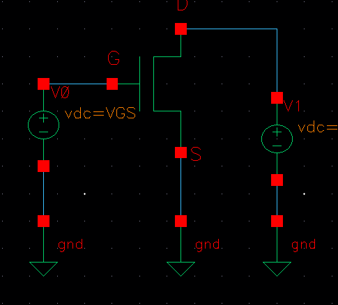
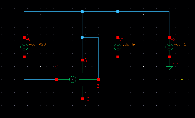
Testing schematic and extraction:
Lab:
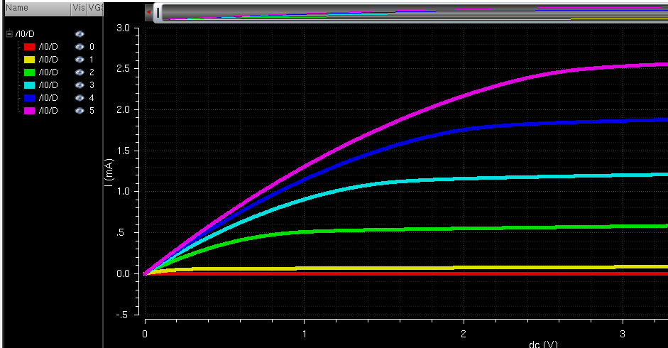
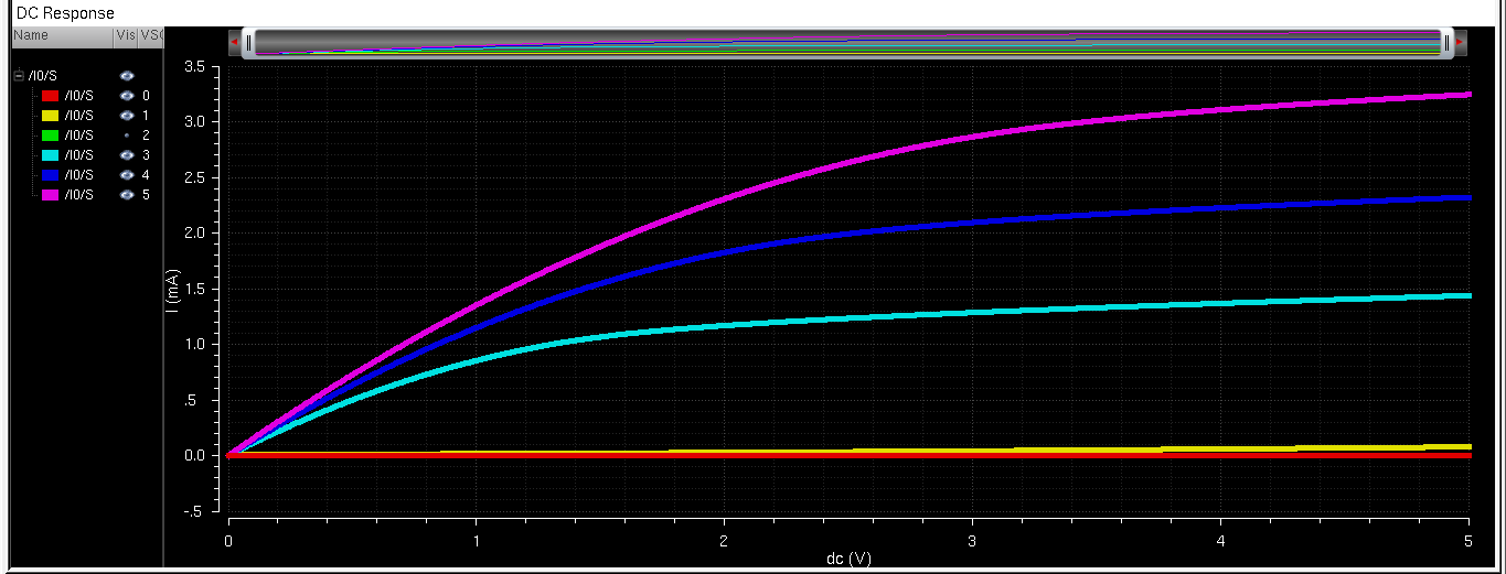
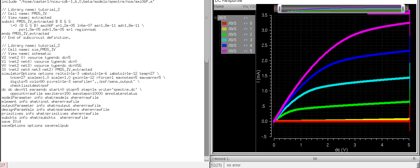
Both
simulations for the VDS varying from 0 to 5 were already done in the
prelab ( shown in the transient simulation settings in the pictures
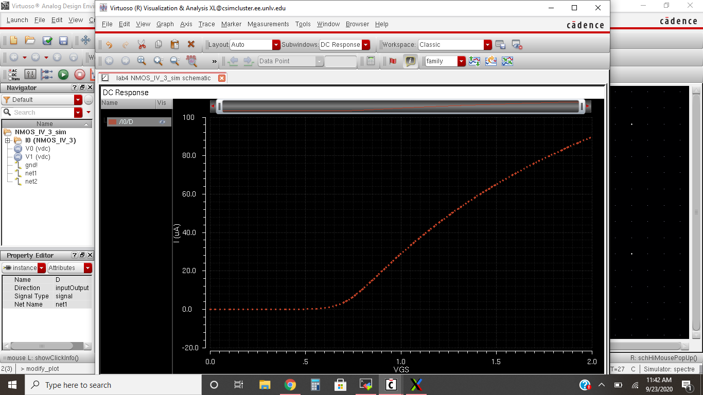
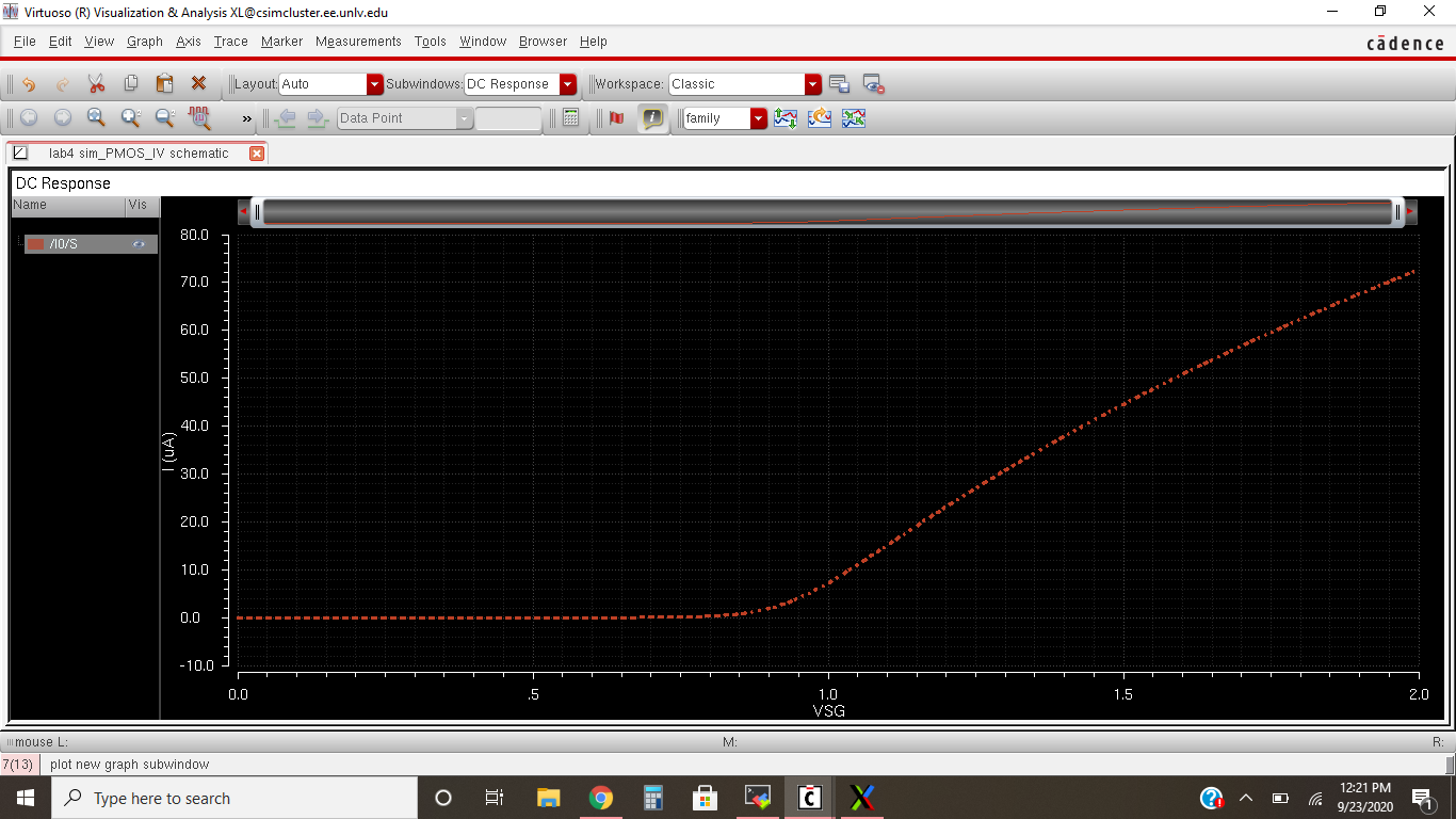
above). The simulations for the 1mV steps from 0 to 2 volts for both
the PMOS and NMOS are shown below:
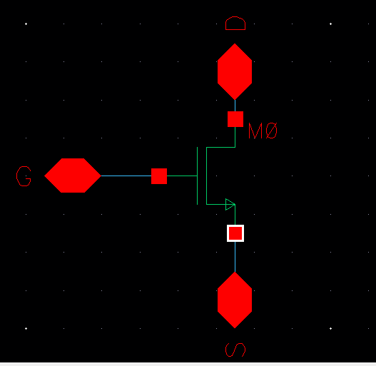
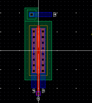
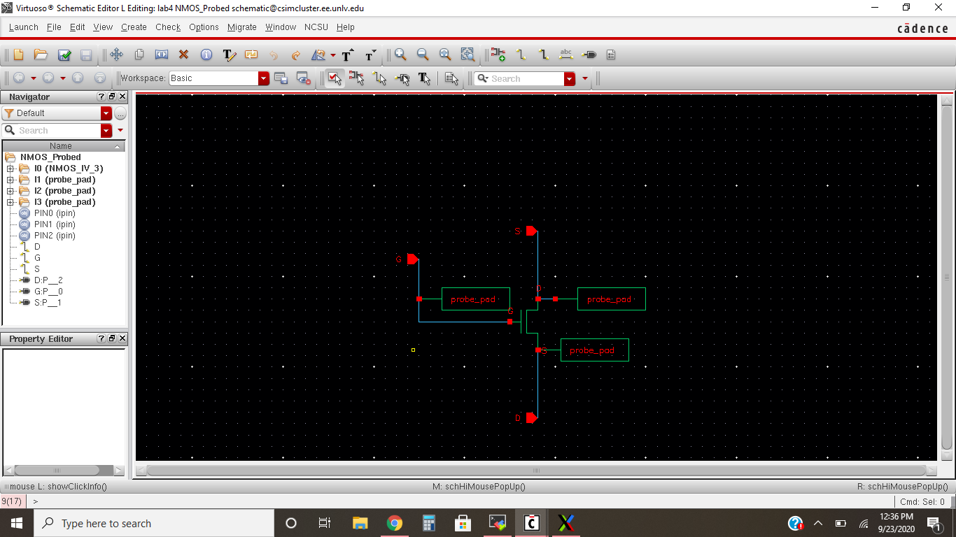
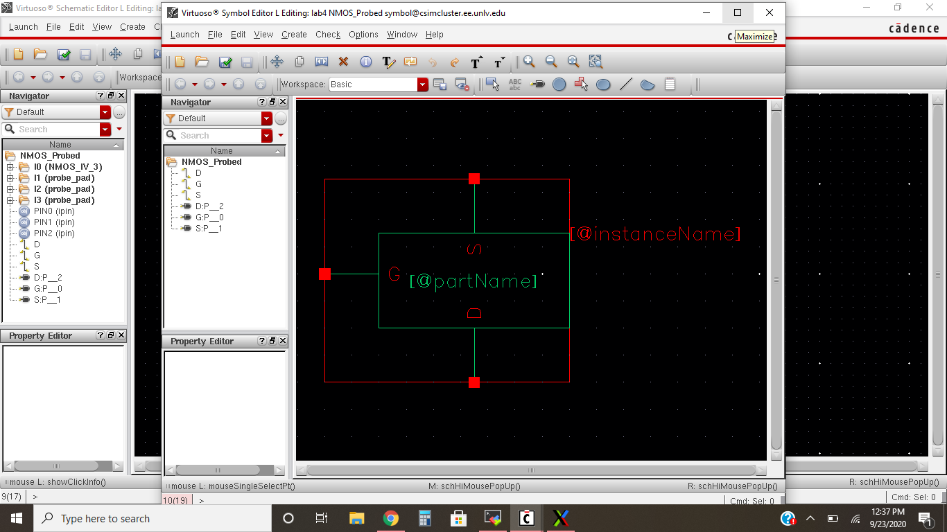
The pad and symbol for the NMOS is shown below:
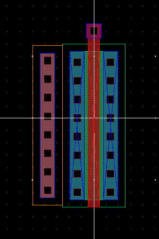
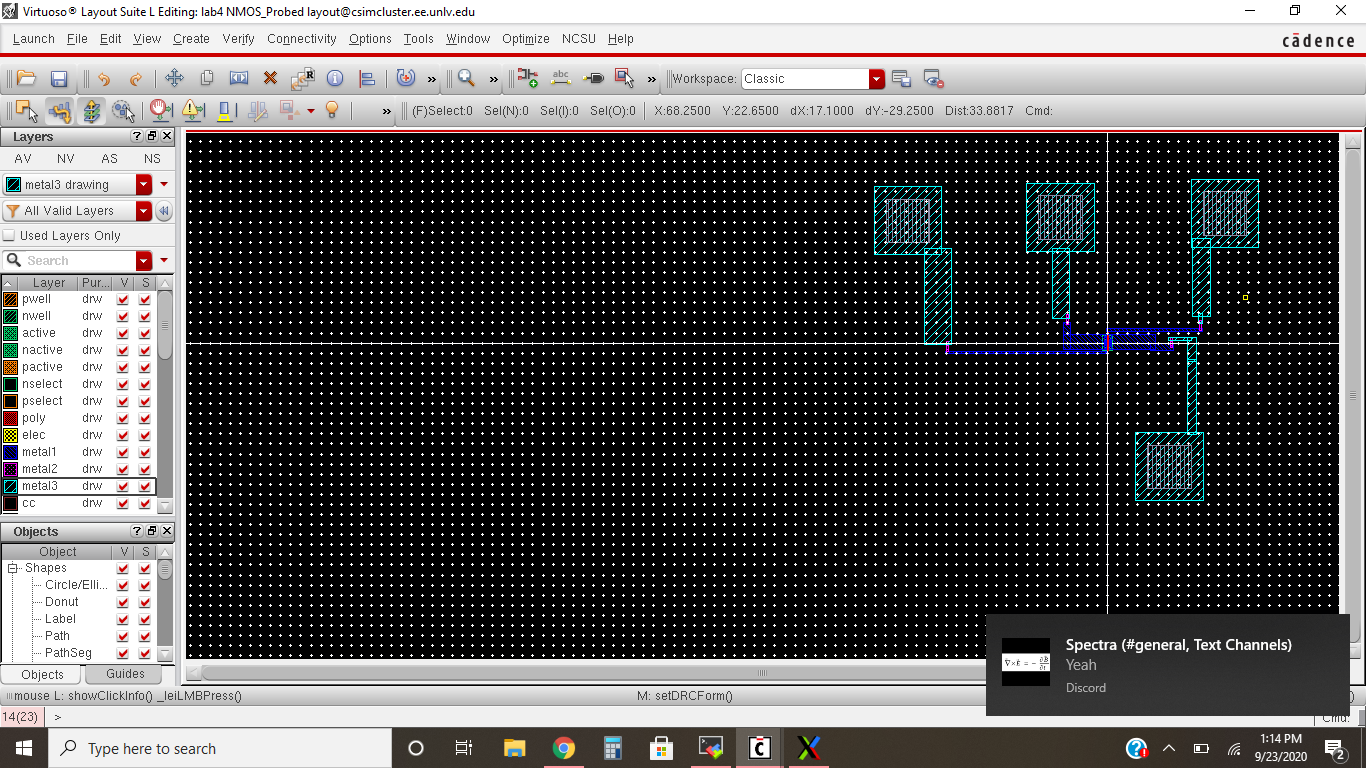
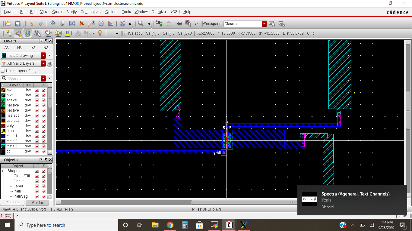
The
layouts are shown below. They DRCed and LVSed properly, as it did when
I did the same steps for the PMOS (though the were already done in the
lab4.zip).
Return to EE 421 Labs