Lab 3 - ECE 421L
Authored
by Ryan Castellano
September 9, 2020
Lab
description
In this lab, I will be using the layout system in Cadence to recreate the DAC from the previous lab.
Prelab
As
per the prelab instructions, I finished tutorial 1 starting from
screenshot 25 (where we left off in the first lab). I started by
removing the voltage source and adding pins. Then I clicked create
symbol which gave me the first symbol and I drew the final one. I
simulated the results to make sure it still worked:
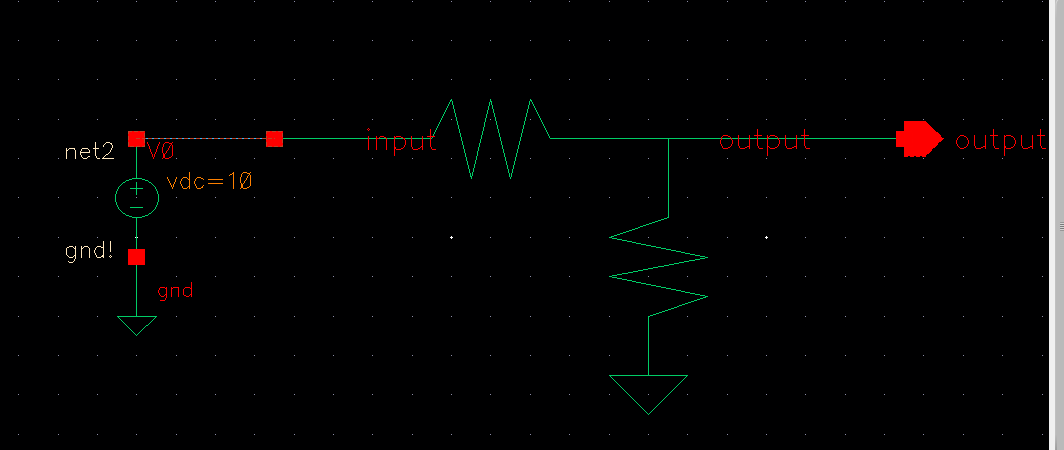
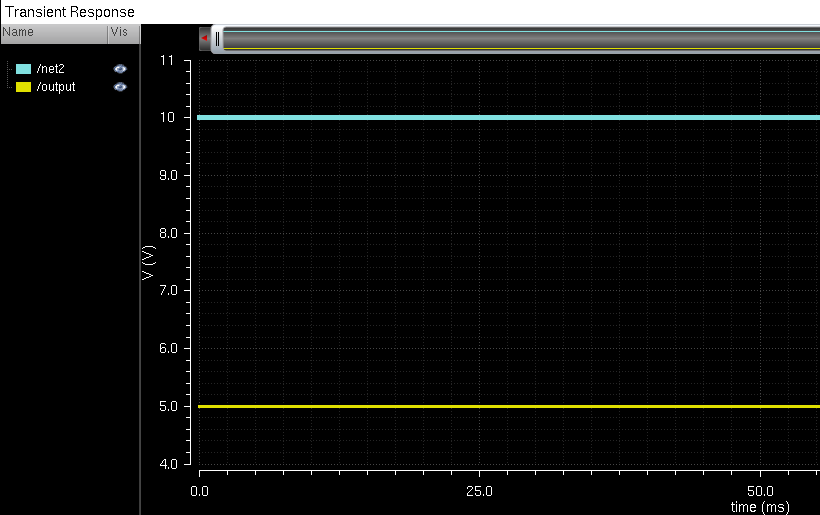
With
the schematic done, I moved on to the layout. In the first image, I
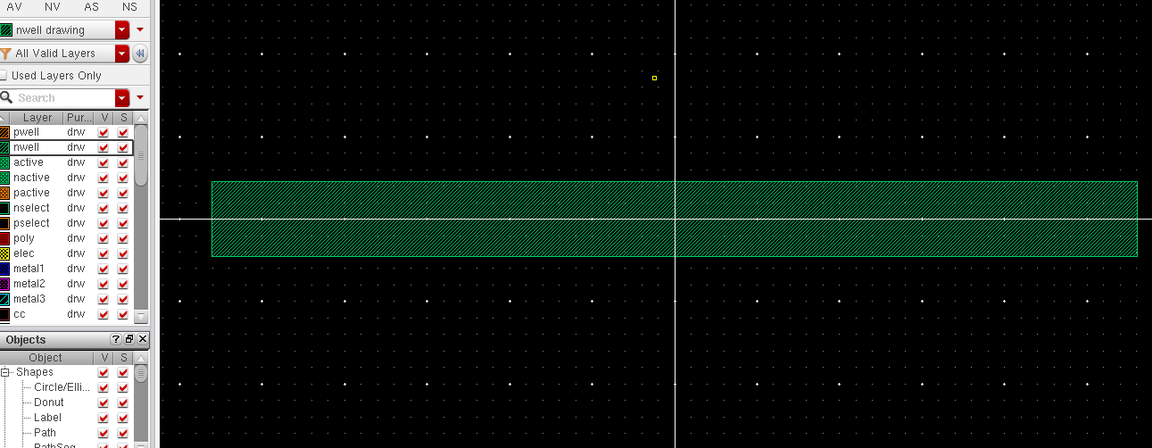
created a PMOS rectangle with length of 56.1 microns and a width of 4.5
microns. This was created by assuming that the average sheet resistance
was 800 ohms. Also, MOSIS design process specifies the minimum width is
3.6 microns. So to calculate the resistance, we multiply the average
sheet resistance by the quotient of the length and the width. 800 *
56.1/4.5 = 9,973 ohms.
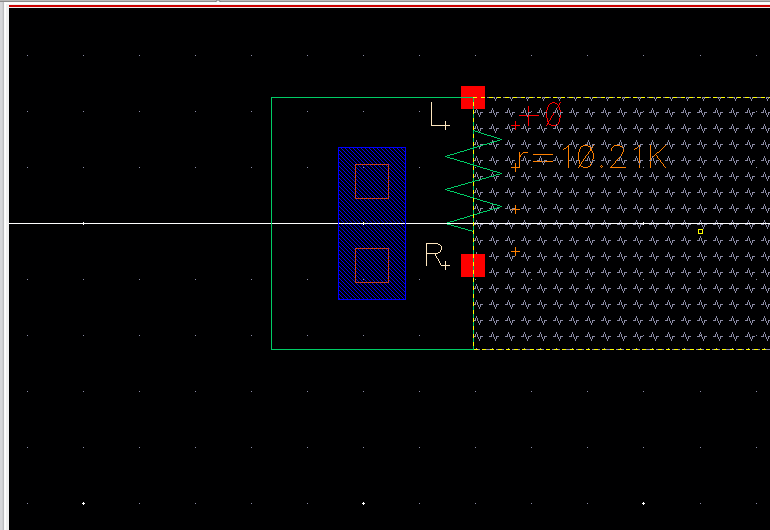
After
creating the rectangle, I added the taps, the metal, and the pins. I
then extracted the layout to see the resistance. The result is shown
below:
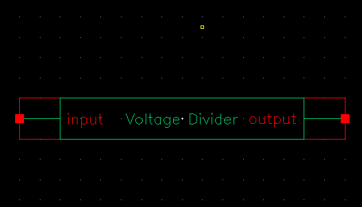
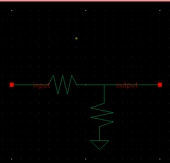
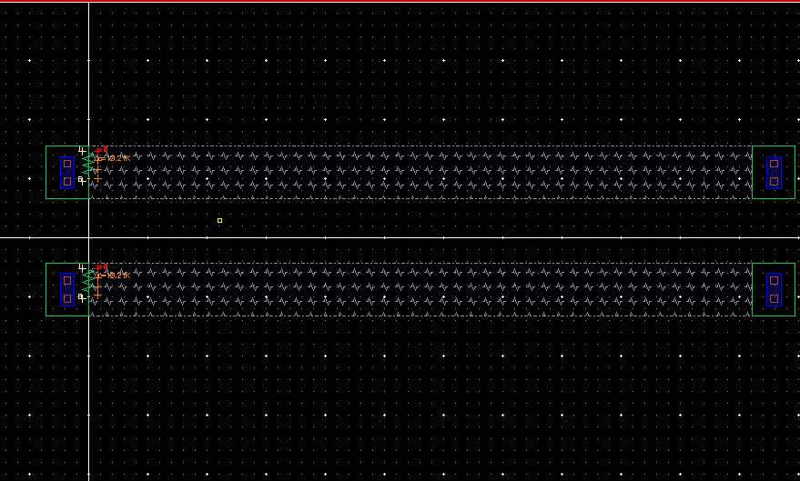
Next,
I created the layout for the voltage divider. I instantiated two
resistors and connected them together with a metal layer, and then
added pins. Then finally I DRCed and LVSed the layout. The results of
this are shown below:
 Lab
Lab
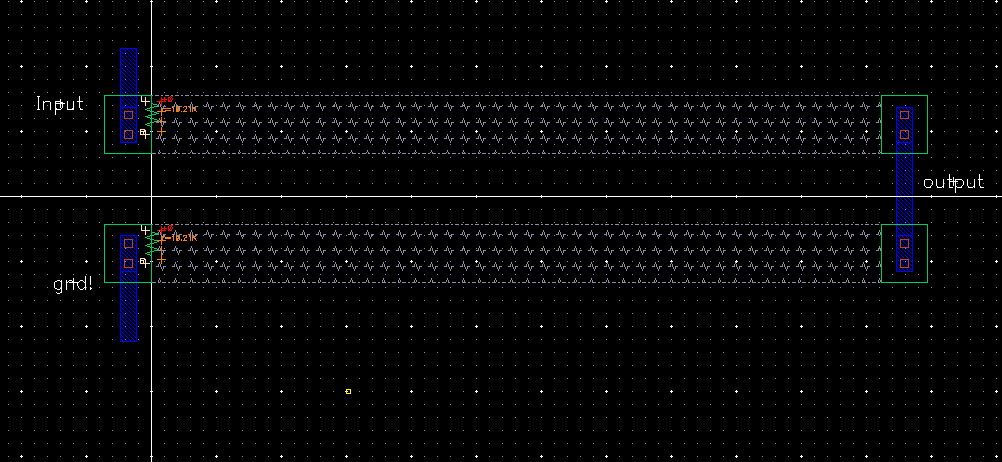
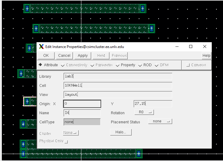
For
the resistor, I used the 10k ohm from the prelab and copied it into the
lab 3 directory. The design process was discussed above. I used the
property editor to set the length and width of the resistor. The full
length with the caps can be measured with the ruler feature. To make
sure that all of the resistors were 100% in parallel, I used the
property editor after I instantiated the resistors and set the
x-position at the origin.
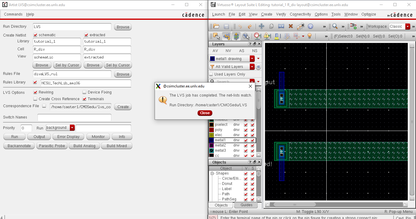
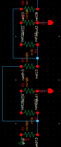
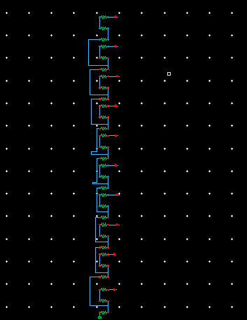
I created the DAC by connecting all
the resistors in the proper order with metal1. Then I created a circuit
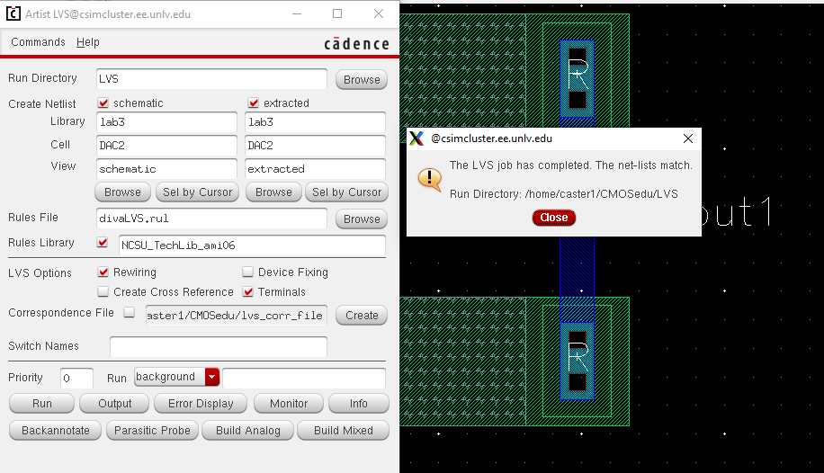
schematic to accompany my new DAC. I ran the LVS on these two systems
and the results showed that the netlist matched.
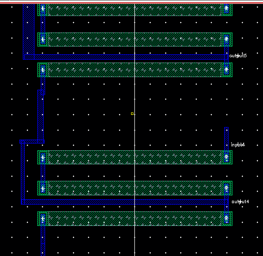
I
made the layout and the schematic by instatiating a bunch of resistors
randomly and then connecting them. The following images show the zoomed
out and zoomed in views, followed by the LVS.

My zip file is in the Lab 3 directory.
Return to EE 421 Labs