Lab 2 - ECE 421L
Prelab
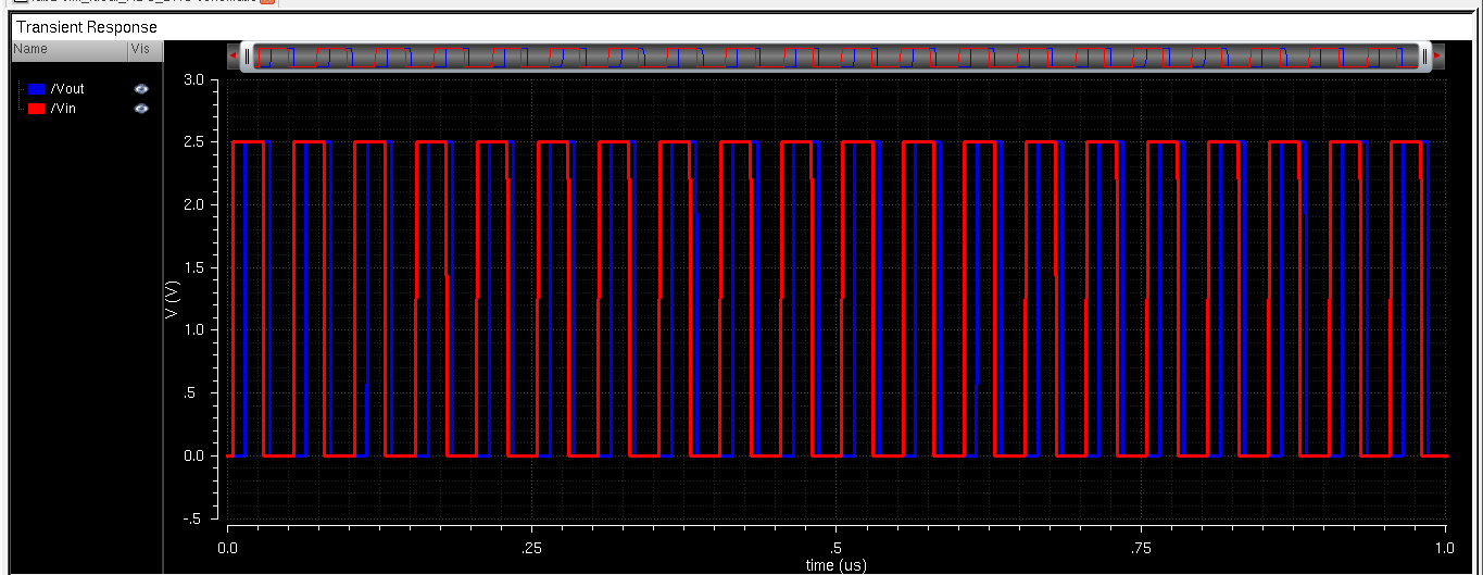
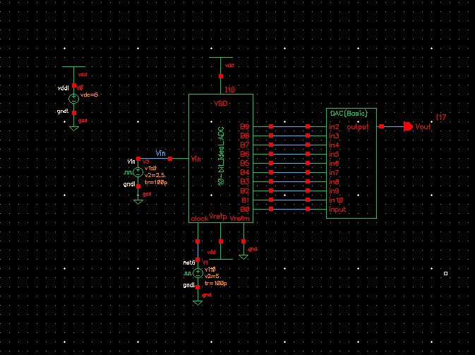
I downloaded the lab2.zip and added it to my Cadence library. After opening the file and running the simulation,
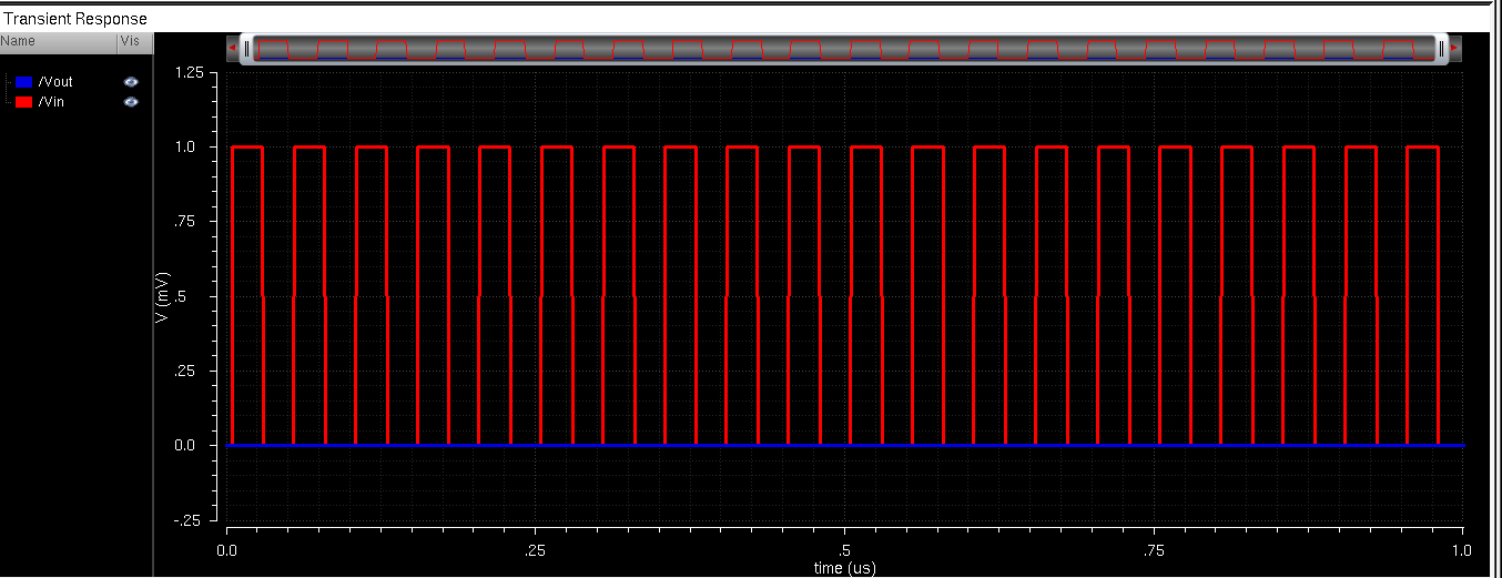
The least significant bit is determined by the formula (Reference Voltage)/(2^bits). In this case, that would be 5v/(2^10) = 4.9mV. I demonstrated this by running the simulation with a square wave that only had a 1mV amplitude. The results proved this to be true:
Main Lab
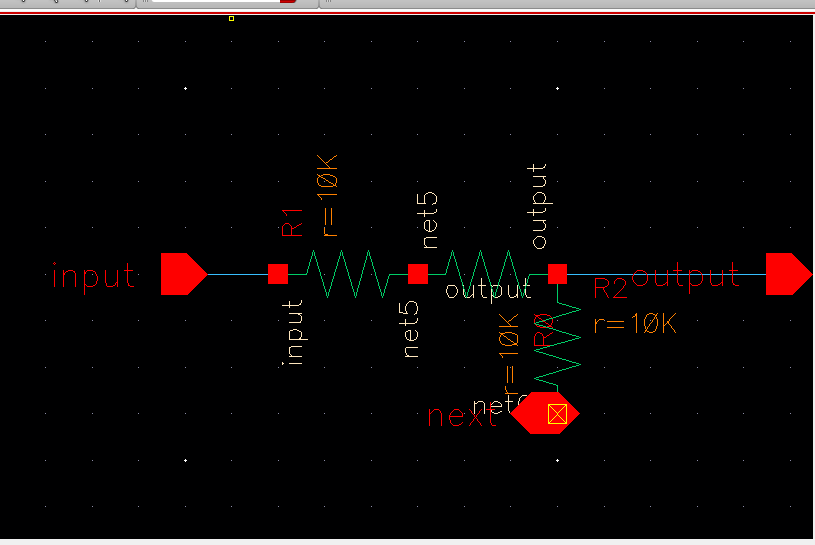
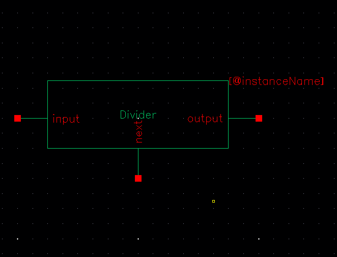
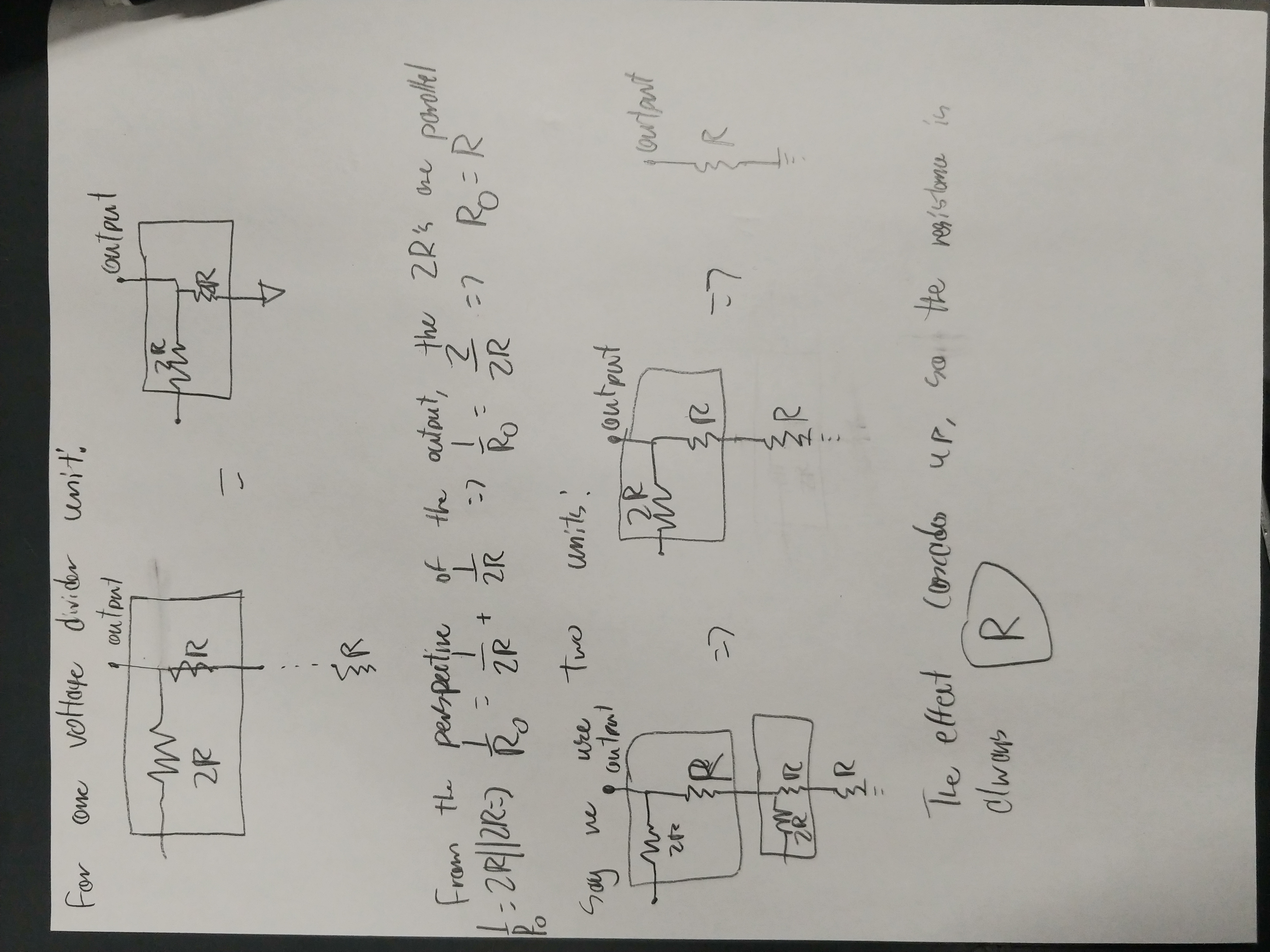
To create the DAC, I'll start by creating the individual switch/resistor units. Because of the presence of the ADC in the Prelab circuit, there is actually no need for the switches (the digital outputs of the ADC are effectively switches). Since the switches are unneccesary, I will only be making a voltage divider. I opened Cadence and created the following circuit diagram and then created its symbol:
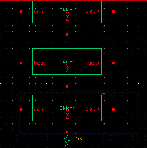
I then created the ADC by connecting the symbols in series, like so:
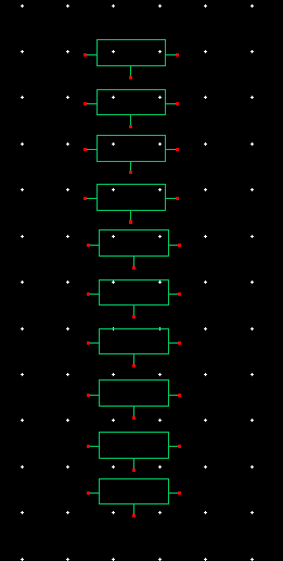
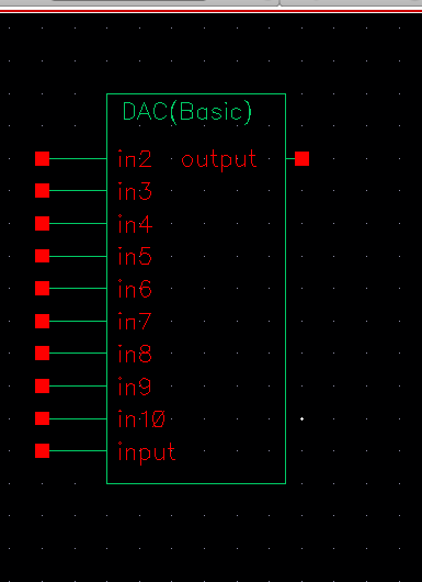
I converted it into a symbol and used the property editor to make sure it had the same footprint as the ideal ADC (height of 1.5, width of .6875):
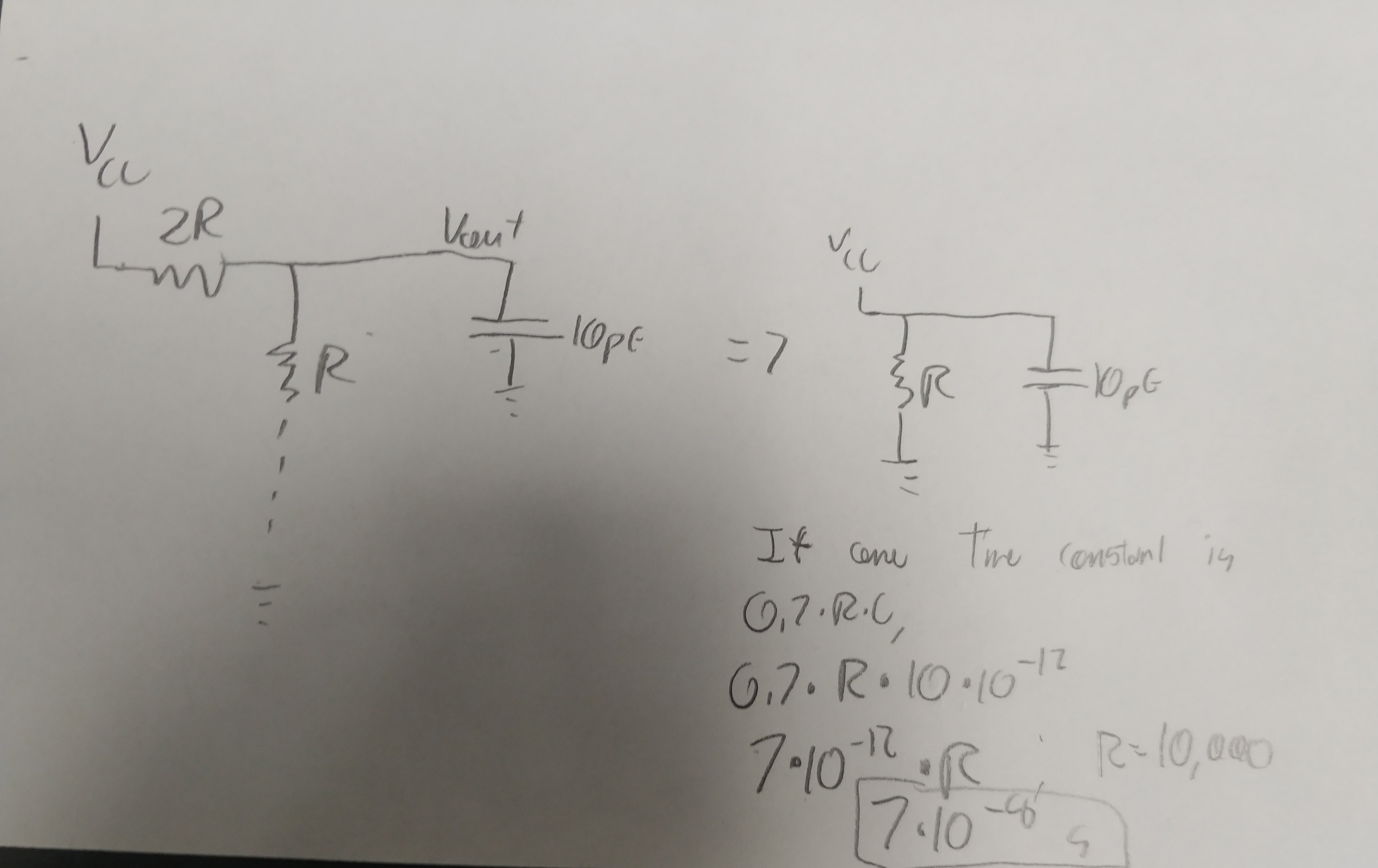
It is now ready for testing. To prepare for the tests, I did the necessary hand calculations first. They are shown below. The delay time I calculated was exactly 70 nanoseconds:
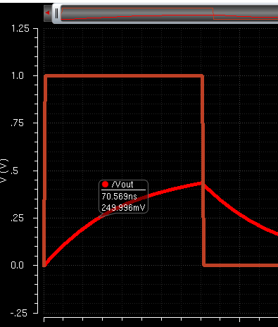
To test this, I created a circuit called "Tester", imported the DAC, and applied a voltage to it. I used a DC voltage at first to show that the steady state voltage was .5v (when 1 volt was applied). Then, I used a pulse to determine the delay of the circuit. The result was that it took 70 ns to reach .25v, which matches identically with the calculated values:
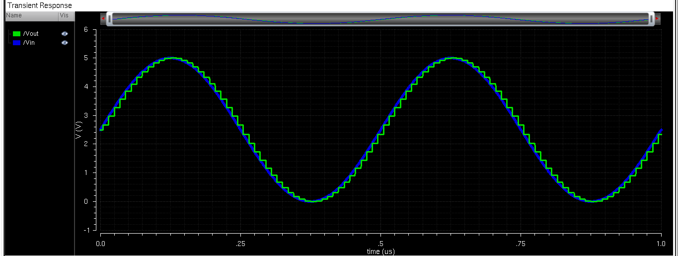
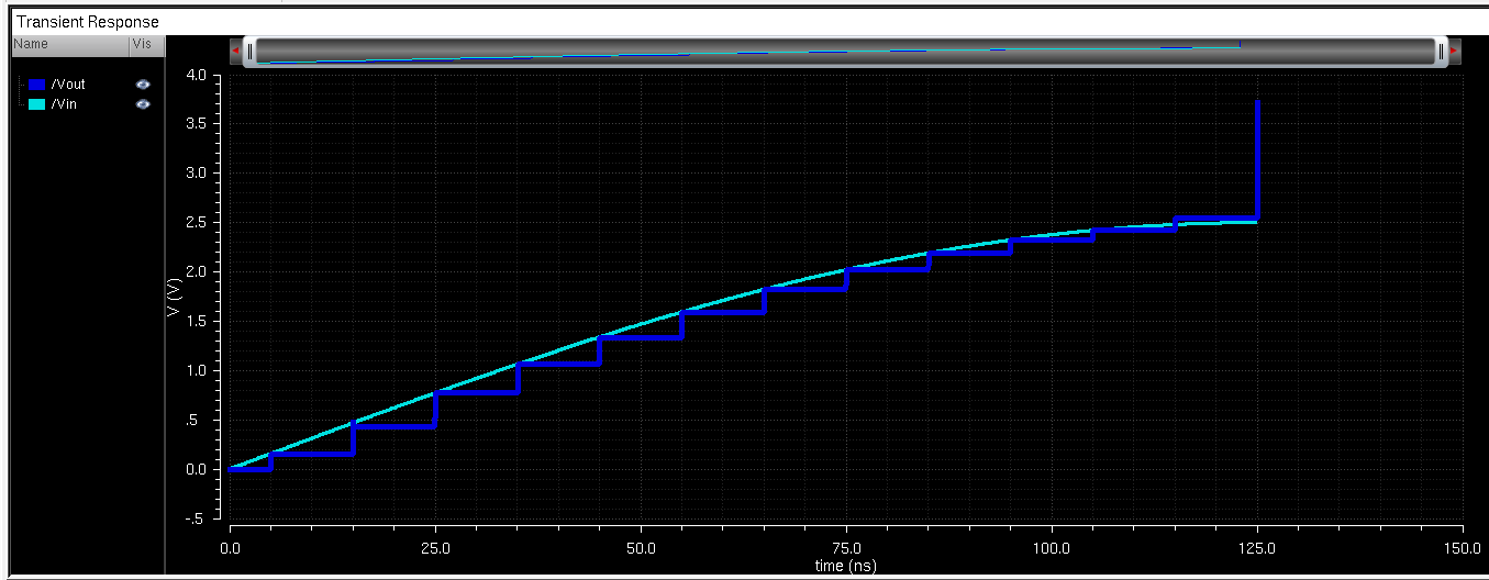
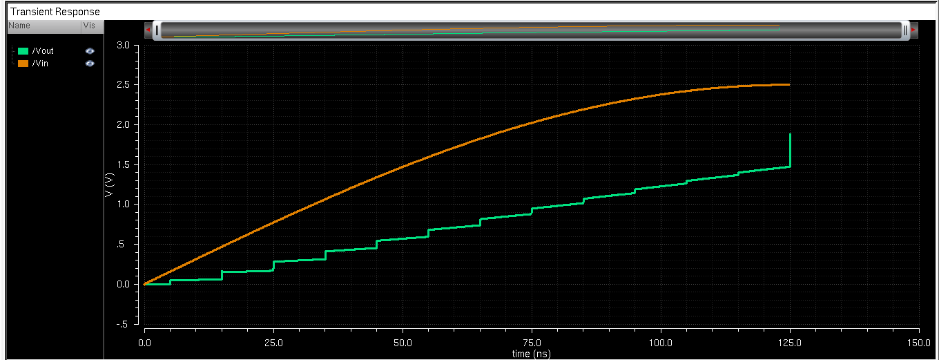
Next, I had to prove the design would work. I replaced the ideal ADC with my own and got the following simulation results:
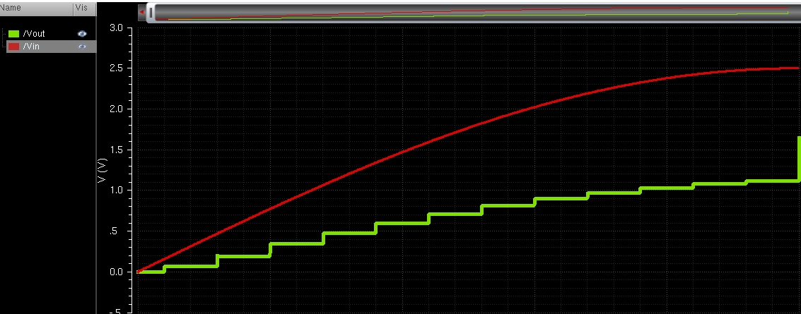
Under a 8k ohm resistive load, the output signal was scaled down:
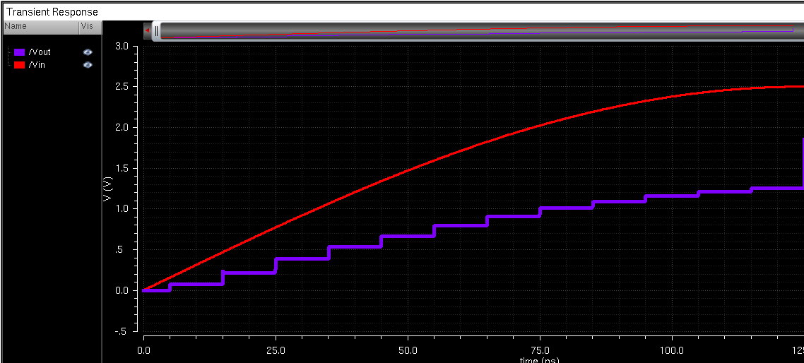
Under a 10k ohm resistive load, it was scaled similarly to the 8k resistive load. This is because, by Thevenin, the entire circuit can be made into a resistor and a voltage source. The scaling is a result of the Thevenin resistance of the circuit and voltage divider formed between the resistor and the circuit:
Under a strictly capacitive load of 10pF, it looked like this:
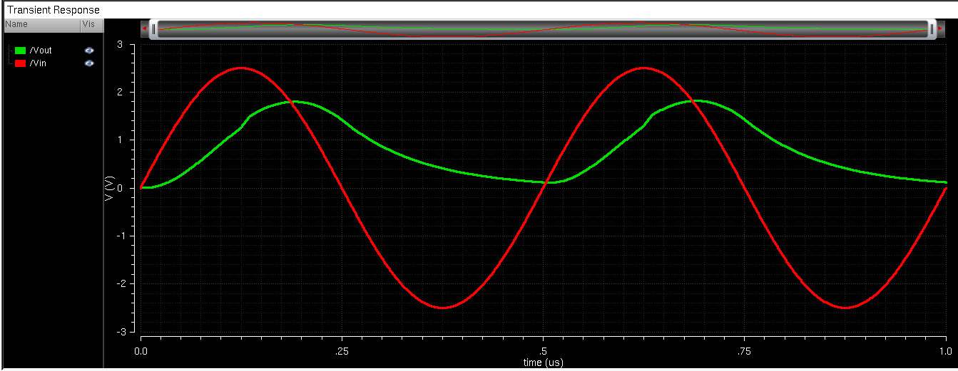
Under a resistive and capacitive load (10pF and 5k ohms), it looks like this:
Finally, let's assume the switches had a non-negligible resistance. We would simply have to factor that resistance into our calculation of the total resistance of the ADC (R). This would increase R.