Project - EE
421L
Email: boloor@unlv.nevada.edu
Project Guidelines:
Design, layout, and
simulate a digital receiver circuit that accepts a high-speed digital
input signal D and Di (a differential pair connected to your circuit from, for
example, a twisted pair of wires such as in an Ethernet cable). D and Di
are complements so, for example, if D is 5V then Di is 0V and output = 1.
Another example, when D is 1V and Di is 2V then output = 0. At high-speeds and
long distances the voltages received aren't full digital logic levels (i.e., 5V
and 0V), hence the need to design, and use, a high-speed digital
receiver circuit. Ideally, when D > Di the receiver outputs a 1. When D
< Di the receiver outputs a 0. Base your design on
the topology seen in Fig. 18.23. Try to design for high-speed and
low-power. Characterize your design (in sims) and the trade-offs. For
example, show that you get higher-speed if you use more energy (burn more
power). See if you can get, in this 500 nm process, 250 Mbits/s (a bit width of
4 ns) with an input voltage difference of, for example, 250 mV (with D and Di
swinging back and forth between 2.75V and 3V, for one of many examples,
your circuit outputs the correspondingly correct values). Note that while Fig.
18.23 shows one inverter on the output you may find, for
example, that two inverters work better (at the cost of power). Use a table
to summarize your design's performance.
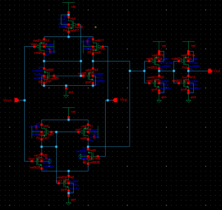
Design of Digital Receiver Circuit:
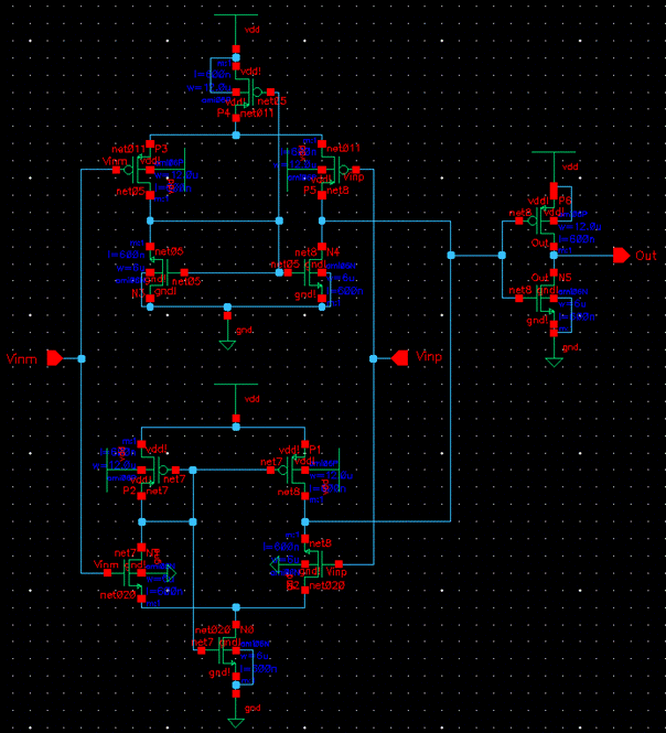
My initial design of the digital receiver
circuit is shown below. It follows the figure 18.23 topology. This circuit
uses an N flavor input buffer (bottom) in parallel with a P flavor input buffer
(top). Both input buffers use a self-biasing mechanism, which makes them
ideal for low power designs (as a biasing circuit is not necessary). Using the
two buffers in parallel has several benefits, such as better ensuring a full
GND-VDD voltage swing, decreasing the offset (seen when just the PMOS flavor is
used), and decreasing the propagation delays with low input voltages (seen when
just the NMOS flavor is used). The design uses the C5 process; all PMOS are
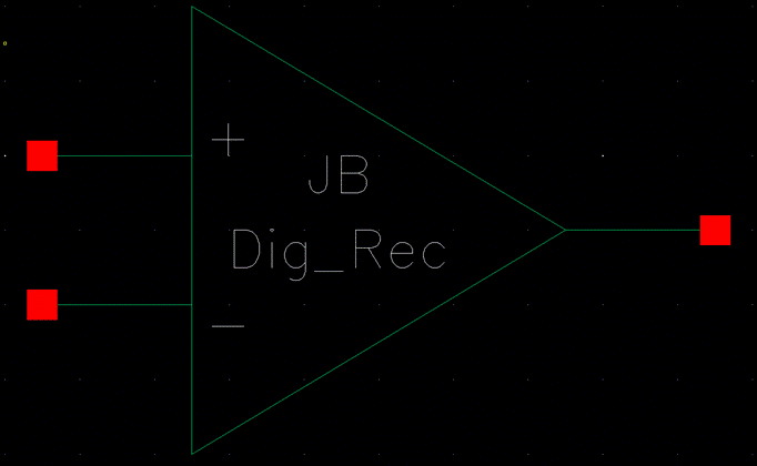
20/1 and all NMOS are 10/1. Alongside it is the symbol view created for it.
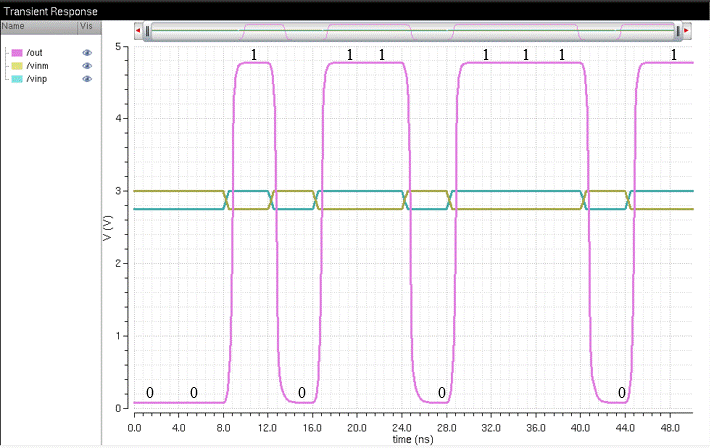
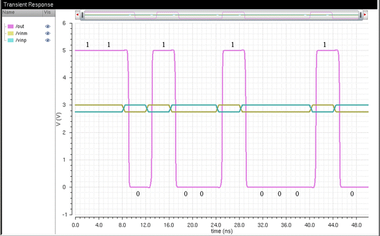
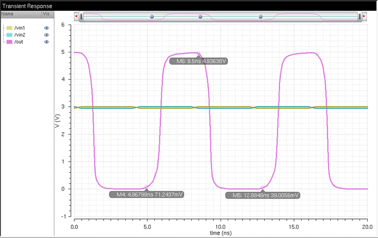
This circuit produced
the simulation results seen below when a random string of 1’s and 0’s was
inputted with a 250mV input voltage difference (Vinm = 1101 0010 0010, Vinp =
0010 1101 1101). The simulation shows that when Vinm is greater than Vinp, the
output goes low. When Vinm is less than Vinp, the output goes high. As the two
inputs are complements, the digital receiver is working as expected – the
output is 0010 1101 1101, following Vinp. Note that the output does not fully
reach VDD or GND, and there is a noticeable delay when the output switches.
These are the things I wanted to change.
Tradeoffs Considered
with the Final Design:
The initial simulation
above is not very clean, which prompted me to add another inverter with 10/1
device sizes to the design. Additionally, I reduced the widths of the PMOS
devices in the buffers to 6u, as it did not noticeably change the results. Decreasing
the width of devices lowers layout size and power consumption, but also limits
the speed that current can pass through.
This circuit was to be
designed for high speed and low power. The additional inverter mentioned above
obviously came at the cost of power consumption, but it was necessary for good
operation (a third inverter would slightly improve the results as well but was
not included because of the additional power it would consume). To decrease the
power consumption, I also modified the bottom NMOS
and top PMOS seen in the original design by increasing their lengths from 0.6u
(minimum) to 2.4u. Increasing the lengths of the tail MOSFETS make the
overall power consumption go down, as the circuit cannot run as fast
(hence, the speed of the design was slightly slower). This happens because
current has a longer path to conduct through when a minimum length device is
not used. Nonetheless, the design of the circuit after these changes both fit
the guidelines of the project and my liking.
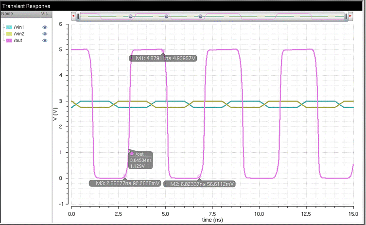
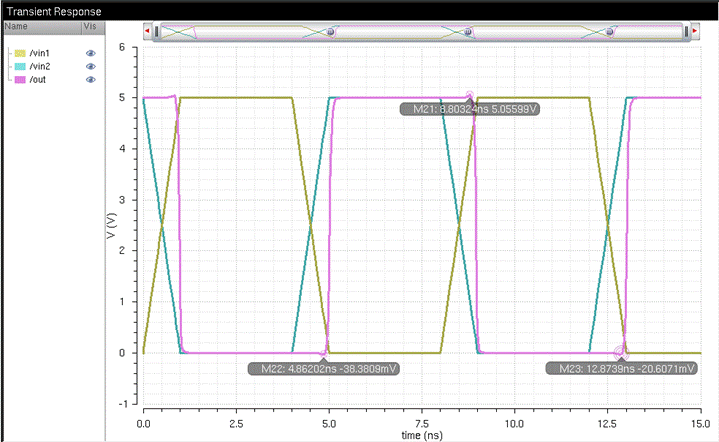
The final design of my
project is shown below, followed by its output when Vinm and Vinp are fed the same
random string of 1’s and 0’s as above with a 250mV difference. Clearly, this
device operates better.
It should be noted that
because only one additional inverter is used, the polarity of the output is
flipped.
The bit width is
4ns, separated clearly on the time axis. Vinm = 1101 0010 0010, Vinp = 0010
1101 1101. The output is indicated on the figure (1101 0010 0010), it
follows Vinm, as expected (because polarity is flipped).
Power Comparisons
To find out how much
power the circuit needed to be supplied, the following equation can be
used:
![]()
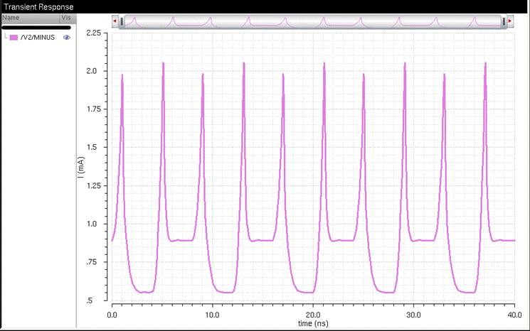
To find the average
current through the power supply, I plotted the current through the VDD source
and took its average. Note that when I did this, I used inputs with 8 ns
periods and clipped the current from 24 ns to 32ns, as the current was the
circuit starts up is much higher than its average for the rest of its
operation. The images below show the average current plot and calculation when
the input voltages swing between 2.75 and 3 volts.
|
|
|
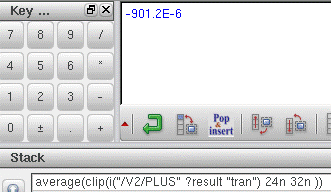
Using this number in the
average power equation, we have:
![]()
![]()
![]()
I repeated this process
several times with different input voltages. The table below summarizes the
average current and power supplied to the digital receiver by the power source.
Again, one of the major tradeoffs to consider in this design involved power and
speed. The power that was saved with changes in the original design is
depicted. This (around half) decrease in power came at the cost of a slightly
slower speed, but the device still operated well beyond the project guidelines.
|
Input Voltages |
Difference in Input
Voltage |
Average Power Supplied
to Original Design |
Average Power Supplied
to My Design |
Average Current Pulled
from VDD in My Design |
|
3 V and 2.85 V |
150 mV |
9.67 mW |
5.37 mW |
1.073 mA |
|
3 V and 2.75 V |
250 mV |
8.79 mW |
4.51 mW |
901.2 µA |
|
1 V and 1.5 V |
500 mV |
7.59
mW |
3.45
mW |
689.3
µA |
|
1 V and 2 V |
1 V |
6.87 mW |
2.99 mW |
598.2 µA |
|
2 V and 4 V |
2 V |
6.26 mW |
2.86 mW |
572.8 µA |
|
2 V and 5 V |
3 V |
6.02 mW |
2.79 mW |
558.2 µA |
|
0 V and 4 V |
4 V |
5.09 mW |
2.27 mW |
453.1 µA |
|
0 V and 5 V |
5 V |
4.91 mW |
2.23 mW |
446.6 µA |
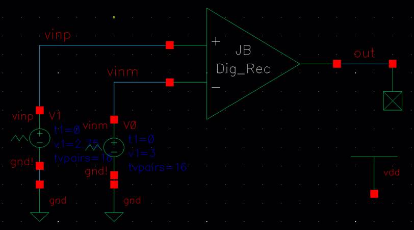
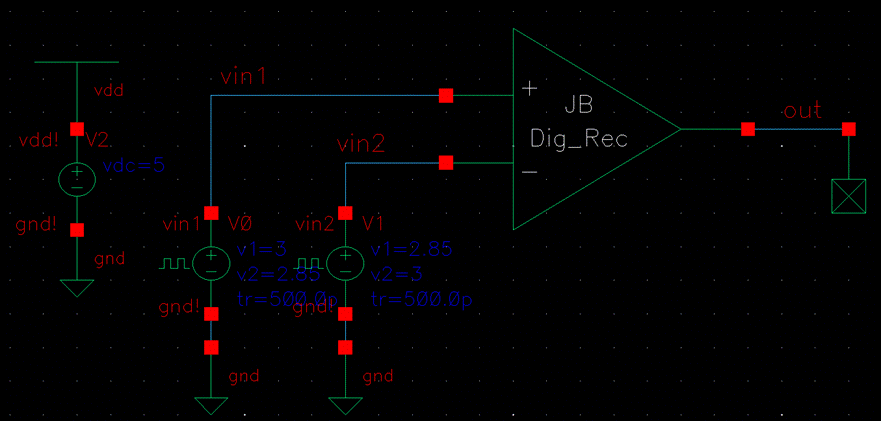
Simulating the Digital Receiver Circuit:
The following section of
this report will further characterize and test the design through simulations.
These simulations show the circuit working under a variety of test conditions.
All use a variation of the following schematic:
Input Voltage and Bit
Width Effects:
The following table
shows the performance of the design under different input voltages and bit
widths.
|
Parameters Being Tested / Additional Notes |
Simulation |
|
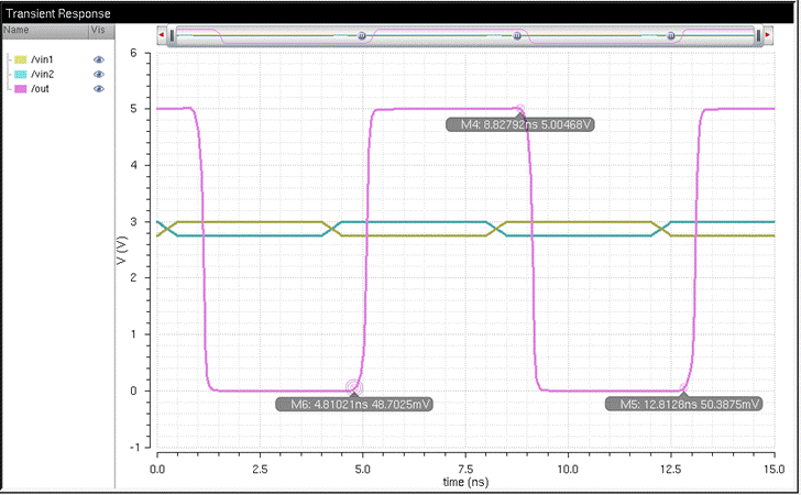
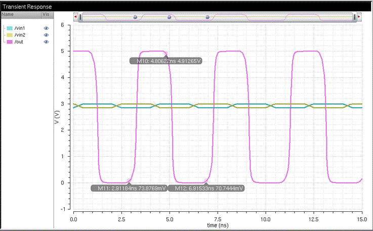
·
250 Mbits/s (a bit width of 4 ns) with an input voltage
difference of 250 mV. ·
Rise/Fall time = 500ps The circuit can
operate under these conditions. |
|
|
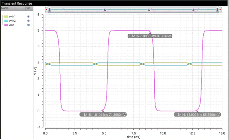
·
250 Mbits/s (a bit width of 4 ns) with an input voltage
difference of 150mV ·
Rise/Fall time = 500ps The circuit can
operate under these conditions. |
|
|
·
250 Mbits/s (a bit width of 4 ns) with an input voltage
difference of 100mV ·
Rise/Fall time = 500ps The circuit can
operate under these conditions, but accuracy begins to deteriorate very slightly. |
|
|
·
250 Mbits/s (a bit width of 4 ns) with an input voltage
difference of 50mV ·
Rise/Fall time = 500ps The circuit precision
deteriorates under these conditions. Therefore, accuracy at 250 Mbits/s
with an input voltage difference smaller than 50 mV will begin to worsen. |
|
|
·
500 Mbits/s (a bit width of 2 ns) with an input voltage
difference of 250 mV ·
Rise/Fall time = 500ps The circuit can
operate under these conditions. |
|
|
·
500 Mbits/s (a bit width of 2 ns) with an input voltage
difference of 150 mV ·
Rise/Fall time = 500ps The circuit can
operate under these conditions, but accuracy begins to deteriorate slightly.
Therefore, accuracy at 500 Mbits/s with an input voltage difference
smaller than 150 mV will begin to worsen. |
|
|
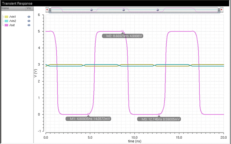
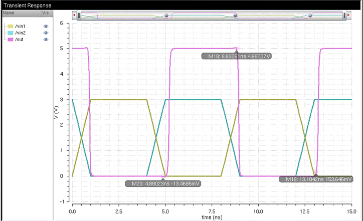
·
250 Mbits/s (a bit width of 4 ns) with an input voltage
difference of 3 V ·
Rise/Fall time = 1ns The circuit can
operate under these conditions. |
|
|
·
250 Mbits/s (a bit width of 4 ns) with an input voltage
difference of 5 V ·
Rise/Fall time = 1ns The circuit can
operate under these conditions. |
|
These simulations prove
that the device works well past the design guidelines for both bit width and
input voltage difference.
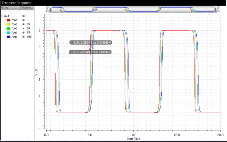
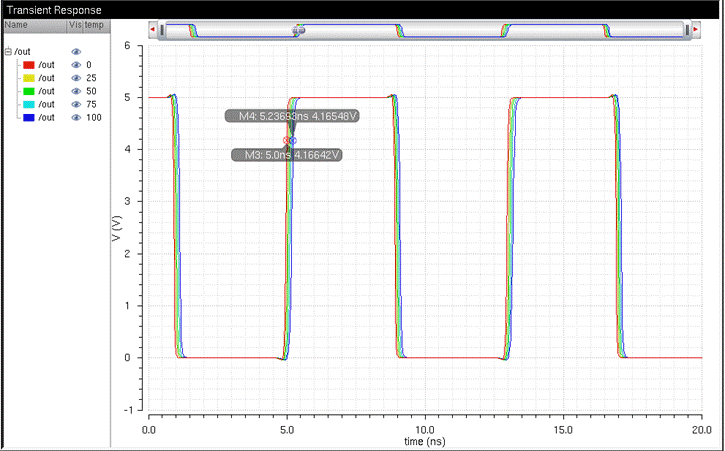
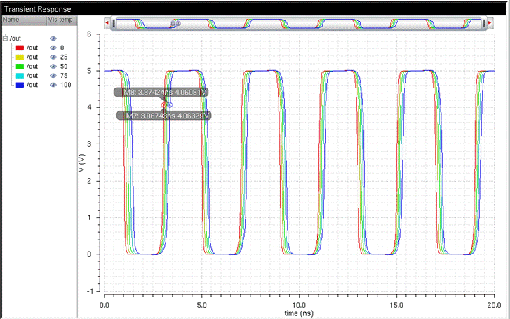
Temperature Effects:
To show the way the
circuit operates with changes in temperature, a parametric analysis of the
output can be simulated. A benefit to using this topology for the rail to rail
input buffer is that it is resistant to changes in temperature. This holds
mostly true for my design. I swept the temperature from 0 to 100˚C and
provided the output simulations for a few different inputs. All show relatively
small variations in output.
|
Parameters Being
Tested / Additional Notes |
Temperature Sweep Simulation |
|
·
250 Mbits/s (a bit width of 4 ns) with an input voltage
difference of 250 mV. ·
Rise/Fall time = 500ps Around 5 mV change in
voltage over 100˚ |
|
|
·
250 Mbits/s (a bit width of 4 ns) with an input voltage
difference of 5V ·
Rise/Fall time = 1ns Around 1mV change in
voltage over 100˚ |
|
|
·
500 Mbits/s (a bit width of 2 ns) with an input voltage
difference of 250 mV ·
Rise/Fall time = 500ps Around 350 mV change
in voltage over 100˚. This simulation saw
the largest variation in output with change in temperature, which was to be
expected as it tested the smallest bit width. |
|
This concludes the
simulation section of the project report. The next section will show the layout
of the design.
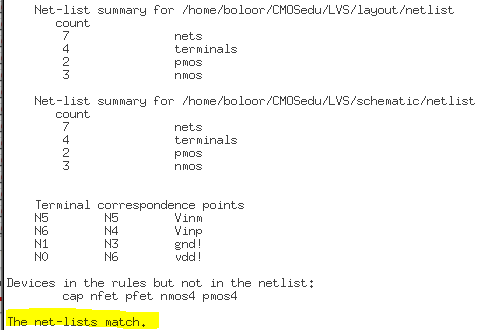
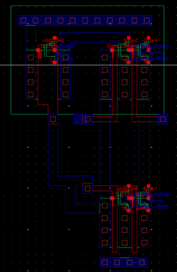
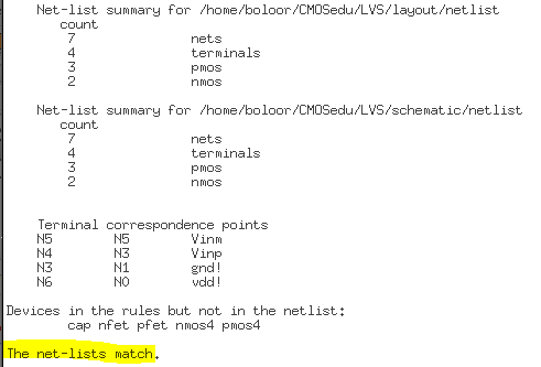
Digital Receiver Layout
The below images show
the pieces that I used in my digital receiver layout. Each was individually
laid out and verified. The last section shows my final layout.
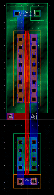
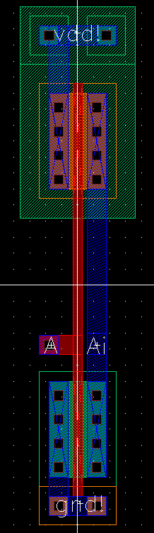
NMOS Flavor Input Buffer
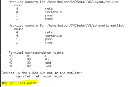
Layout, Extracted View, and DRC/LVS Verifications:
|
|
|
PMOS Flavor Input Buffer
Layout, Extracted View, and DRC/LVS Verifications:
|
|
|
12u/6u (Left) and 6u/6u
(Right) Inverters Layout, Extracted View, and DRC/LVS Verifications:
|
|
|
|
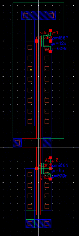
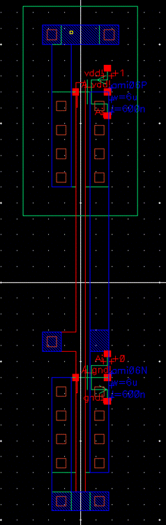
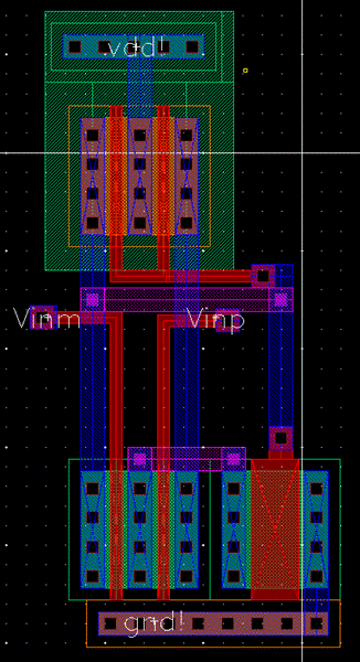
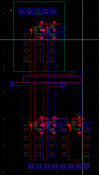
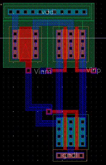
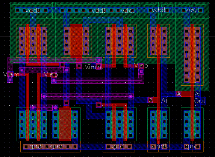
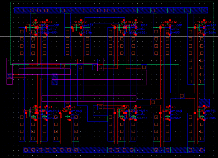
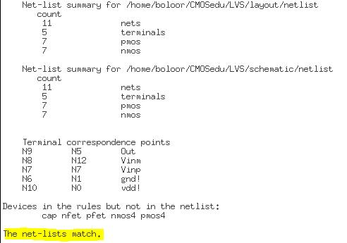
Final Rail to Rail Input
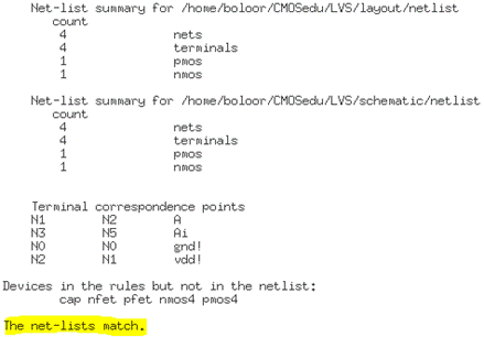
Buffer Layout, Extracted View, and DRC/LVS Verifications:
|
|
|
|
|
|
Zipped up directory of the
project: 421 Lab Project Zip
The last step I took in
completing this lab was backing up all my work to my Google Drive. This
concludes the lab work.