Email: boloor@unlv.nevada.edu, morenc6@unlv.nevada.edu
Prelab:
- Back-up
all of your work from the lab and the course.
- Go
through Cadence Tutorial 6 seen here.
- Read
through the lab in its entirety before starting to work on it
Tutorial 6 called for us to layout a chip for fabrication.
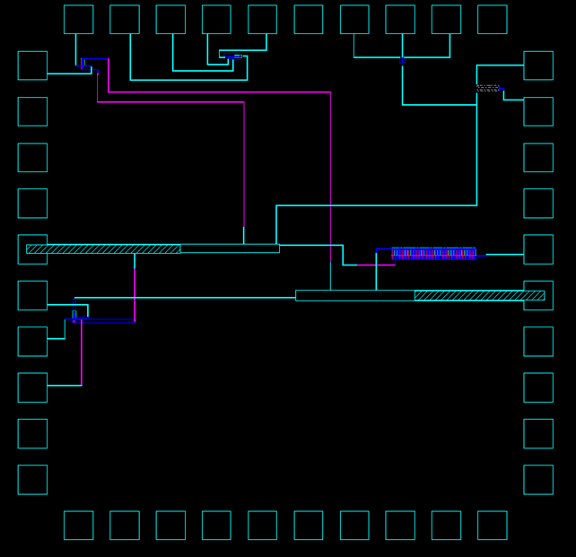
The first step in this process is laying out and verifying a pad
frame. The bonding diagram and layout is showing below:
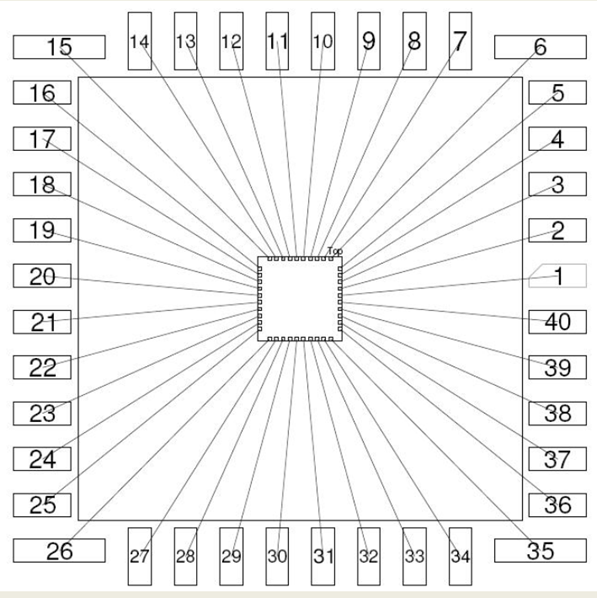
The layout passed
both DRC and LVS verifications.
Next, we were to
place several circuits and devices into the pad frame. The prelab called for:
·
NMOS and PMOS
·
31 stage Oscillator
·
Voltage divider
·
Inverter
·
NAND
·
GND and VDD
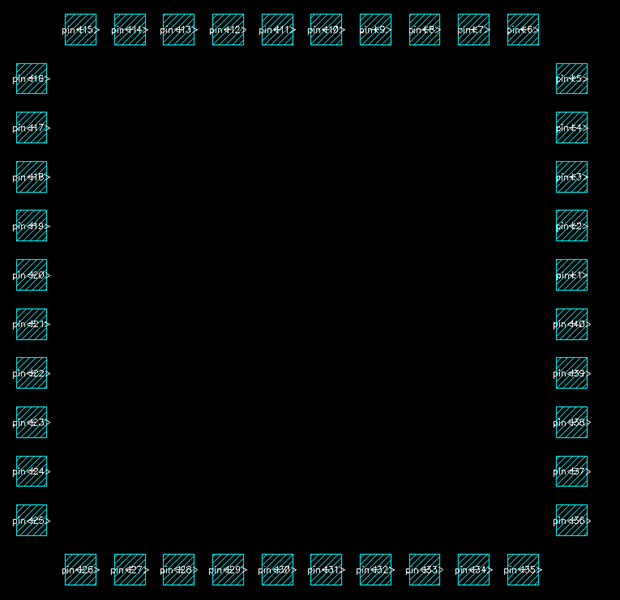
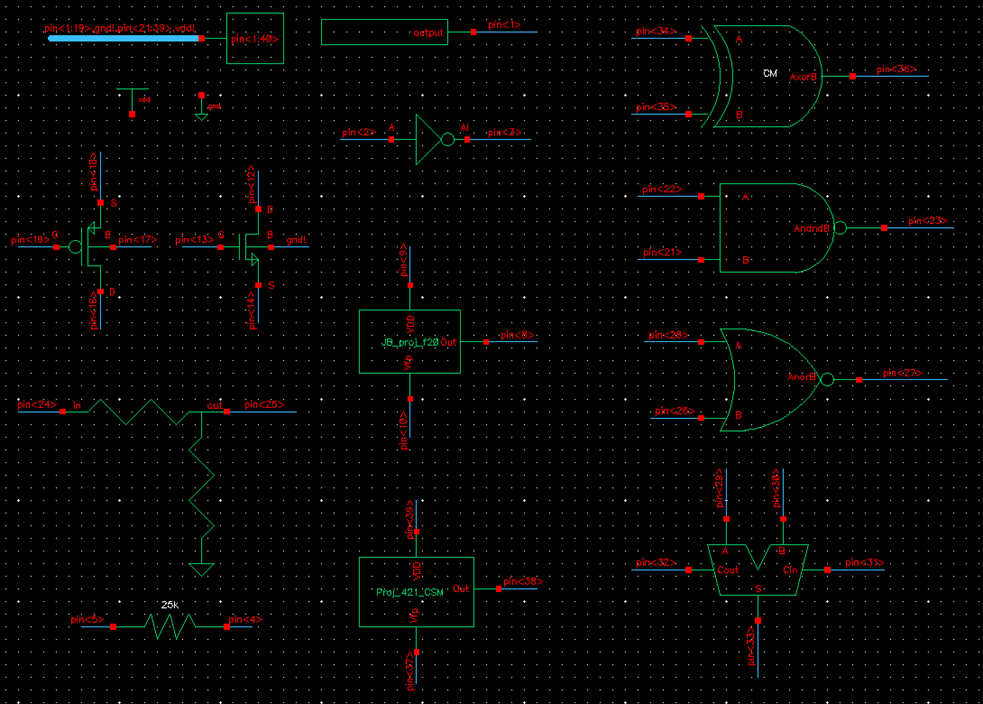
The image below shows
all of the symbol views for these components on the
schematic. This is what the chip will lay out.
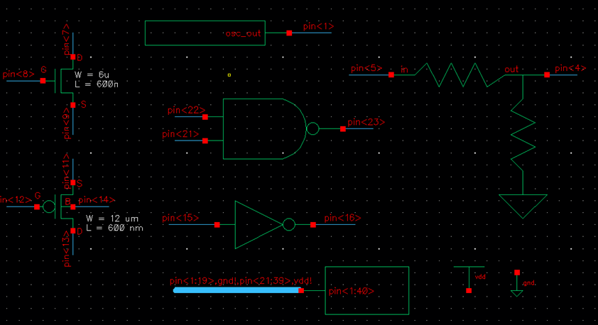
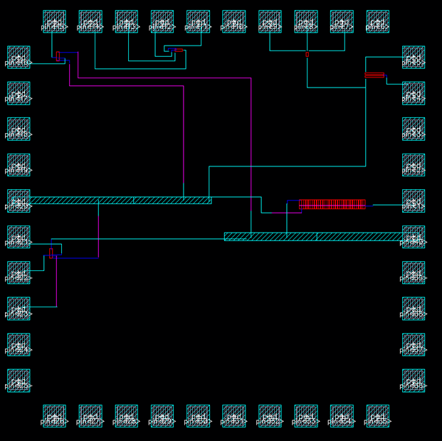
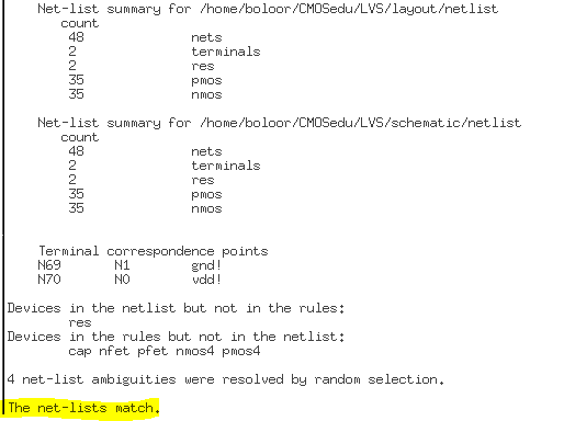
The circuits were
laid out, connected to pads and verified. The final
layout with its extracted view is shown below.
LVS and DRC verifications for the above
schematic/layout:
![]()
Lastly, I backed up my work to my
Google Drive. This concludes the work for the prelab.
Lab Work: Generate a
test chip layout for submission to MOSIS for fabrication.
Your chip should include
the following test structures:
- One, or more if possible,
course projects
- A 31-stage ring oscillator with
a buffer for driving a 20 pF off-chip load
- NAND and NOR gates using 6/0.6
NMOSs and PMOSs
- An inverter made with a 6/0.6
NMOS and a 12/0.6 PMOS
- Transistors, both PMOS and
NMOS, measuring 6u/0.6u where all 4 terminals of each device are connected
to bond pads (7 pads + common gnd pad)
- Note that only one pad is
needed for the common gnd pad. This pad is used
to ground the p-substrate and provide ground to each test circuit
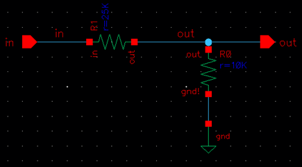
- Using the 25k resistor laid out
below and a 10k resistor implement a voltage divider (need only 1 more pad
above the ones used for the 25k resistor)
- A 25k resistor implemented
using the n-well (connect between 2
pads but we also need a common gnd pad)
- Whatever else you would like to
fabricate to use the remaining pins on the chip
Team Member Responsibilities:
·
Cole: Layout of NMOS, PMOS, Divider,
XOR, NOR, Inverter, Dull Adder
·
Jazmine: Layout of 31-stage ring
oscillator with buffer, writing report
Our test chip was
named Chip2_f20. A zipped directory of our design can be downloaded here.
In addition to all of the required test structures, and also included a full
adder and both of our course projects (switching power supply controller chip
for a flyback SPS) to the chip. The following section of this report
illustrates the design details of each of the required test structures.
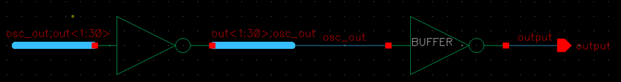
31-Stage Ring
Oscillator with Buffer for Driving 20 pF Off-Chip Load:
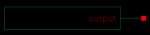
Schematic/Symbol/Layout:
Calculations for
Buffer to drive 20pF:
The input capacitance of one 12/6
inverter is 36fF, calculated below.
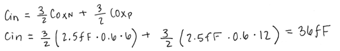
The following combination of inverters
allotted approximately 25pF of capacitance. This was suitable for the off-chip
capacitor, and was the design used.
Capacitance from inverter to inverter can be calculated as
![]()
A is the multiplicity factor
between lengths and widths of the devices. In this case, A = 4 between the
second and third device. The final capacitance is
![]()
![]()
![]()
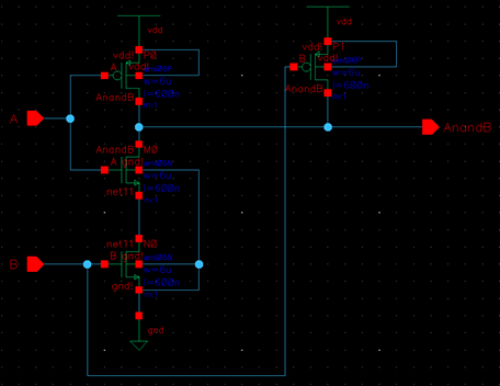
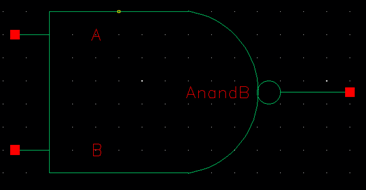
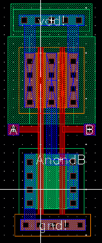
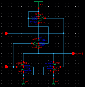
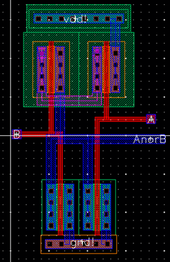
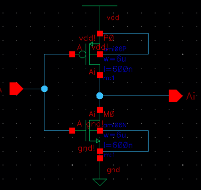
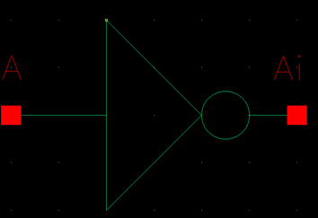
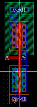
NAND and NOR Gates
using 6/0.6 NMOSs and PMOSs:
Schematic/Symbol for
NAND Gate:
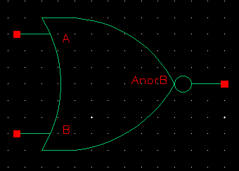
Schematic/Symbol/Layout
for NOR Gate:
Inverter Using 6/0.6
NMOS and 12/0.6 PMOS:
Schematic/Symbol/Layout:
NMOS and PMOS
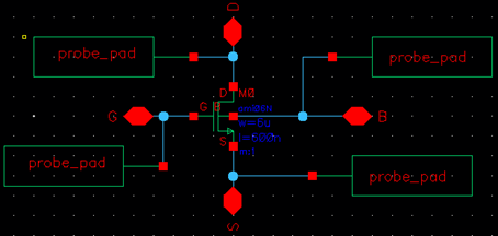
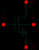
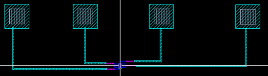
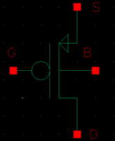
Measuring 6u/0.6u with bond pads:
NMOS
Schematic/Symbol/Layout:
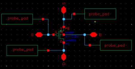
PMOS
Schematic/Symbol/Layout:
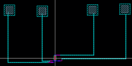
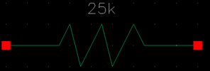
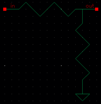
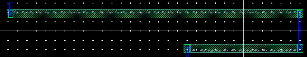
25k Resistor and
25k/10k Voltage Divider:
25k Resistor
Symbol/Layout:
![]()
25k/10k Voltage
Divider Schematic/Symbol/Layout:
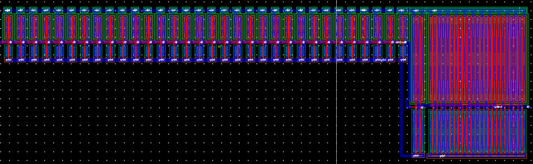
The Chip: This section of the report will
characterize the chip.
Schematic:
Layout:
Pin Diagram: The chip will be packaged in order to
test it. VDD (Pin 40) and GND (Pin 20) must be applied to test this chip.
|
Pin Number |
Description |
Testing Details |
|
Pin 1 |
Oscillator Output |
Oscillating output will be shown though this pin if probed. |
|
Pin 2 |
Inverter Input |
Connect off chip voltage to this pin. |
|
Pin 3 |
Inverter Output |
Voltage applied to pin 2 will be inverted. |
|
Pin 4 |
Resistor input |
Connect off chip voltage to this pin. |
|
Pin 5 |
Resistor output |
Output of resistor will show on this pin. |
|
Pin 6 |
No Connection |
|
|
Pin 7 |
No Connection |
|
|
Pin 8 |
Jazmine’s SPS Output |
Switching power supply output |
|
Pin 9 |
Jazmine’s SPS VDD |
Connect 5V DC source |
|
Pin 10 |
Jazmine’s SPS Vfp |
Connect off chip voltage to this pin. Hysteresis is acceptable. |
|
Pin 11 |
No Connection |
|
|
Pin 12 |
NMOS Drain |
Connect off chip voltage to this pin. |
|
Pin 13 |
NMOS Gate |
Connect off chip voltage to this pin. |
|
Pin 14 |
NMOS Source |
Connect off chip voltage to this pin. |
|
Pin 15 |
No Connection |
|
|
Pin 16 |
PMOS Drain |
Connect off chip voltage to this pin. |
|
Pin 17 |
PMOS Body |
Connect off chip voltage to this pin. |
|
Pin 18 |
PMOS Source |
Connect off chip voltage to this pin (same as pin 18 to
eliminate body effect). |
|
Pin 19 |
PMOS Gate |
Connect off chip voltage to this pin |
|
Pin 20 |
GND |
GND for entire chip. Must be connected to a ground source for
proper chip operation. |
|
Pin 21 |
NAND Gate A |
Connect off chip voltage to this pin. |
|
Pin 22 |
NAND Gate B |
Connect off chip voltage to this pin. |
|
Pin 23 |
NAND Gate Output |
A NAND B (Pin 21 NAND Pin 22) will be outputted through this
pin. |
|
Pin 24 |
Voltage Divider Input |
Connect off chip voltage to this pin. |
|
Pin 25 |
Voltage Divider Output |
Half of voltage applied to pin 24 will be outputted through this
pin. |
|
Pin 26 |
NOR Gate A |
Connect off chip voltage to this pin. |
|
Pin 27 |
NOR Gate B |
Connect off chip voltage to this pin. |
|
Pin 28 |
NOR Gate Output |
A NOR B (Pin 34 NOR Pin 35) will be outputted through this pin. |
|
Pin 29 |
Full Adder A |
Connect off chip voltage to this pin. |
|
Pin 30 |
Fuller Adder B |
Connect off chip voltage to this pin. |
|
Pin 31 |
Full Adder Cin |
Connect off chip voltage to this pin. |
|
Pin 32 |
Full Adder Cout |
Connect off chip voltage to this pin. |
|
Pin 33 |
Full Adder Sum |
Sum of full adder will be outputted through this pin. |
|
Pin 34 |
XOR Gate A |
Connect off chip voltage to this pin. |
|
Pin 35 |
XOR Gate B |
Connect off chip voltage to this pin. |
|
Pin 36 |
XOR Gate Output |
A XOR B (Pin 34 XOR Pin 35) will be outputted through this pin. |
|
Pin 37 |
Cole’s SPS Vfp |
Connect off chip voltage to this pin. Hysteresis is acceptable. |
|
Pin 38 |
Cole’s SPS Output |
Switching power supply output |
|
Pin 39 |
Cole’s SPS VDD |
Connect 5V DC source |
|
Pin 40 |
VDD |
VDD for entire chip. Must be connected to a 5V reference source
for proper chip operation. |
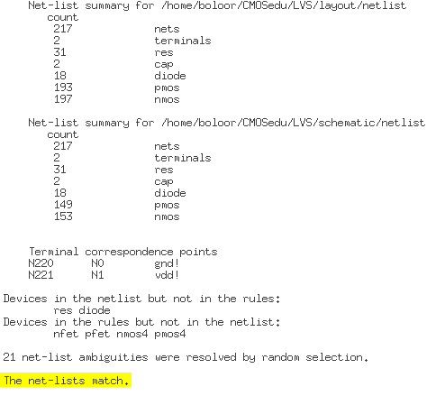
DRC/LVS
Verifications:
![]()
The last step we took in our lab
work was backing up our work to Google Drive.