Lab 3 - EE
421L
Email: boloor@unlv.nevada.edu
Prelab: Backup all
previous work and complete tutorial one.
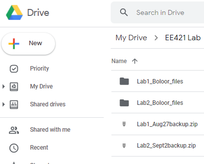
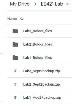
My previous lab work has been backed up to my Google Drive, as
shown below.
The remainder of tutorial one walks
through the process of making a resistor and a resistive divider in Cadence.
The following image shows the extracted view of a 10.21k resistor.

The value of the resistor can clearly
be seen with the orange font in the extracted view.
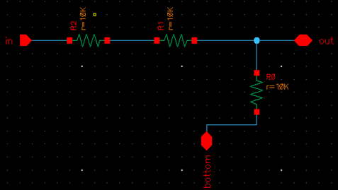
Next, the tutorial goes through how to make a resistive divider.
The resistor shown above was instantiated twice and connected through metal
layer 1.
The design passed the LVS verification, meaning the layout and
schematic match.

Lab Work:
- Use the n-well to layout a 10k
resistor as discussed in Tutorial 1
- Discuss, in
your lab report, how to select the width and length of the resistor by
referencing the process information from MOSIS
- Use this n-well resistor in the
layout of your DAC
- Discuss, in
your lab report, how the width and length of the resistor are
measured
- Ensure that each resistor in
the DAC is laid out in parallel having the same x-position but varying
y-positions (the resistors are stacked)
- All input and output Pins
should be on metal 1
- DRC and LVS, with the extracted
layout, your design (show the results in your lab report)
- Zip up your final design
directory and place it in the lab3 directory, with a link on your lab
report, so the grader can examine both the layout and schematic (and
simulations)
·
Ensure that your html
lab report includes your name and email address at the beginning of the report
(the top of the webpage).
·
When finished backup your
work (webpages and design directory).
Picking a Length and Width:
To create the 10k resistor with the C5
process, the MOSIS parameters file has the information needed to select a
length and width. The file lists that the sheet resistance of the n-well
used in the design is about 800 Ohms. The minimum width is 12 lambda (lambda =
0.30um), so the minimum width is 3.6 microns. Using this minimum value and the
desired resistance of 10k, the following equation can be used to calculate the
desired length:

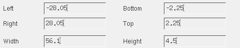
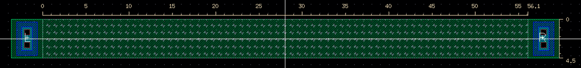
So, the desired length is around 45 microns, and the minimum width
is 3.6 microns. For the sake of the tutorial, I used a length of 56.1 um and a
width of 4.5 um.
Measuring the Length and Width of the Resistor:
A ruler can be created by using the Bindkey k (or Tools
> Create Ruler). Click to begin and end a measurement.
Laying Out the DAC:
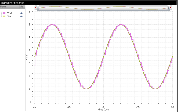
The following images were taken from my Lab 2, and they show the
schematic and simulation of the DAC I made under no load conditions. It shows
to work properly.
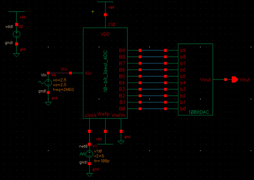
The next images, also
taken from lab 2, show the schematic that I was following for my layout (and
that I used in the LVS verification). The image on the left shows the contents
of each of the square symbols in the image on the right. Therefore, thirty-one
10k resistors are needed for this design.
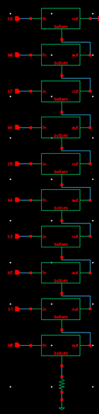
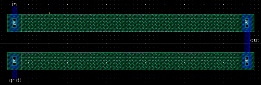
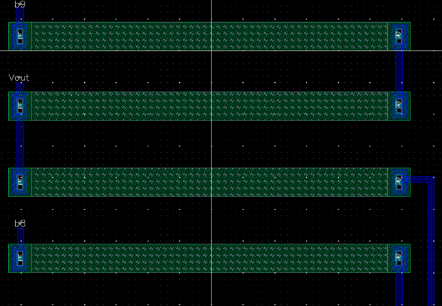
To make the layout for this schematic, I instantiated thirty-one
10k resistors. As mentioned in tutorial 1, the resistors could not be too close
to each other because it would cause a design error. Each resistor is laid
out in parallel with the same x-position, but varying y-positions. The
resistors are connected through metal1, and all of the input and output pins
are also on this layer. Below is a screenshot of the full design, as well
as a few close-up views of the stacked resistors.
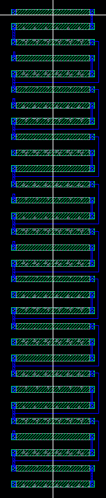
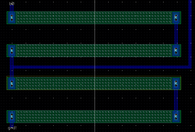
Full View View
of top View
of bottom
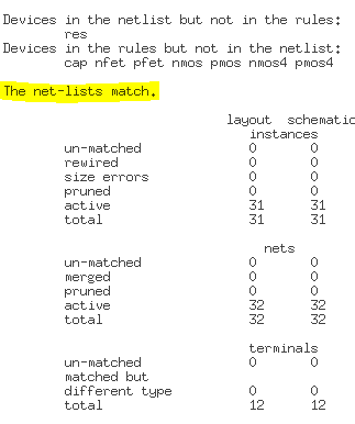
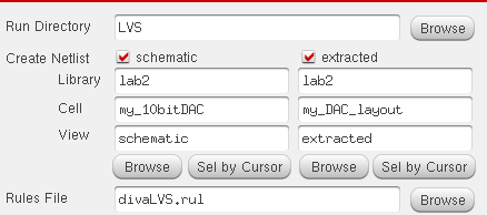
Verification Results:
The design passed the DRC check (after
making minor adjustments to snap the design to the grid), and then passed the
LVS verification – the netlists match.
![]()
Backing Up Work:
The last step I took in completing
this lab was backing up my work to my Google Drive the same way I did in the
prelab and in the labs prior.
This concludes lab 3.