Lab 2 - EE
421L
Author: Jazmine Boloor,
Email:
boloor@unlv.nevada.edu
Due Date: September 9
Prelab:
·
Prior to coming to lab make sure you understand
how the input voltage, Vin, is related to B[9:0] and Vout
Answer: The input voltage, Vin, is related to B[9:0]
as this is the binary representation of it in ten bits (bits 0 to 9) when
outputted from the ADC. These bits are then inputted into the DAC, which
outputs an amplitude based on its input. So, the larger the input bit (from
0-9), the larger the amplitude of Vout. As the DAC
analyzes each bit in time, it outputs a constant height which accounts for the
square waveform shown in the lab simulations. This constant amplitude is the
analog value of the signal.
- In your lab report: 1) provide narrative of the steps
used, 2) provide, and discuss, simulation results different from the above
to illustrate your understanding of the ADC and DAC, 3) explain how you
determine the least significant bit (LSB, the minimum voltage
change on the ADC's input to see a change in the digital code B[9:0])
of the converter. Use simulations to support your understanding.
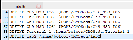
1) To begin this prelab,
I first added the command line highlighted below into my cds.lib folder.
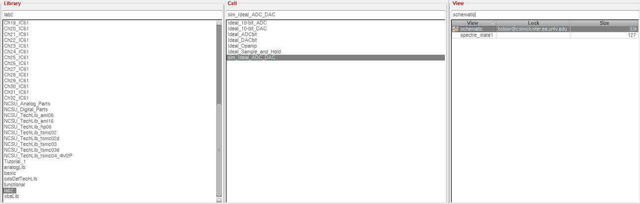
After adding this, I opened the following schematic shown in the
Library manager:
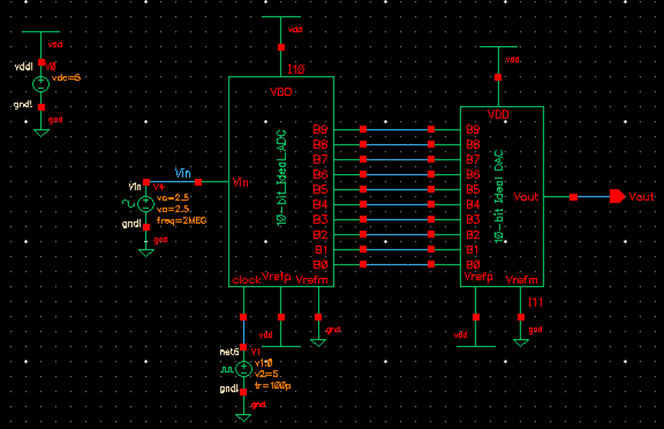
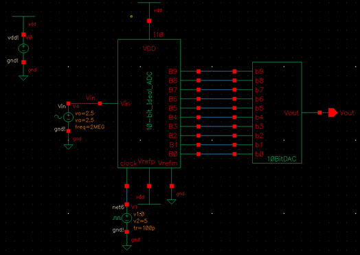
This opened the schematic shown on the left. The snip on the right
is the immediate waveform that is given after the ADE is launched, the state is
loaded, and the green start button is clicked.
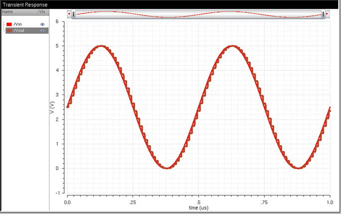
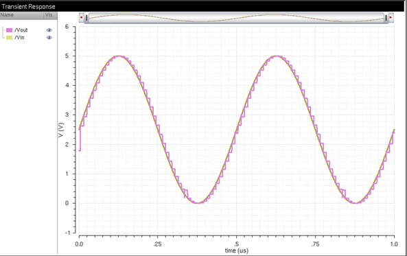
To make the waveform easier to see, I made the traces solid and thick. I
also changed the waveform background to white. The output has the square
pattern that is expected from a DAC – the amplitude of at each point on the
analog input signal corresponds to a digital amplitude value that is shown by Vout.
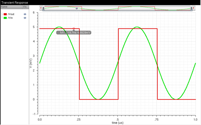
2) To further explain
how the DAC works, I changed the input voltage and offset to 5mV. The waveform
below shows how doing so will result in a considerably smaller number of
“steps” in the output when compared to the 2.5V input. This is due to the
considerably smaller amplitude change in the input. The way the DAC calculates
the height at which it steps is through the LSB, discussed in the next step.
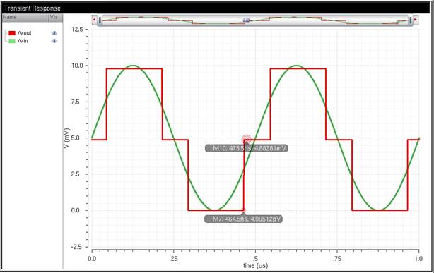
3) To calculate the least significant bit, I changed the input and
offset of the sine wave to 2.5mV (which I estimated using the LSB formula shown
in the next step). The bottom marker is approximately at zero volts, and the
first step occurs at approximately 4.88mV, marked on the waveform. Therefore,
4.88mV is the least significant bit, which is defined as the minimum change in
input to see a change in output.
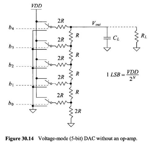
The equation shown in
figure 30.14 below can also be used to calculate the least significant bit: ![]() , where N is the number
of bits (bit 0 to bit 9 make a total of 10 bits), and VDD is our input voltage,
shown as 5V.
, where N is the number
of bits (bit 0 to bit 9 make a total of 10 bits), and VDD is our input voltage,
shown as 5V.
For the last step in the
prelab, I created a backup for the work I did.
___________________________________________________________________________________________________________________________________________________________________________________________________________________
Lab Work: In this lab
we will use n-well resistors to implement a 10-bit DAC.
The design is based upon the topology seen in
Fig. 30.14, below, in the CMOS book.
The controlling input bits seen below come from the ADC, in
other words the inputs to the DAC are the left side of the 2R resistors.
The resistance of the DAC can be found simply
by combining parallel and series resistors. The DAC follows a pattern
continuously creating two resistors in parallel with the same value and then
adding a resistor in series, eventually creating an Req = R. The following
image (based on Figure 30.14) shows the main idea of this method pictorially –
this pattern is followed all the way up the DAC.
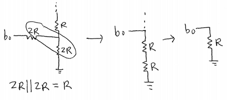
Therefore, the equivalent resistance of the DAC after combining
resistors in this manner for 10 bits is R.
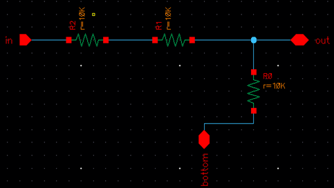
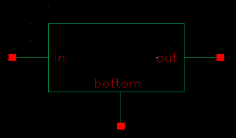
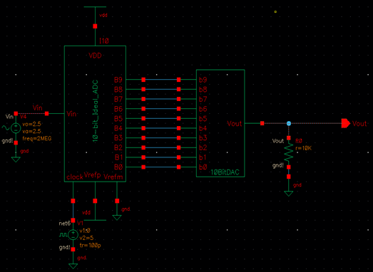
The first step that I took in building the 10-bit DAC in Cadence
was creating a symbol for circuitry seen at each bit input – two parallel
resistors in series with another resistor. To create the symbol, I placed the
resistors on the schematic, as shown in the leftmost figure below, and then
clicked on Create > Cellview > From Cellview. This allowed me to create the symbol shown in the
rightmost photo below.
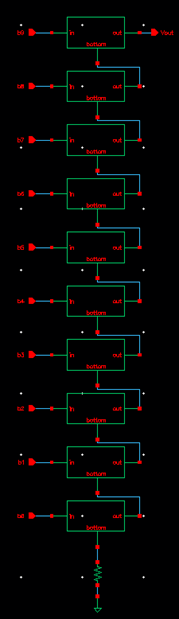
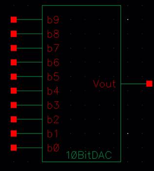
The next step in creating the 10-bit DAC was stacking and
connecting 10 of these symbols in the fashion seen in Figure 30.14. The
following snips show the schematic and symbol created from this process.
![]()
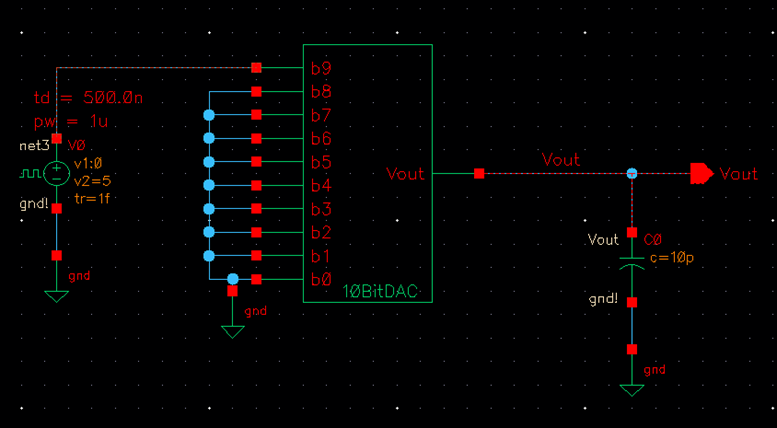
The expected time delay can be calculated
using the formula ![]() , where R is the equivalent resistance (R = 10k) and C is 10pF
(given in design requirements). Therefore,
, where R is the equivalent resistance (R = 10k) and C is 10pF
(given in design requirements). Therefore,
![]()
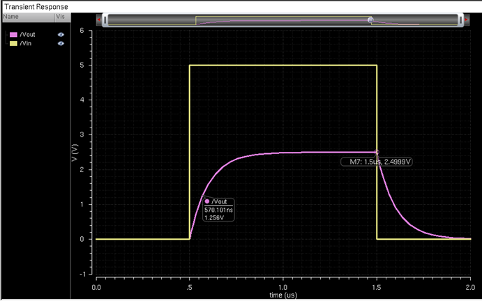
This is then proven correct through the simulation below. The time
when the capacitor begins charging is 500ns. The time marked below at
approximately half (1.25V) of the maximum voltage (2.5V), shown at 570ns. So,
570ns – 500ns = 70ns – exactly what we were expecting.
The following images show results under different load conditions.
Note that due to convergence problems, the simulations tolerance
options were changed to force convergence.
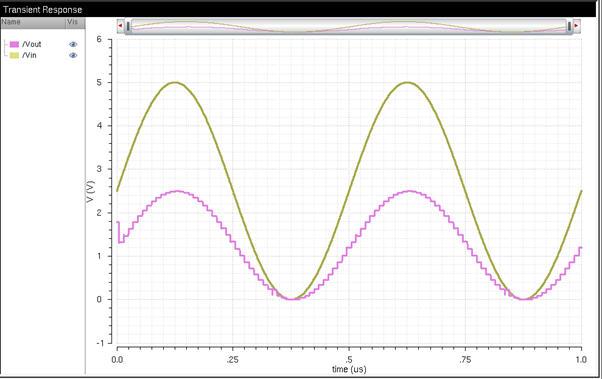
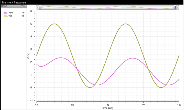
Under no load:
Under no load conditions, the digital signal follows the
amplitudes of the analog signal. This is to be expected, as the results should
closely match those of the ideal DAC (shown in the prelab).
Under a 10k resistive load:
The resistor in this load results
in a voltage divider. In this case, we are driving an equivalent resistance of
10k with a load of 10k, causing the digital Vout
signal to be half of the analog Vin signal.
Under a 10p capacitive load:
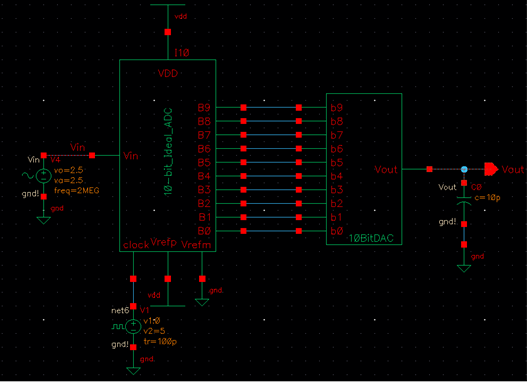
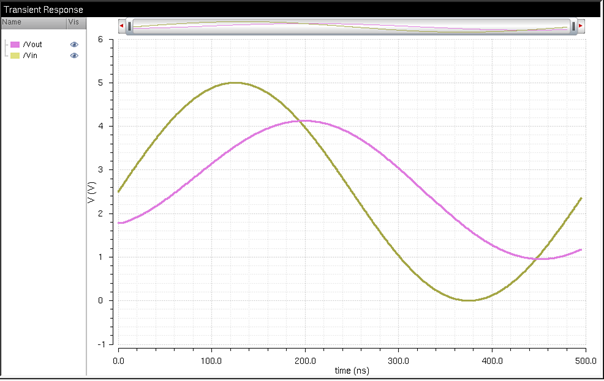
Under the capacitive load, the
delay the output signal shows is due to the 70ns time delay that arises when
the capacitor is charging (calculated previously). Additionally, the capacitor
smooths the square-like wave in the output, and there is a clear change in the
voltage swing - the input goes from 0V-5V while the output goes from
approximately 0.95V - 4.1V.
Under a 10k resistive and 10p capacitive load:
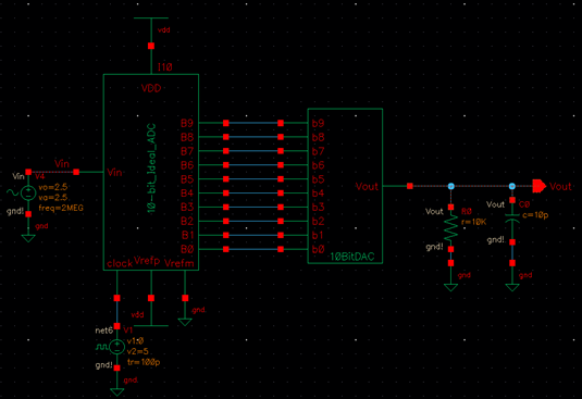
A resistive and capacitive load
will still show an output voltage that is approximately half the input from the
voltage divider, and there is a slight reduction in the voltage swing, as well
as a smoothed and lagging output caused by the capacitor.
If the resistance of the switches is not small compared to R, (ie. if the switches are transistors), the equivalent
resistance of the DAC would be different. The series resistances of each bit
would be higher, causing an equivalent resistance that is higher than R. A
higher resistance will result in a greater voltage drop across the transistor,
which would cause a smaller output voltage. This new equivalent resistance
would need to be calculated and accounted for in the load of the DAC.
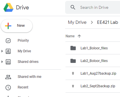
As my last step in this lab, I backed up my files the same way I
did in Lab 1. Below shows a backup of the lab work in my google drive:
This concludes Lab 2.