Project - EE 421L 

Author: Edgar Amalyan
Email:  amalyane@unlv.nevada.edu
Date:   11/18/2020 (Design and Characterization) & 11/25/2020 (Layout)

Goals:
This project will consist of designing, characterizing, and laying out a High-Speed Differential Amplifier.

Introduction  

Note: Please click on pictures for larger views.
Note: All design files can be found here.

Logic Signals
Digital electronics are based on signals that are either a 0 (low) or 1 (high). We know that all digital signals are physically analog signals. This means that low can be represented as 0V and high as 5V. But what happens if the signal is not exactly 0, or not exactly 5? What if logic high is theoretically designed to be 5V, but in the real world ends up being 4V? Will the circuit that the input is fed into still operate properly?

Ethernet
Let's take a practical example of network data being transmitted over an ethernet cable. Information is transferred using packets of 0's or 1's. Consider the transmitter being told to send 0V for a 0 and 5V for a 1 over the cable. If the cable is a few feet in length, then the voltage level of the logic 1 on the receiving end could be 4.8V. This could be acceptable to the receiver. But what if the cable is 100ft long? What if the wires are high gauge copper? The resistance of the cable increases in both situations. Can we predict the voltage levels on the receiving end? Can the receiving circuit differentiate between low and high?

Differential Pairs
To counteract the effects mentioned above, differential signaling is used. One voltage level represents logic low, and its complement represents logic high. The receiver is now built to amplify the difference between the two signals. If it receives 1V and 2V, the amplifier in the receiver produces 0V and 5V, or whatever levels the component/circuit the amplifier is driving accepts. Our goal is to design this amplifier.


Design

Now that we have discussed the advantages of differential signaling, let's try and design an amplifier to perform this task.

We can start with Figure 18.17 in the book.

N-Flavor
A concise transistor level schematic of the N-Flavor input buffer is seen below.

N_Flavor_Sch.png

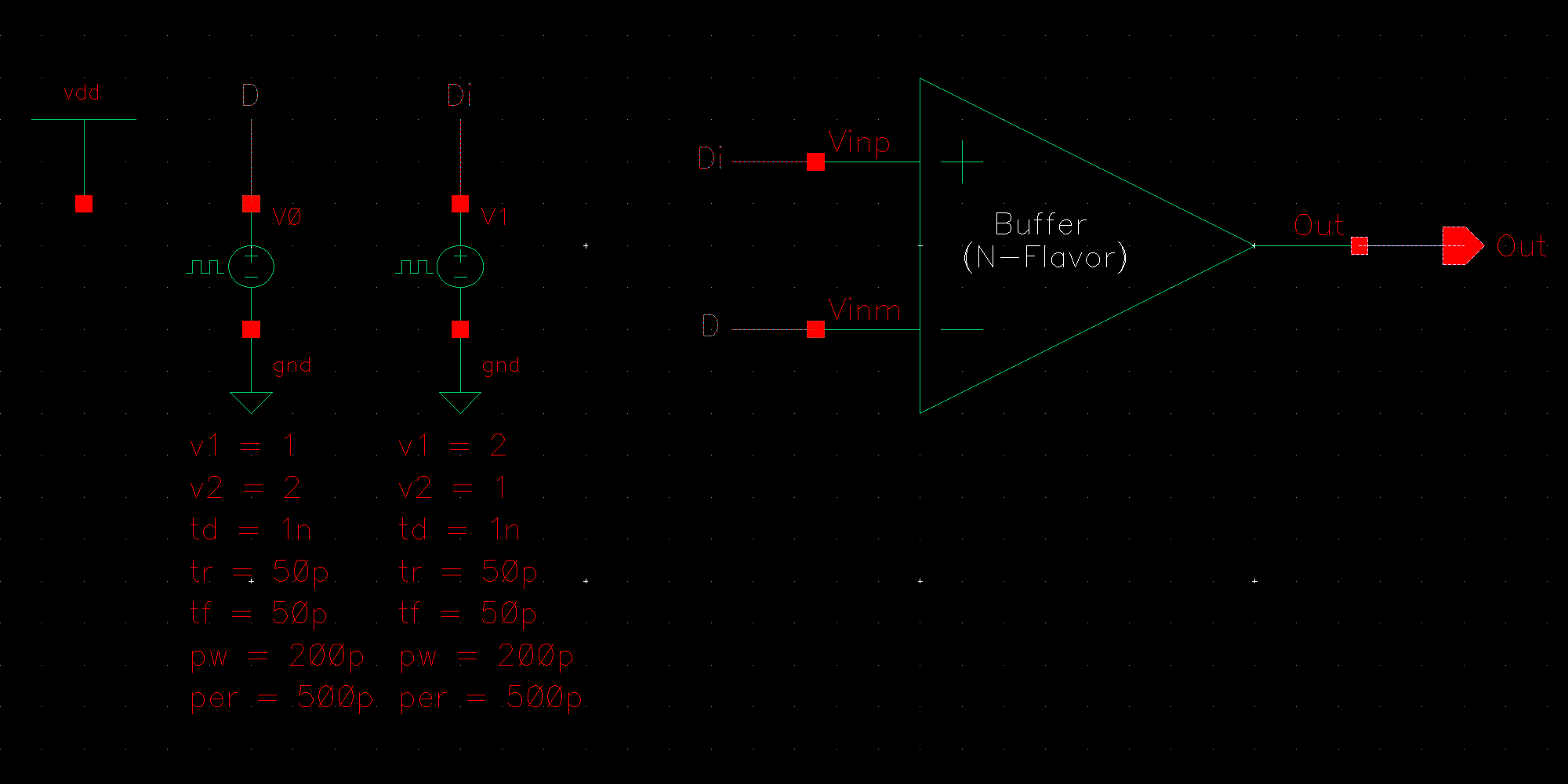
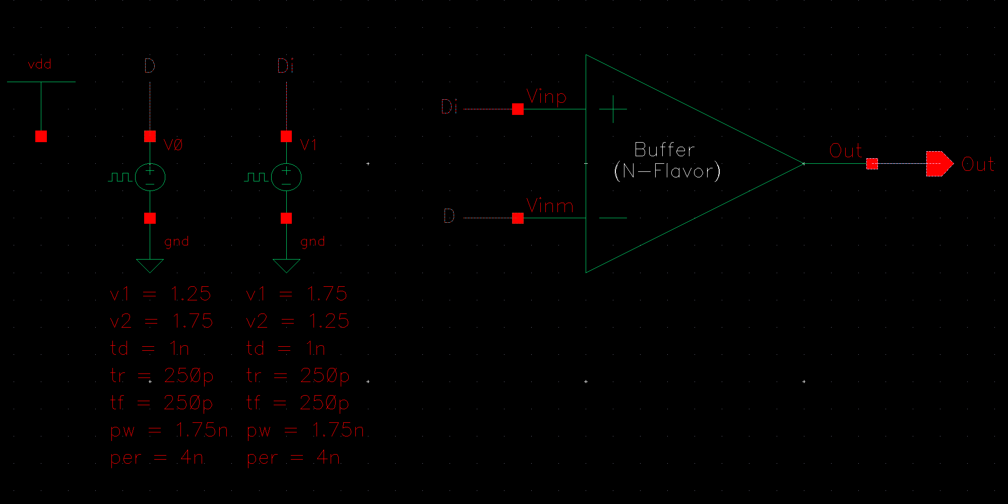
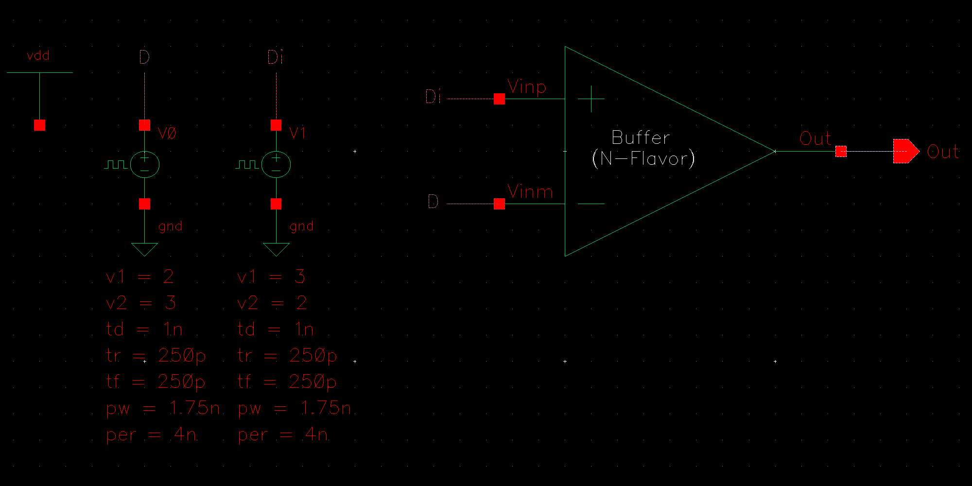
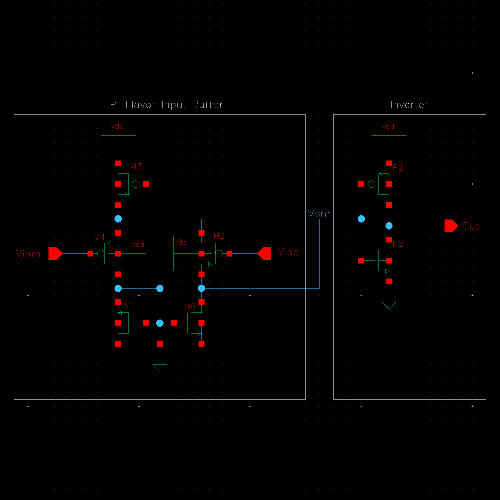
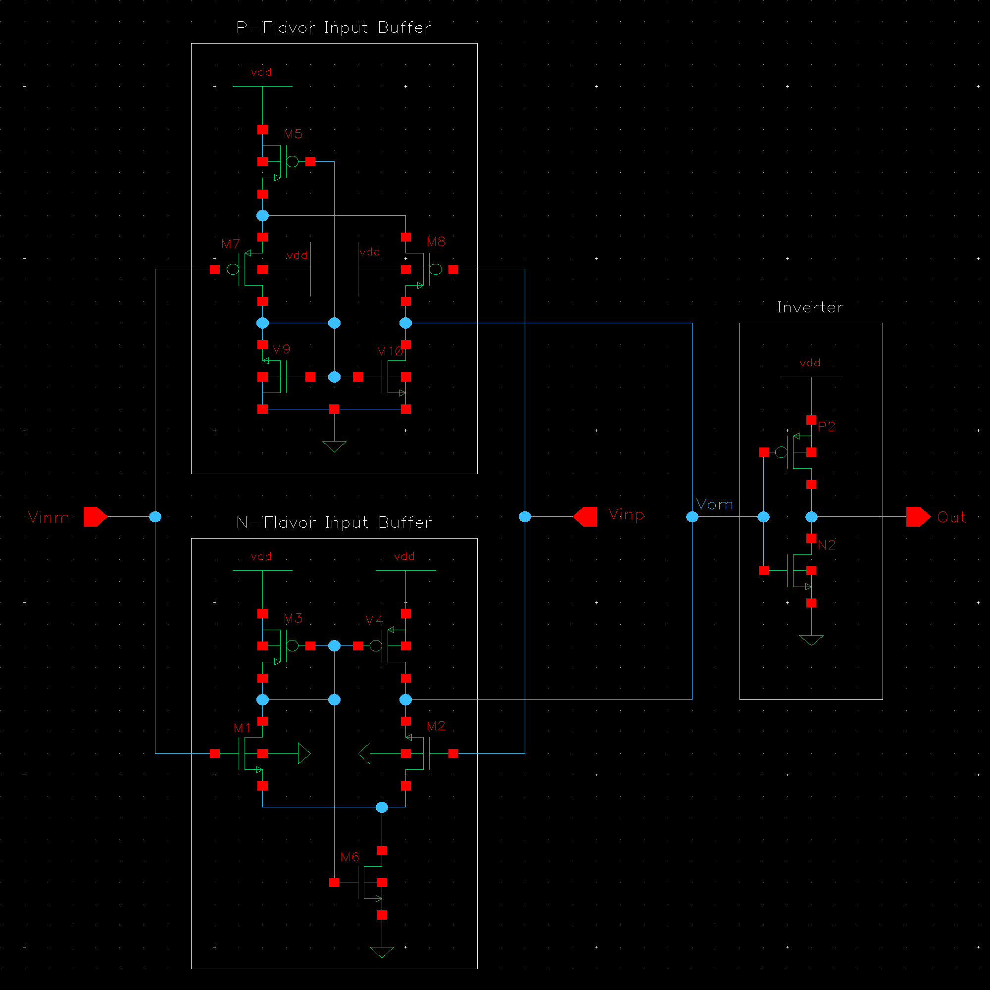
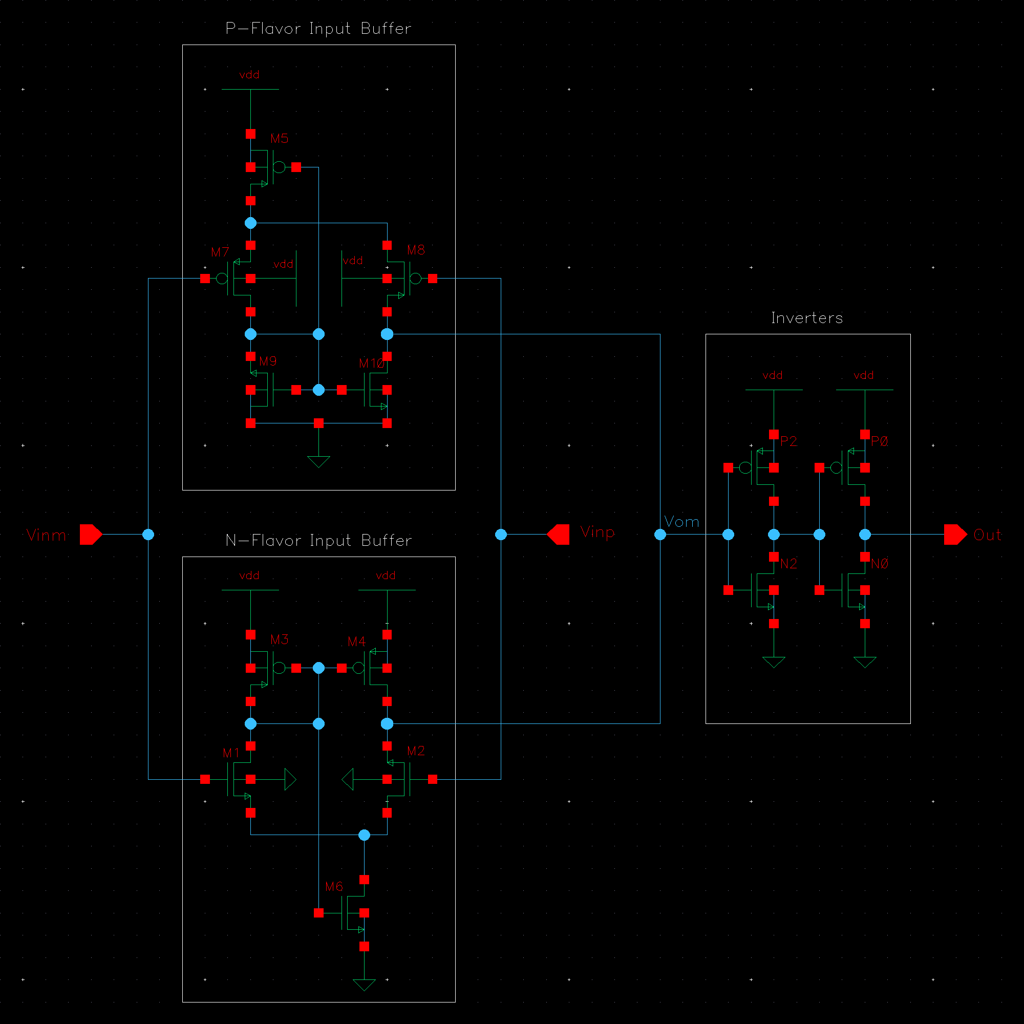
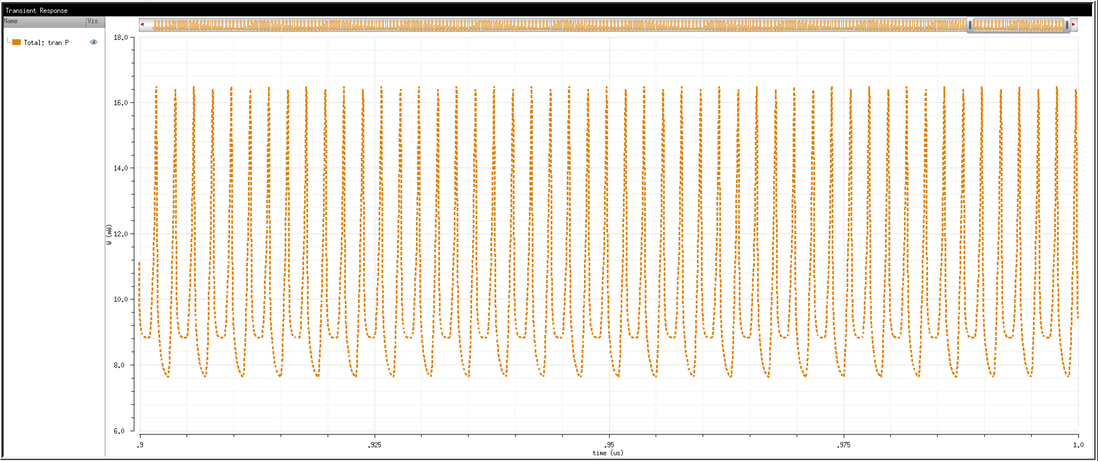
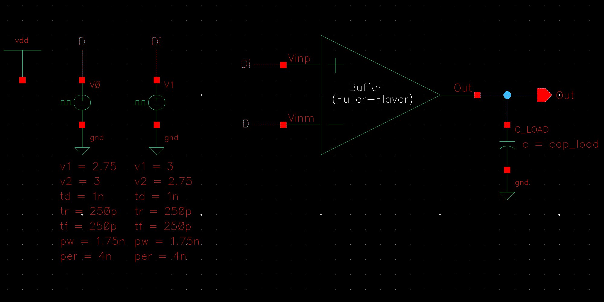
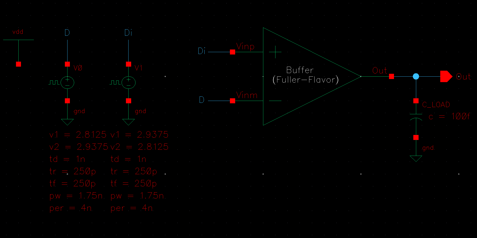
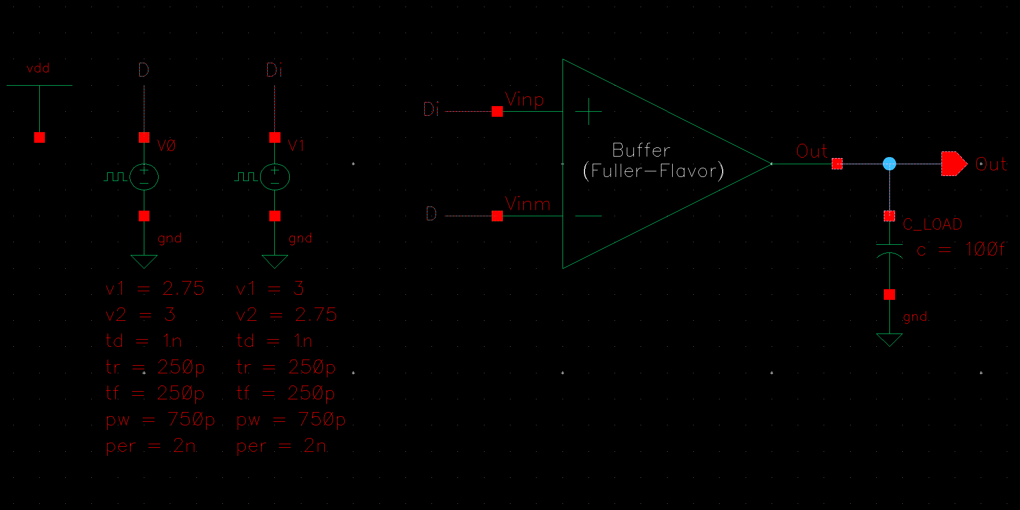
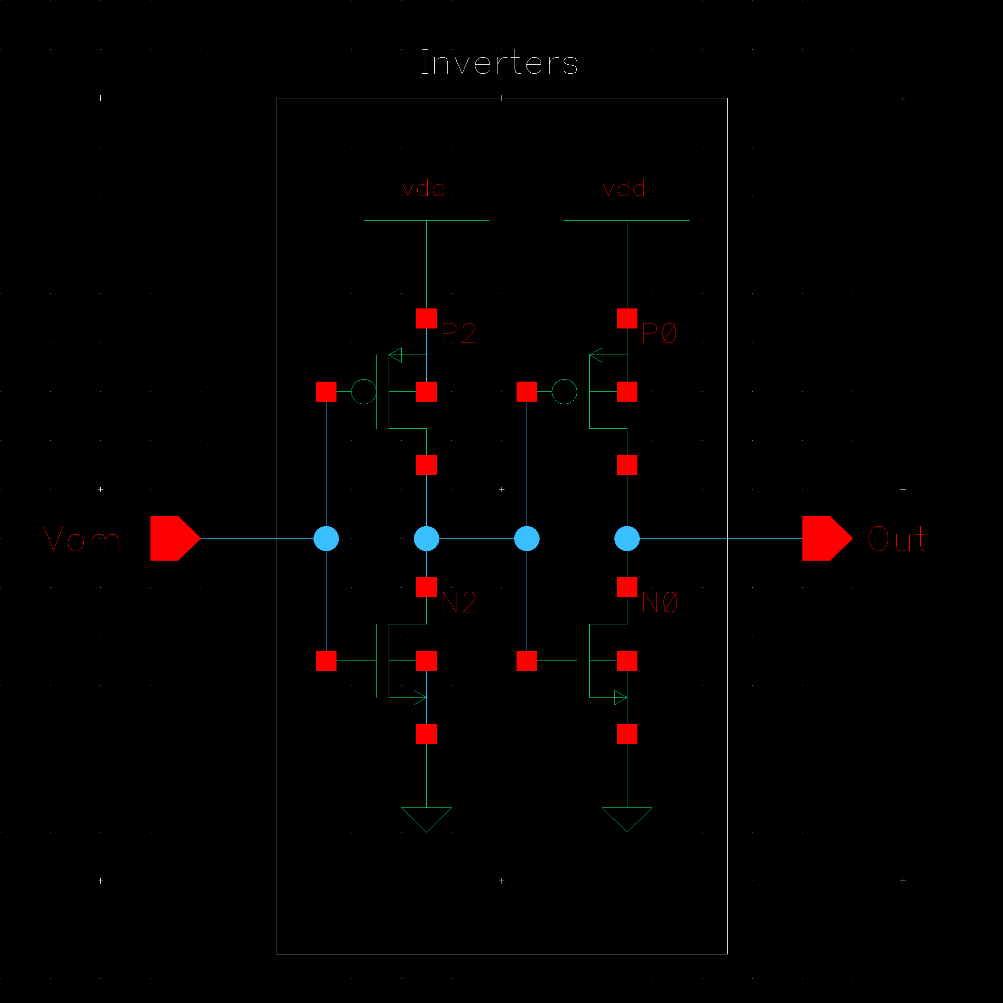
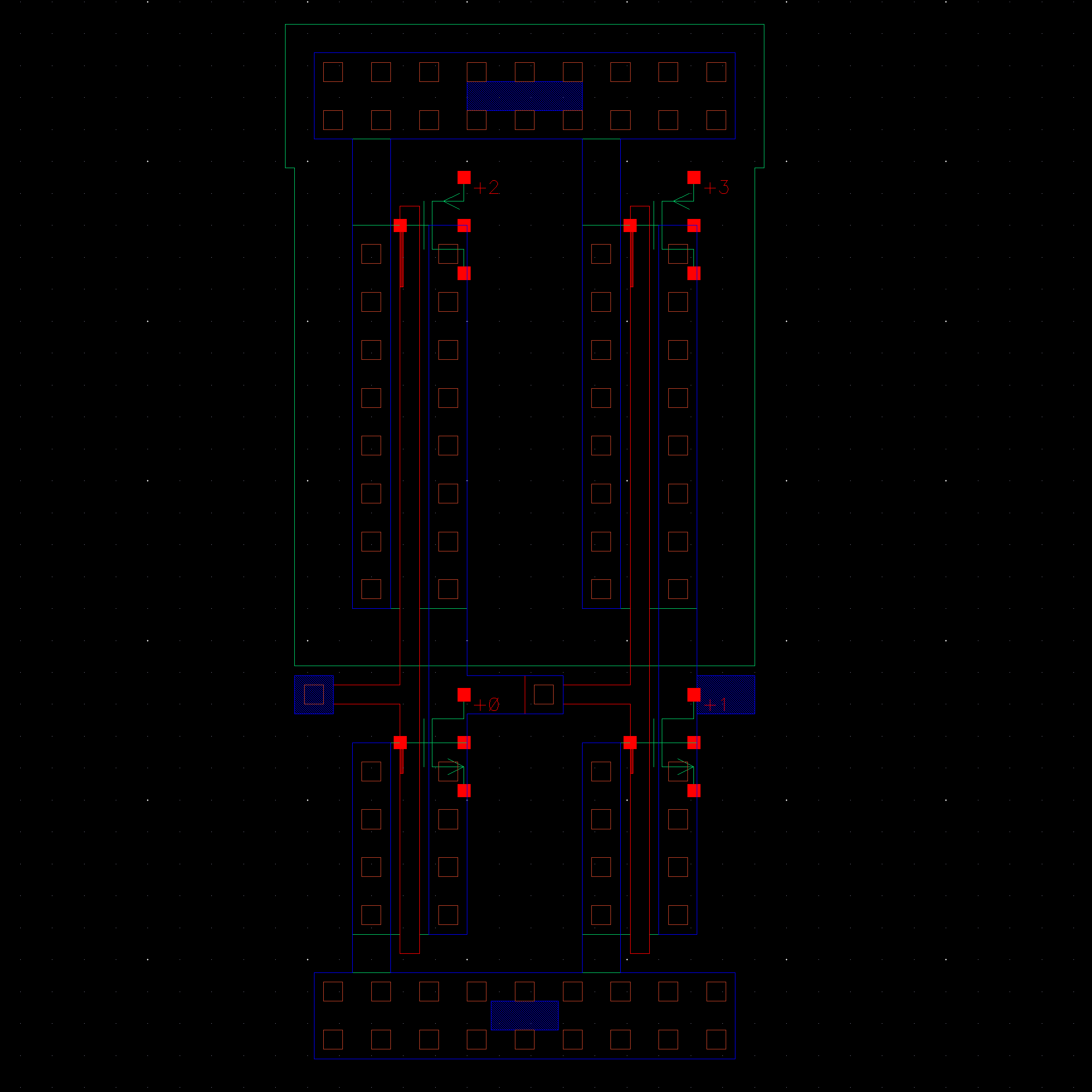
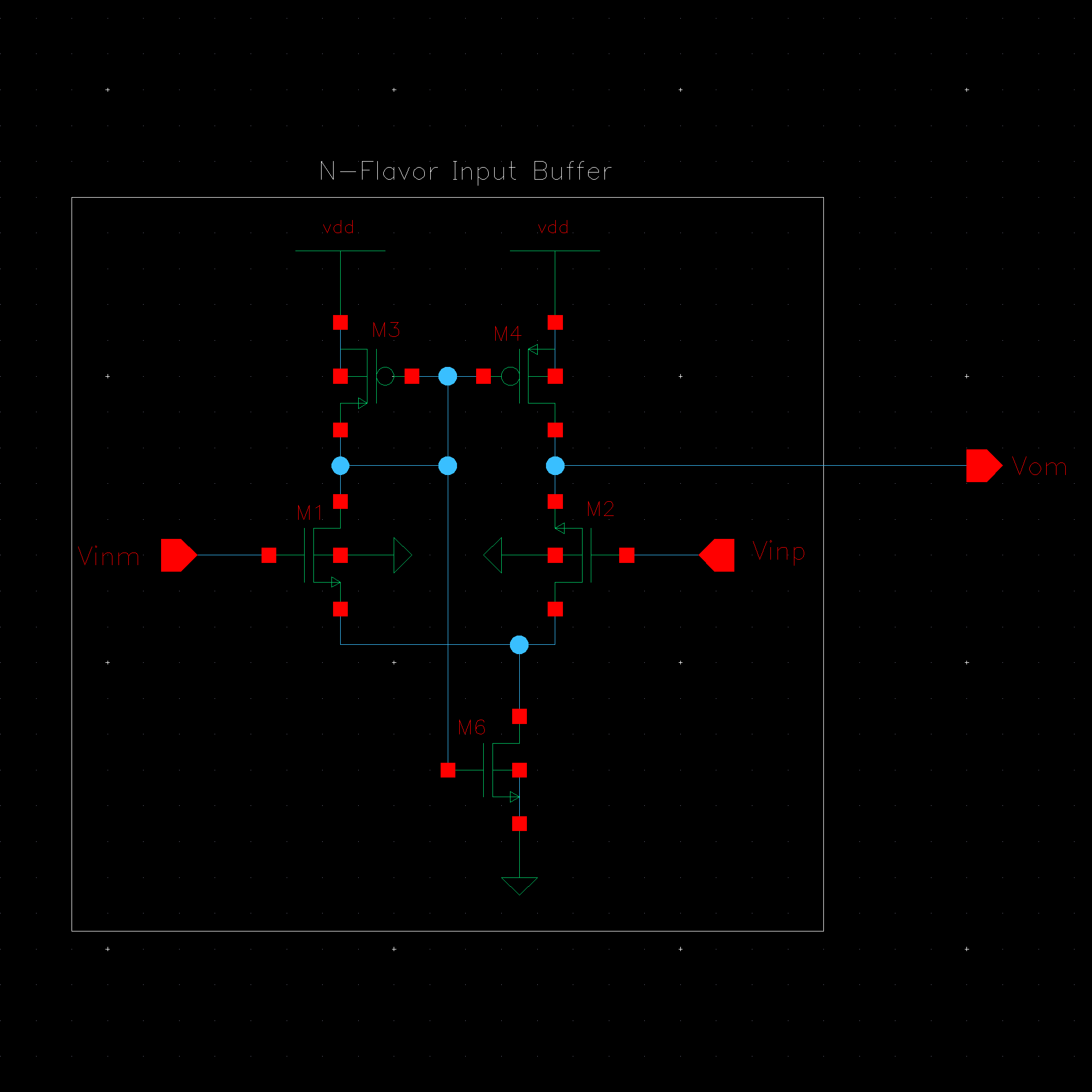
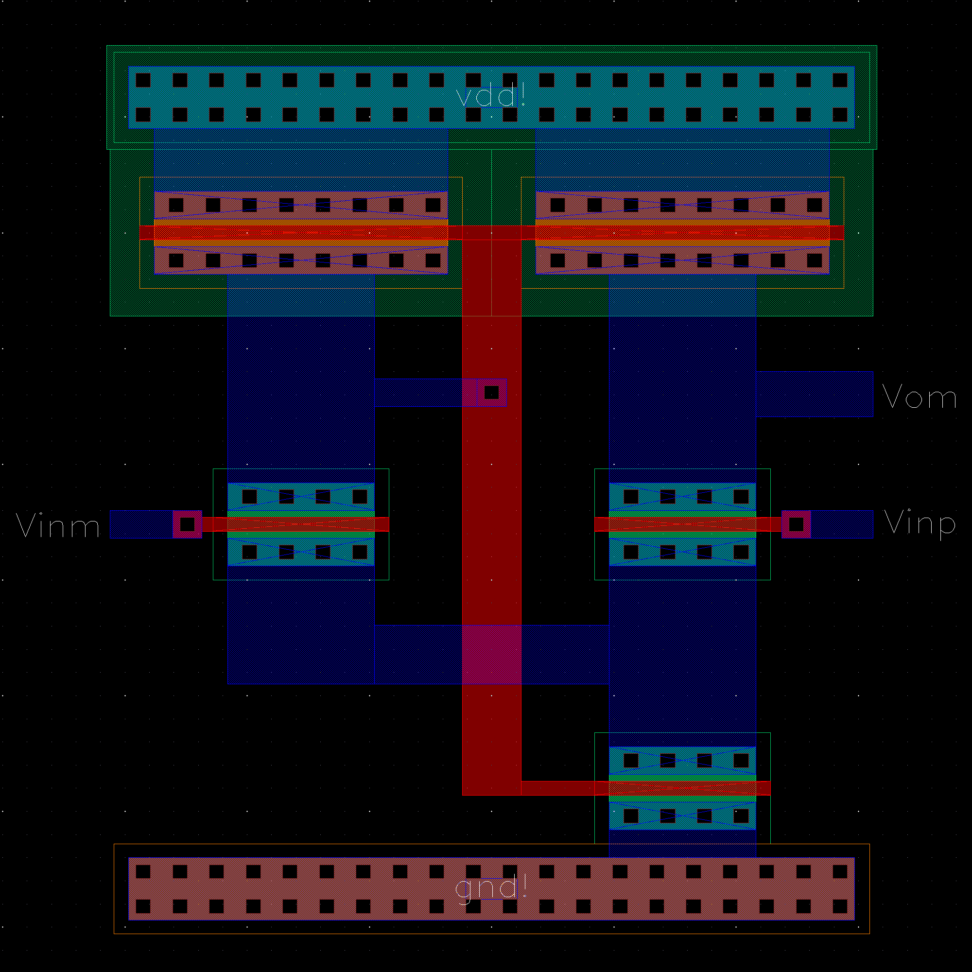
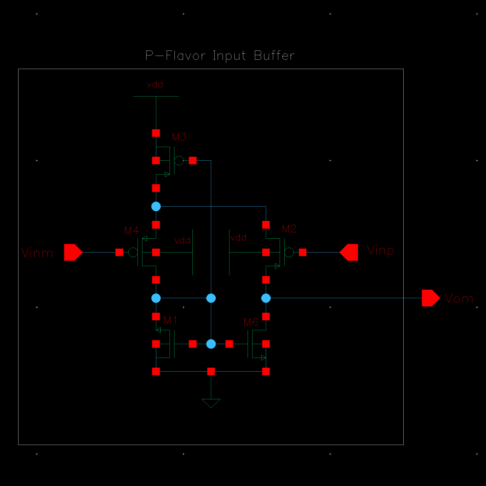
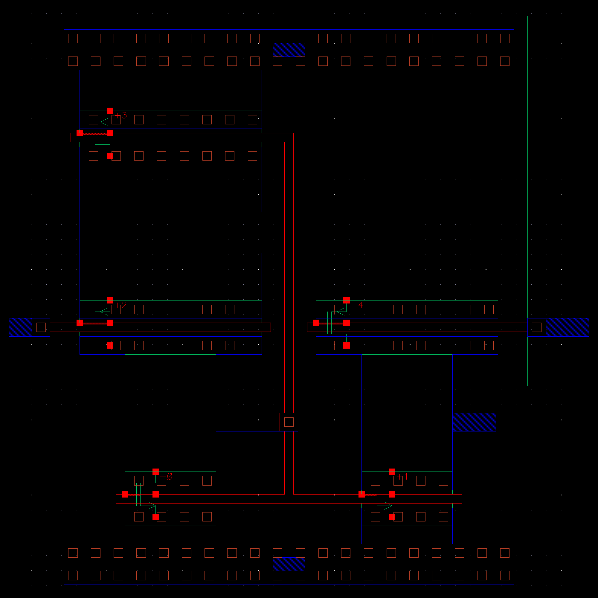
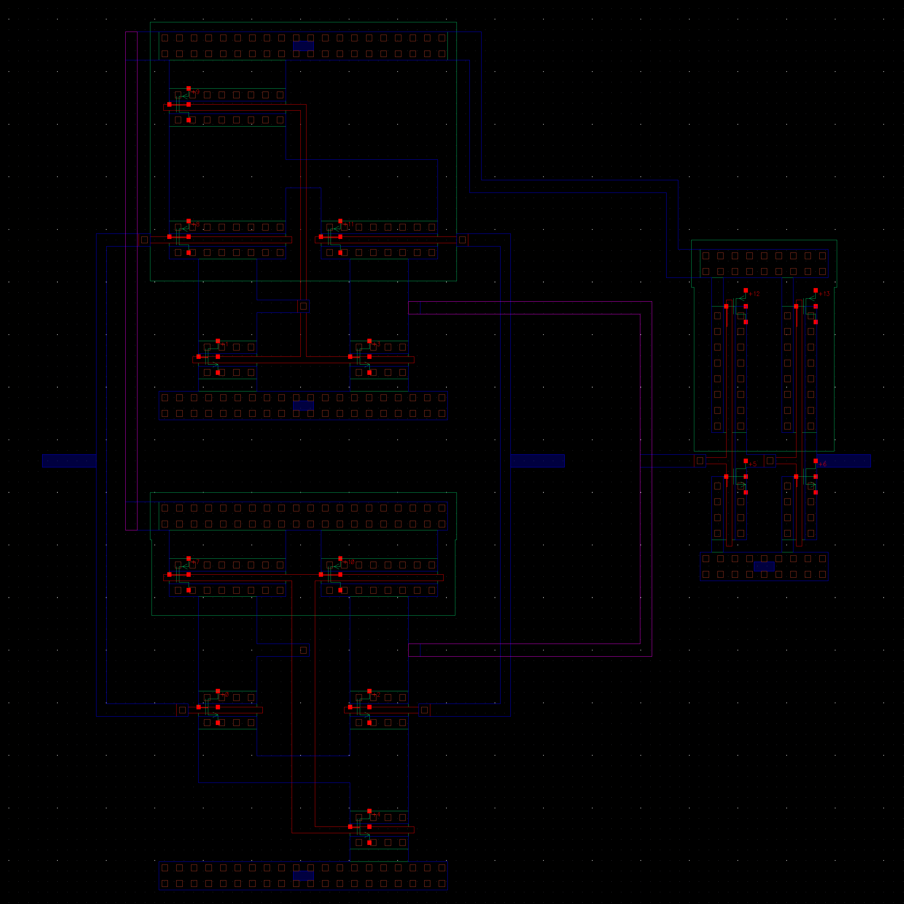
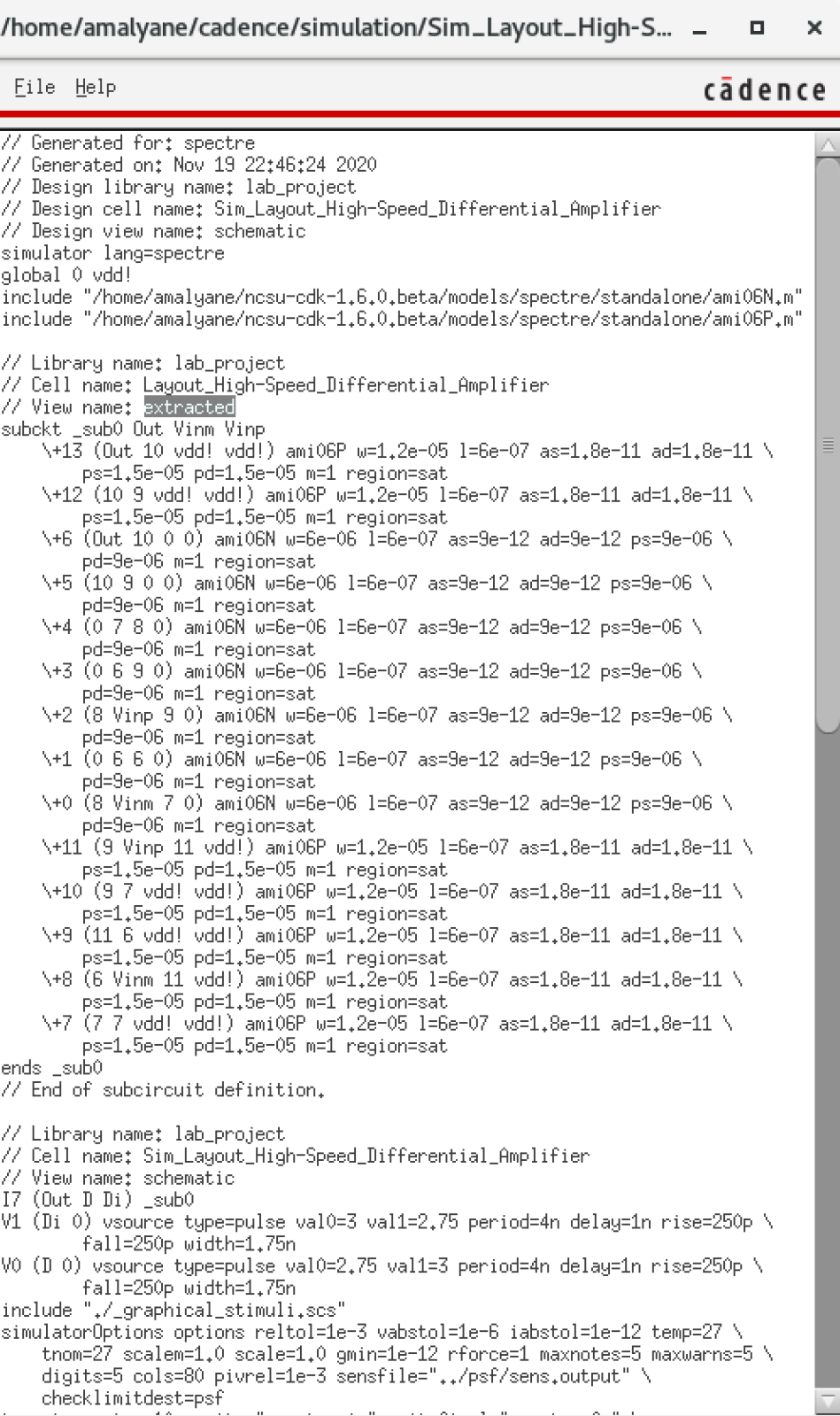
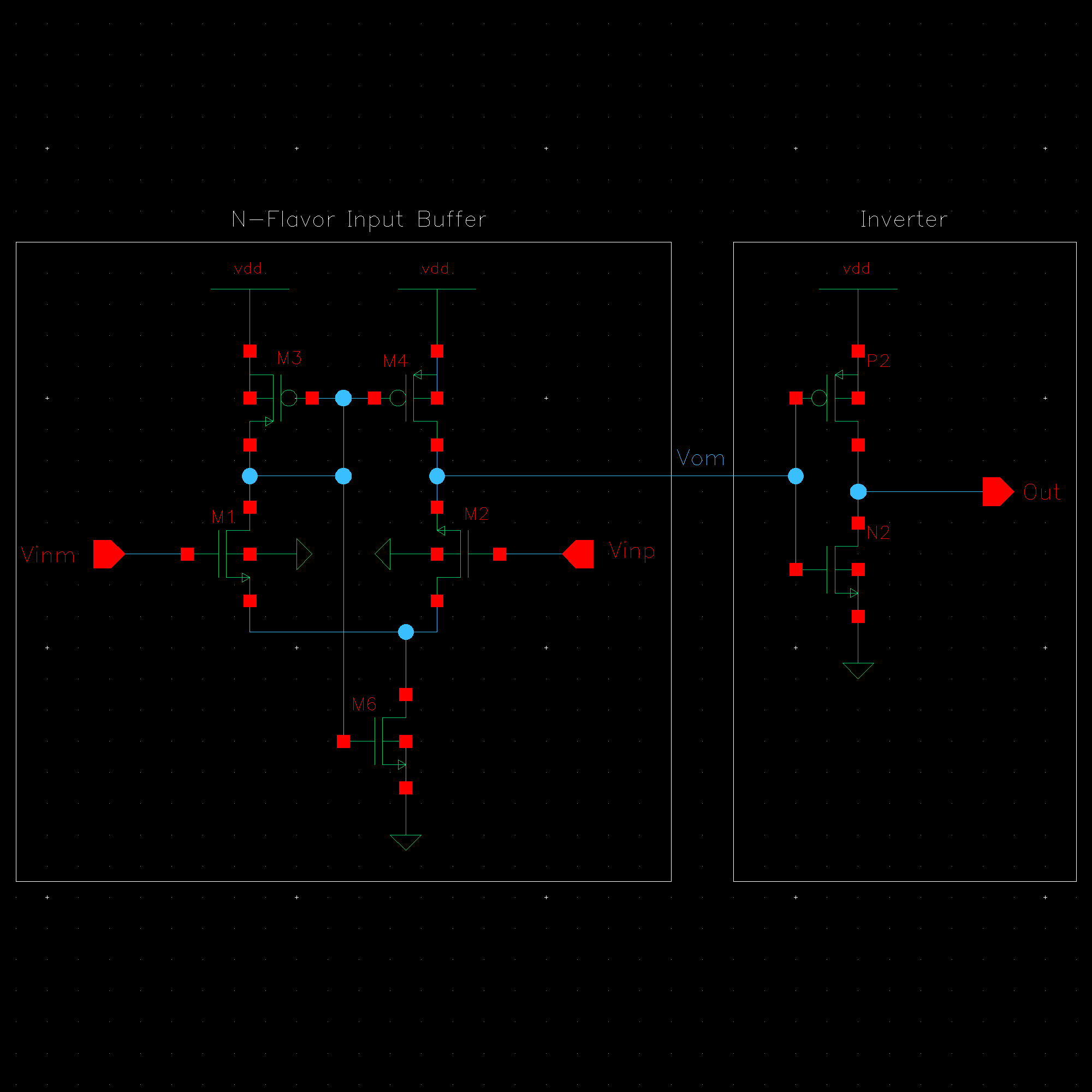
NMOS are 6u/0.6u and PMOS are 12u/0.6u.

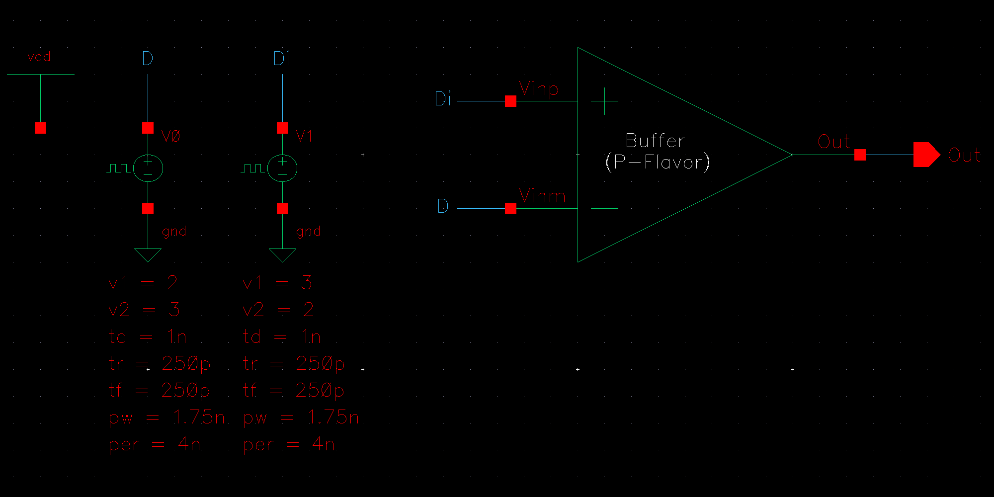
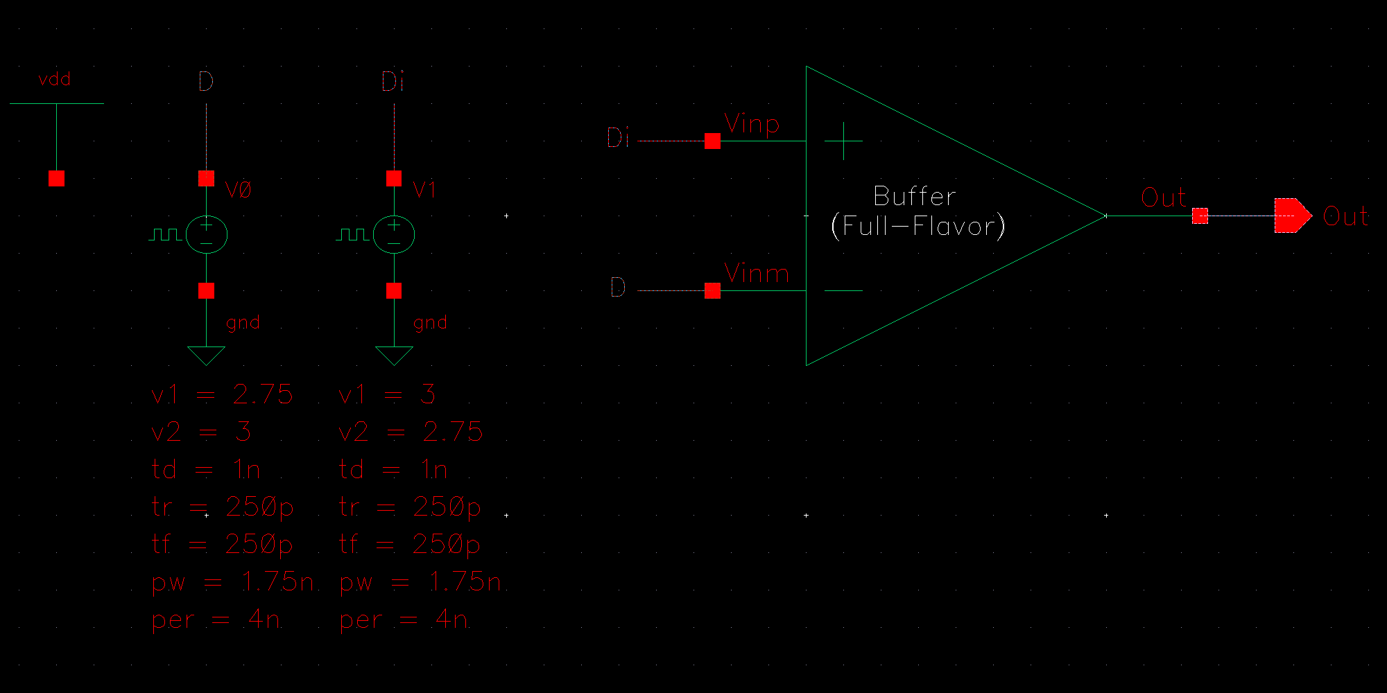
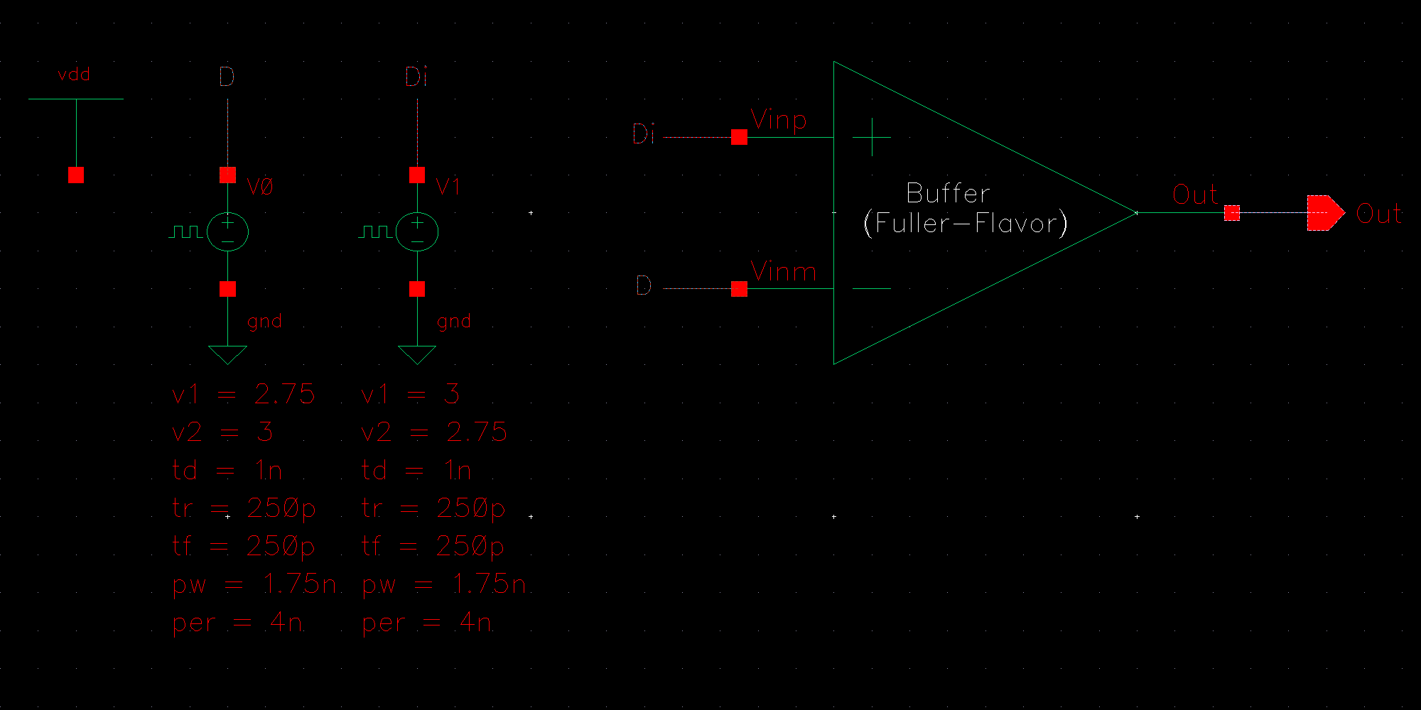
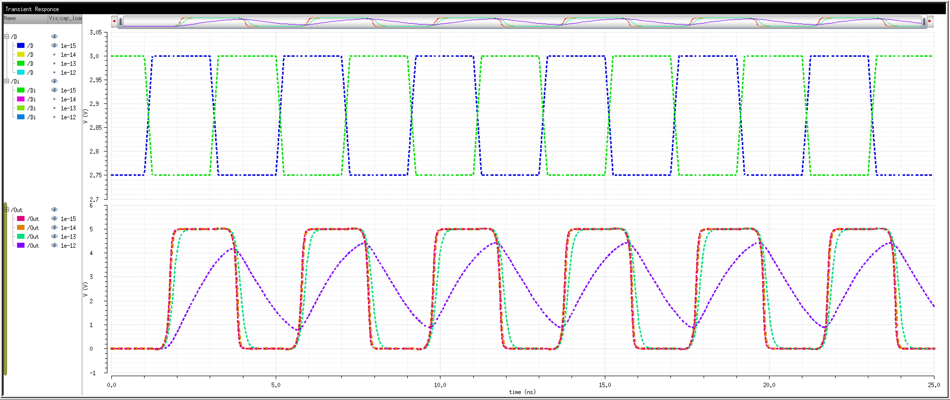
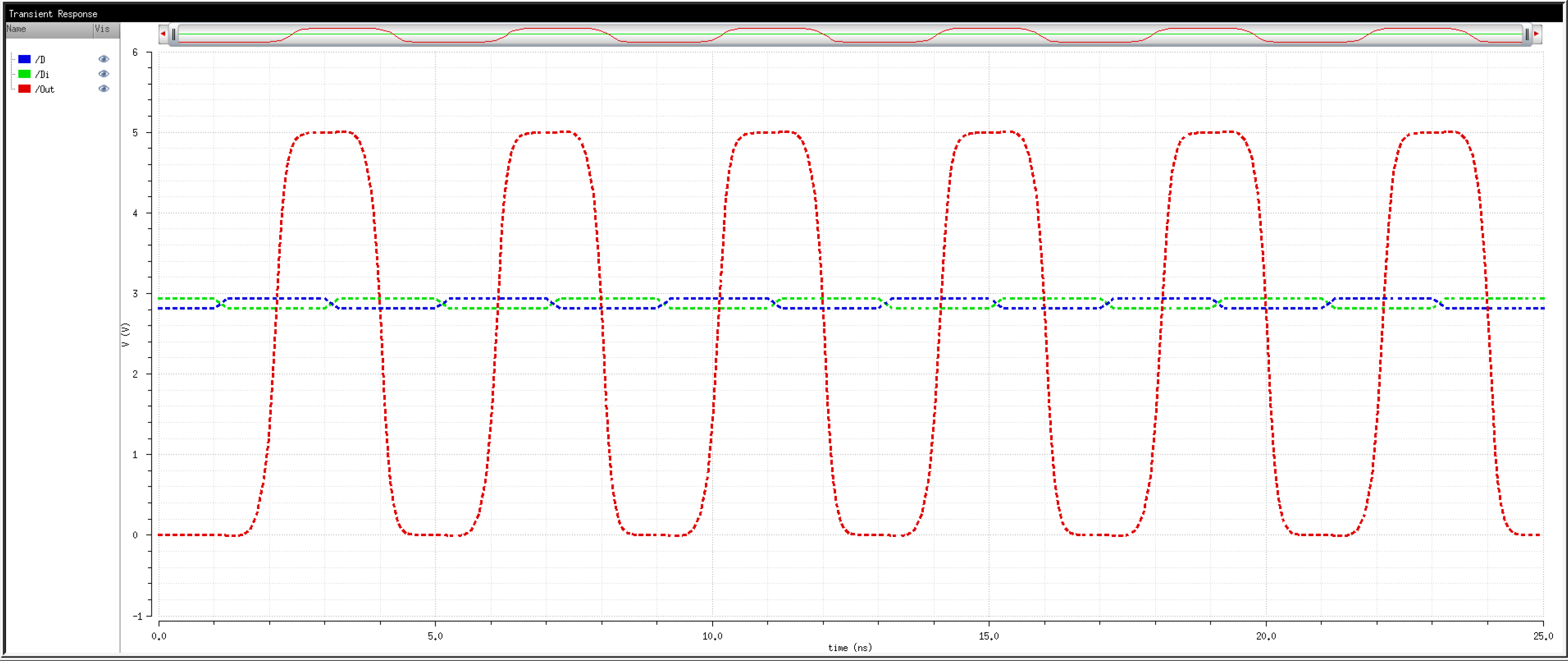
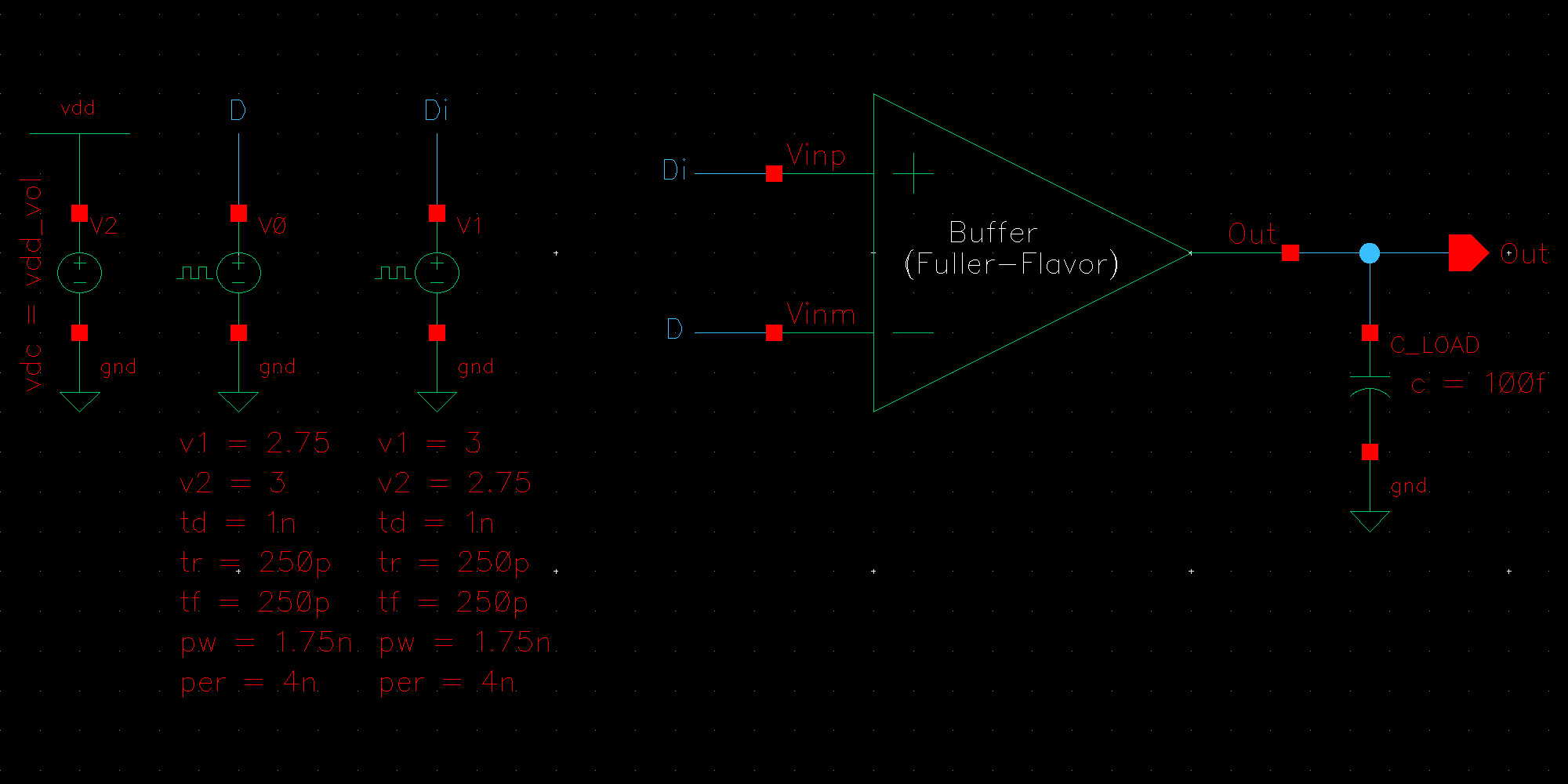
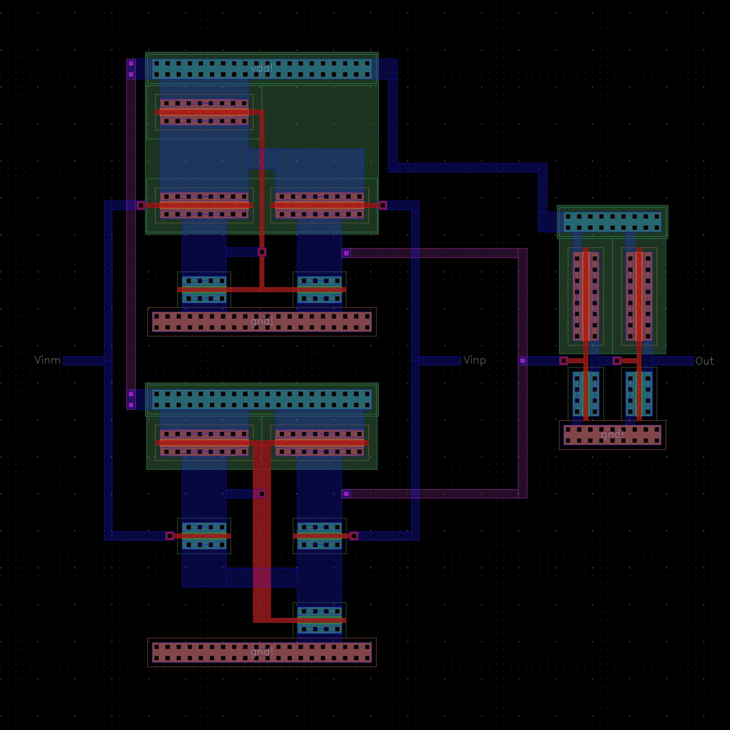
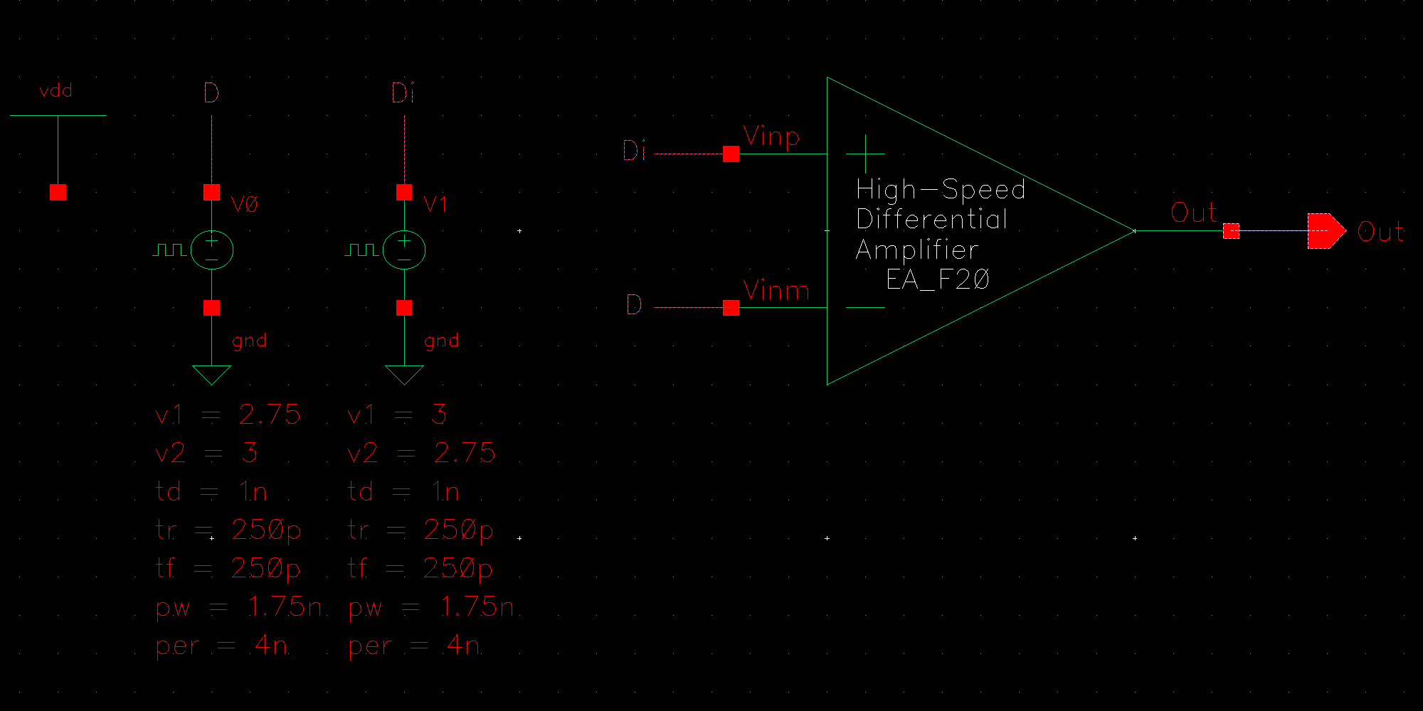
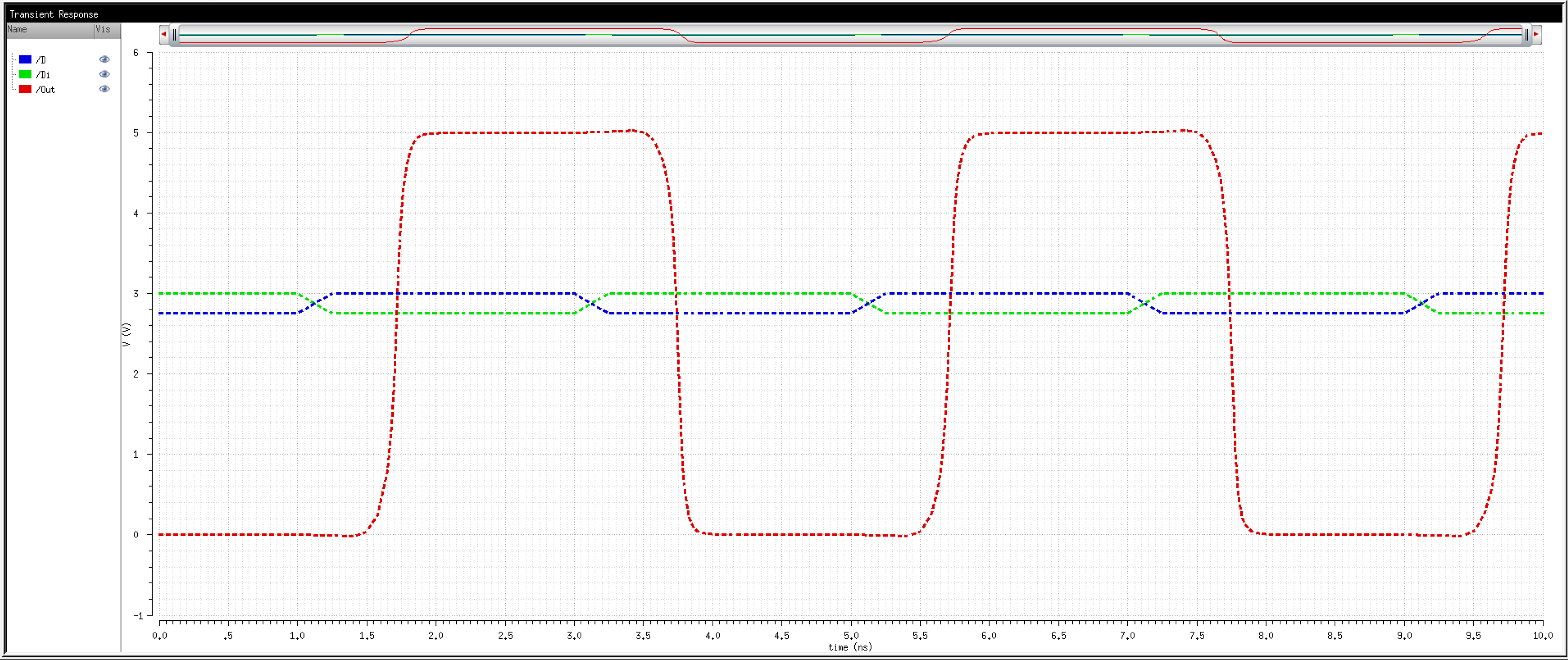
The detailed operation of the circuit is described in the book. Let us take the high level approach and consider that the circuit does what it is designed to do; take in an input and its complement and amplify the difference between them.
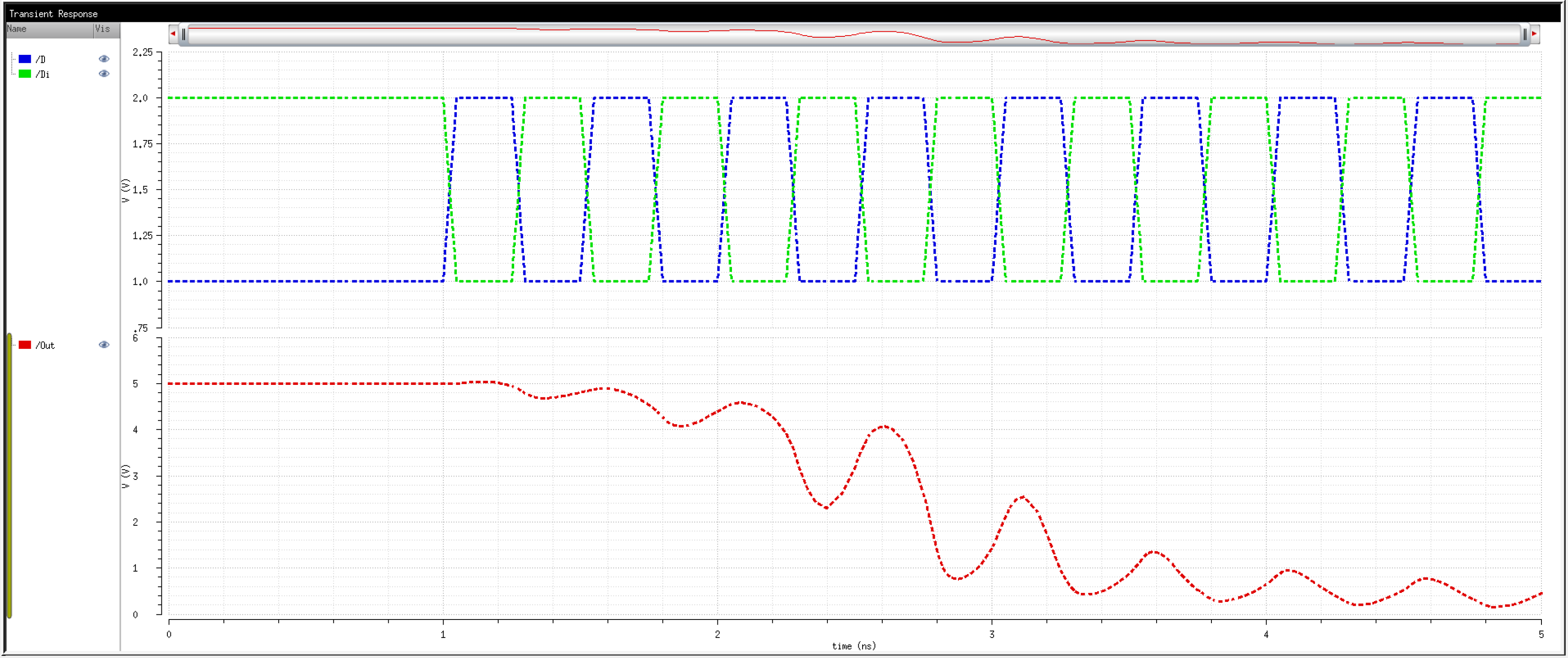
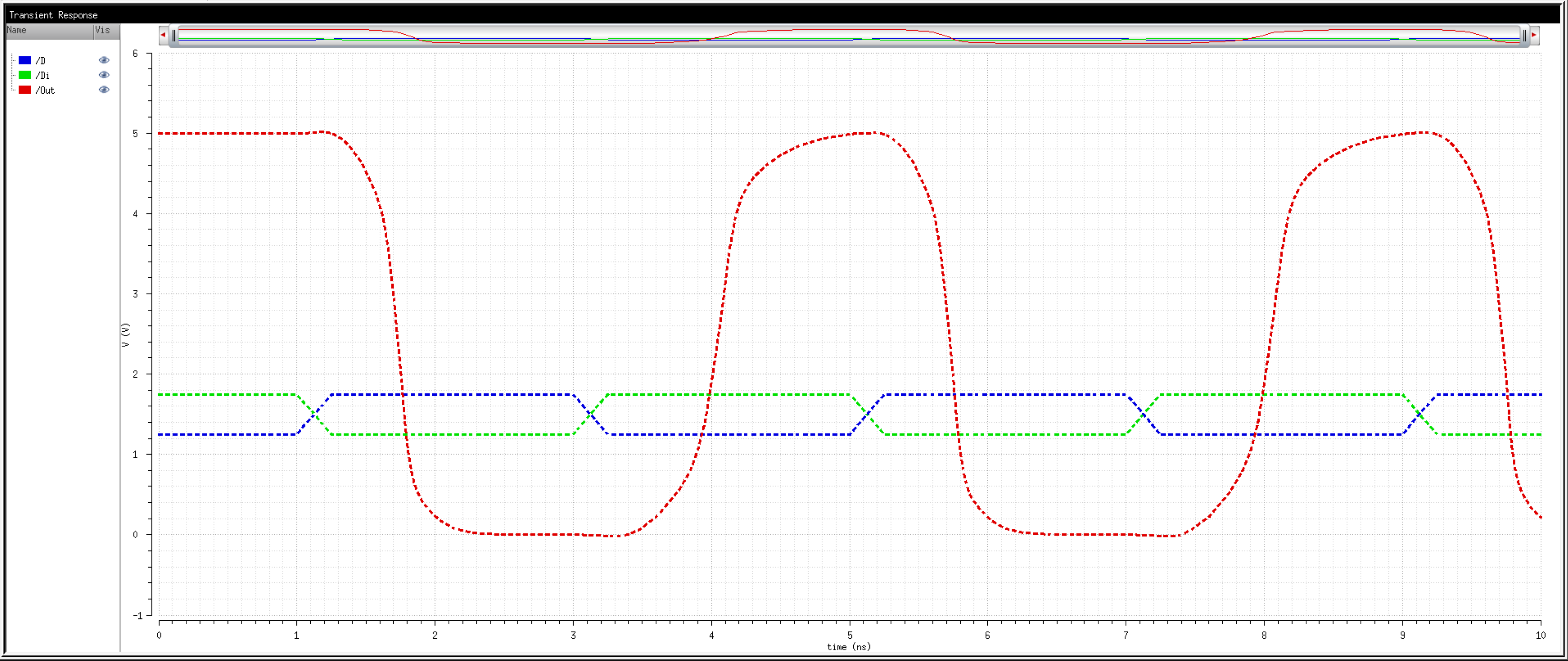
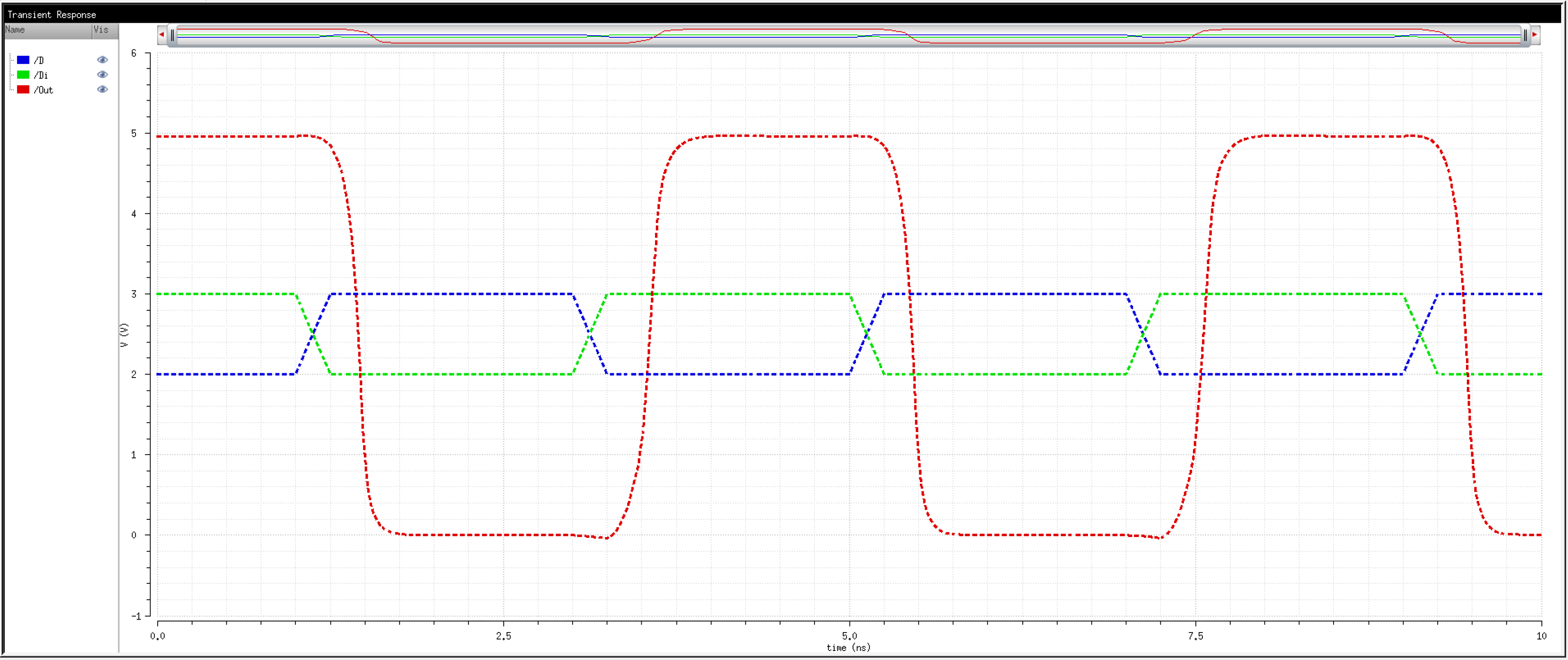
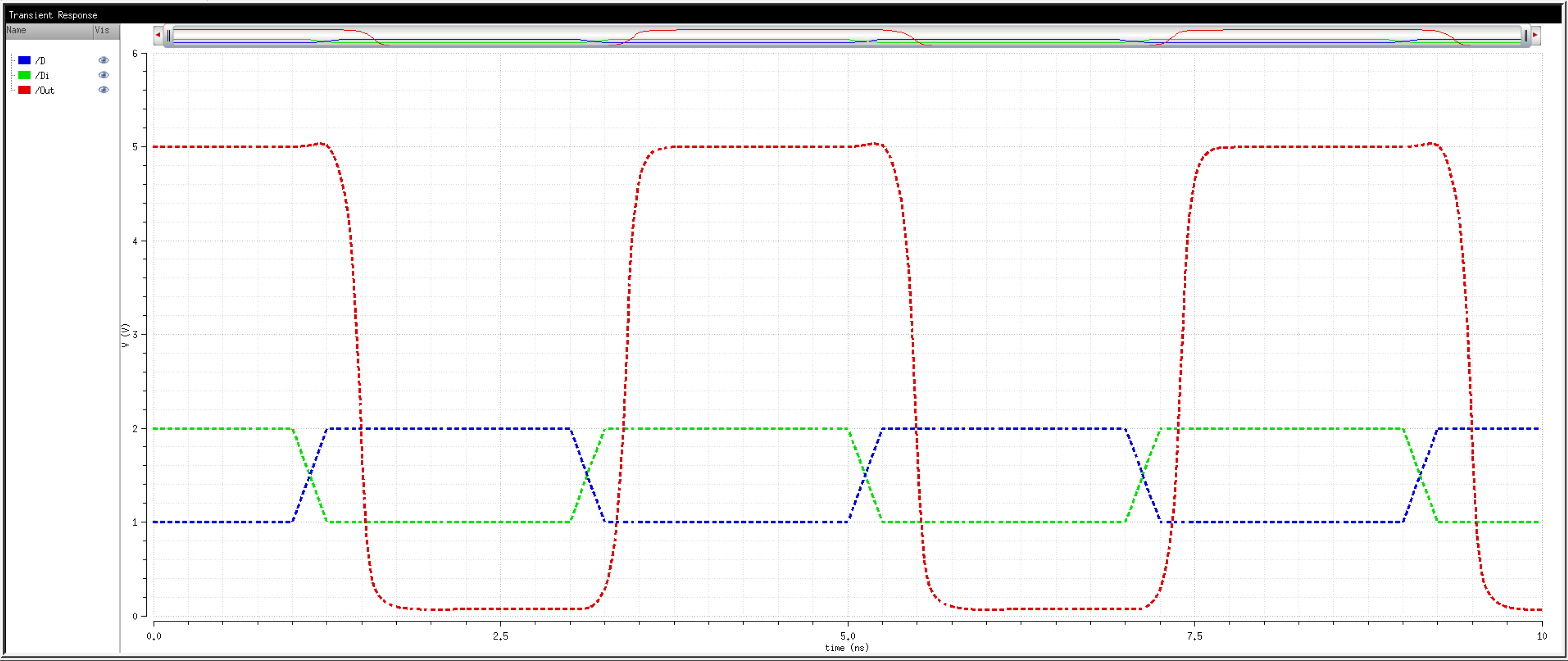
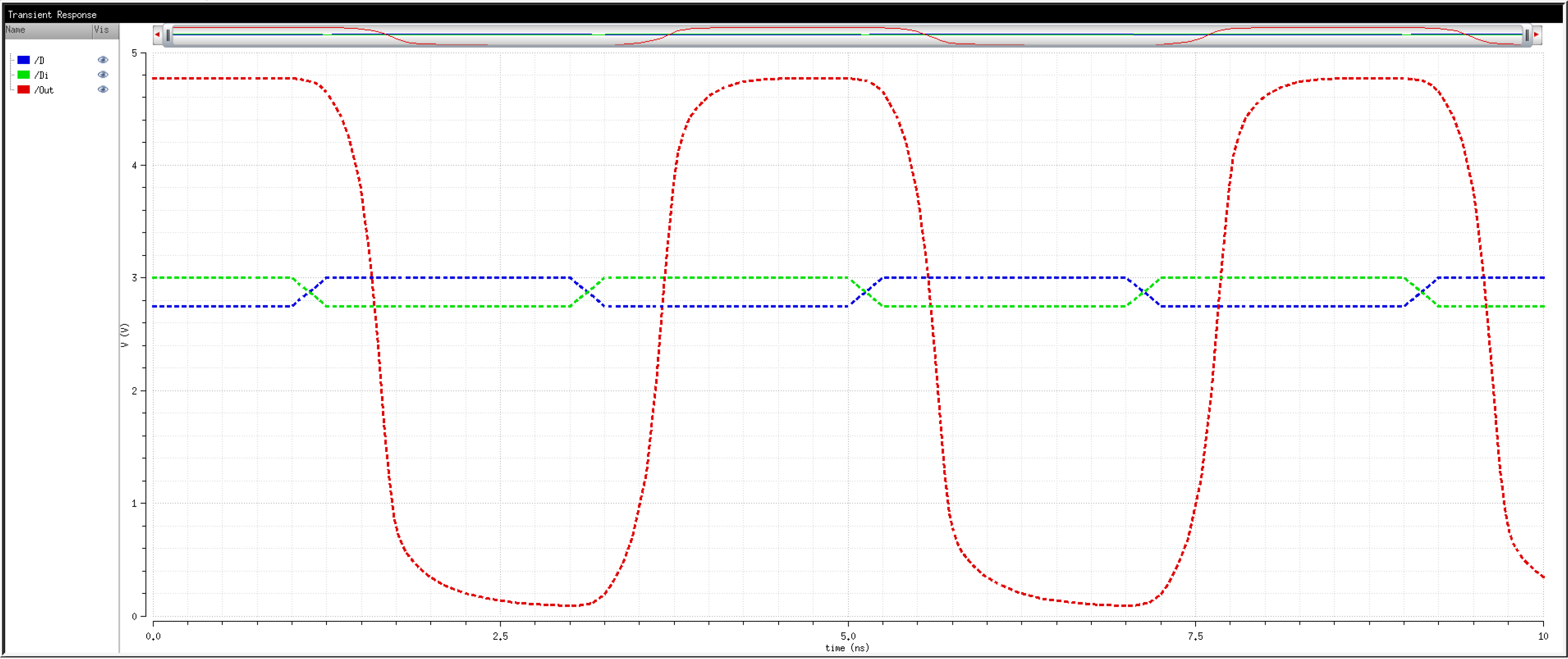
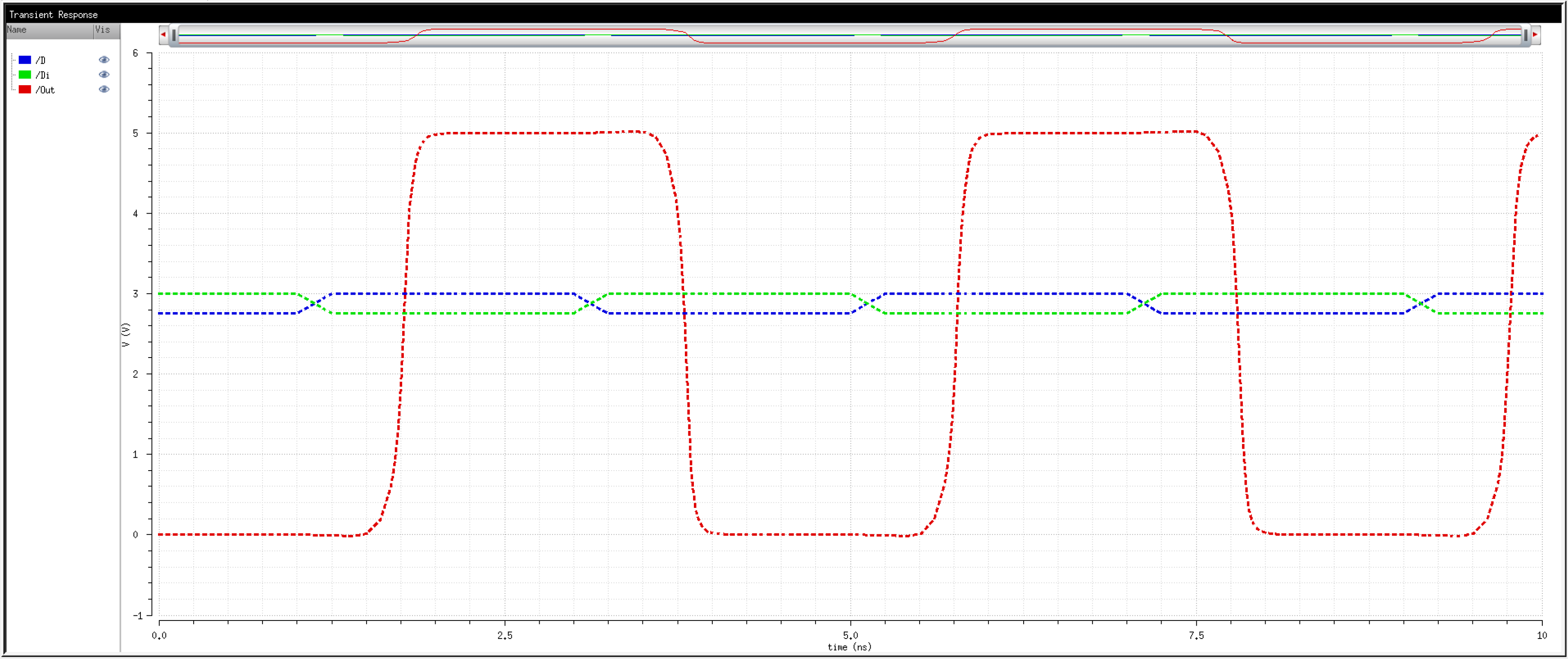
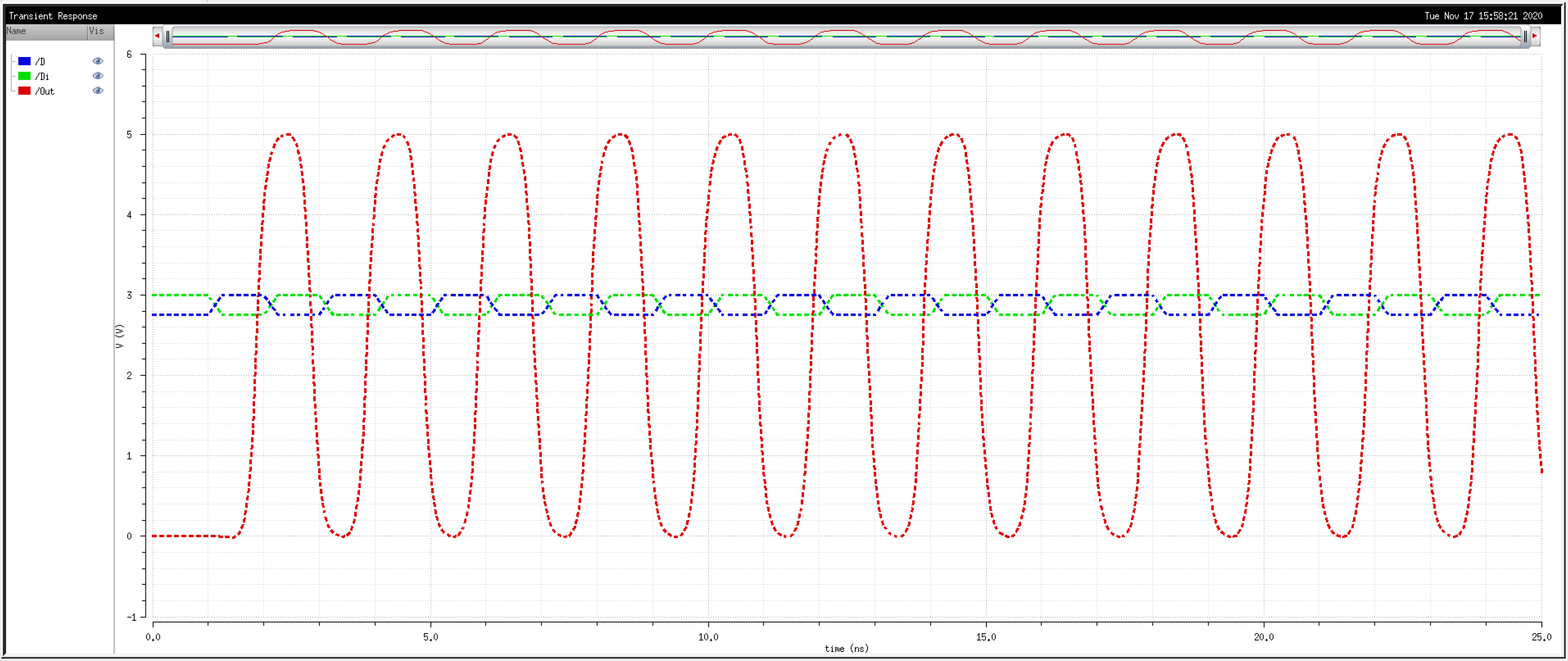
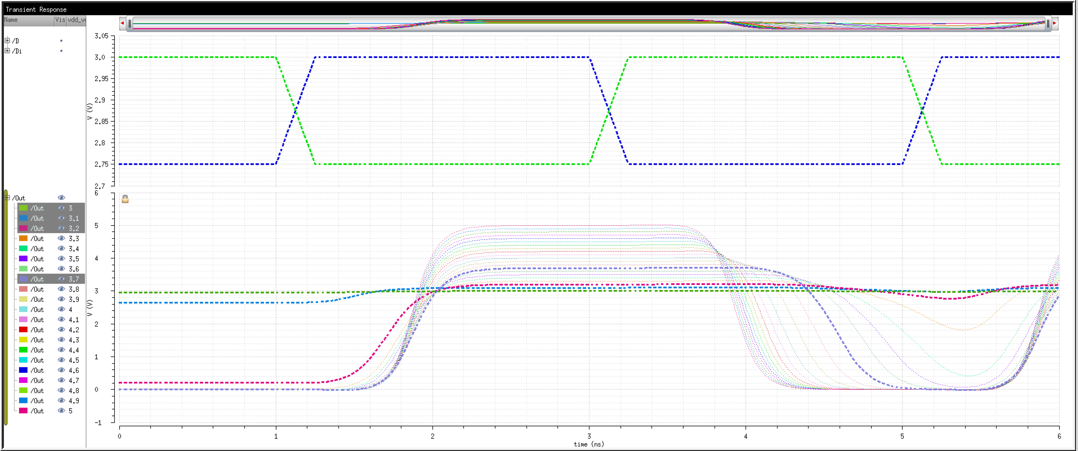
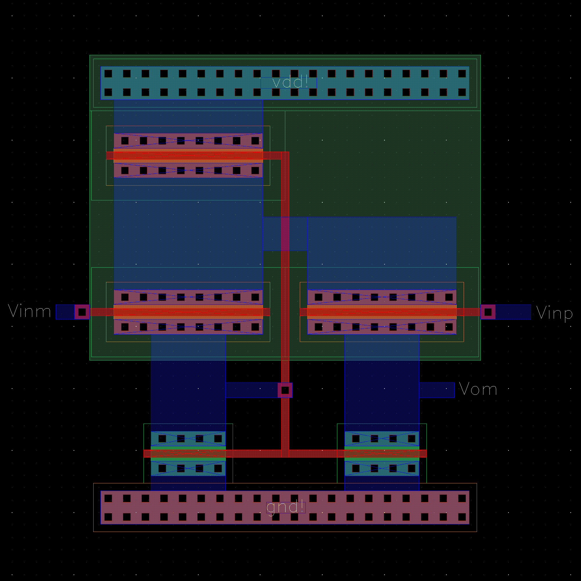
We know that transistors are real world devices and do not switch instantly. There is an associated delay contributed by the MOSFETs' resistances and capacitances.

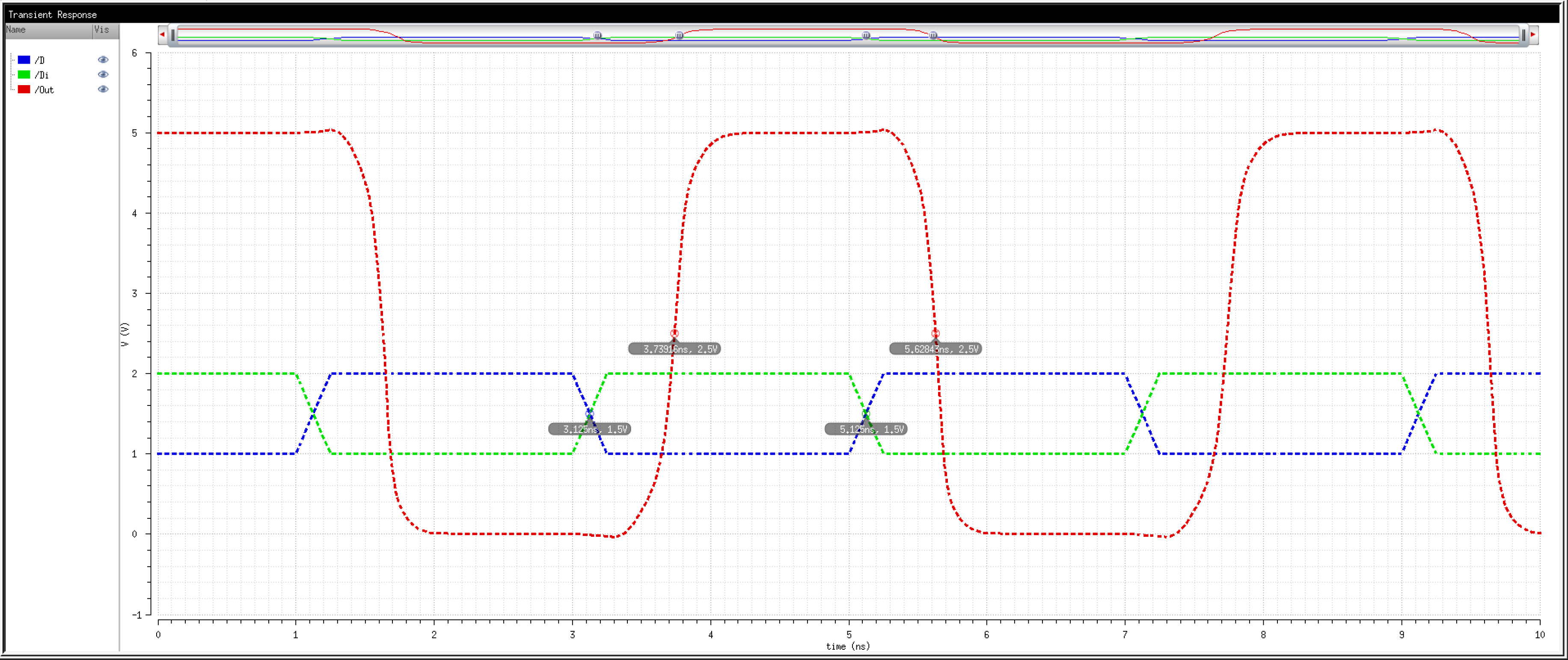
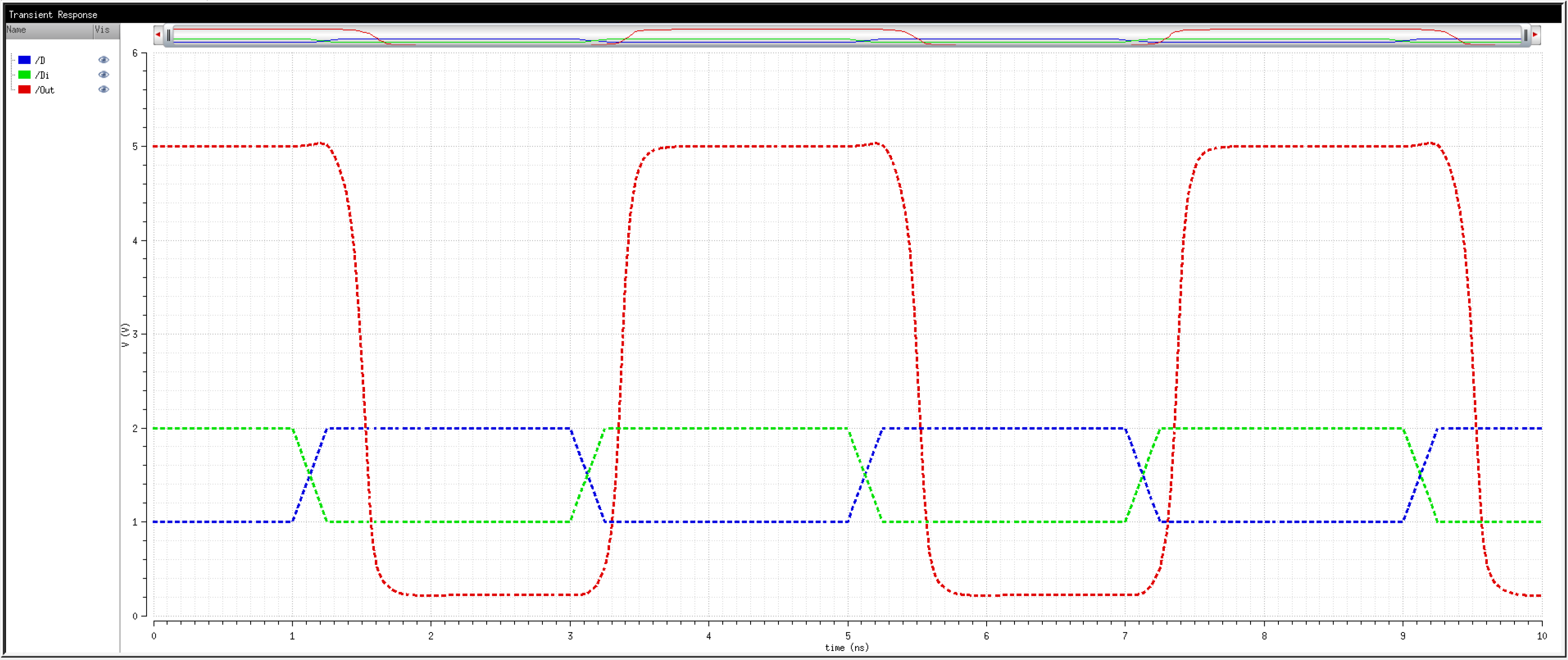
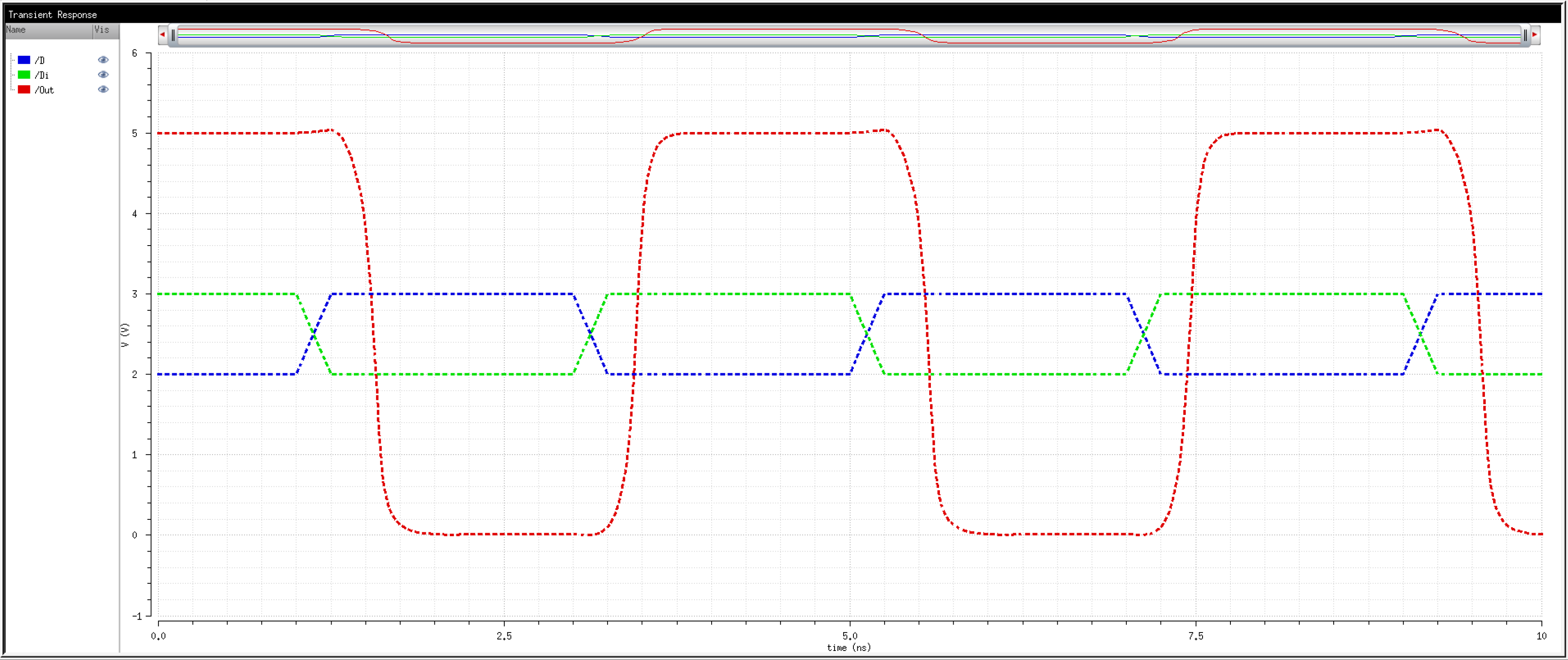
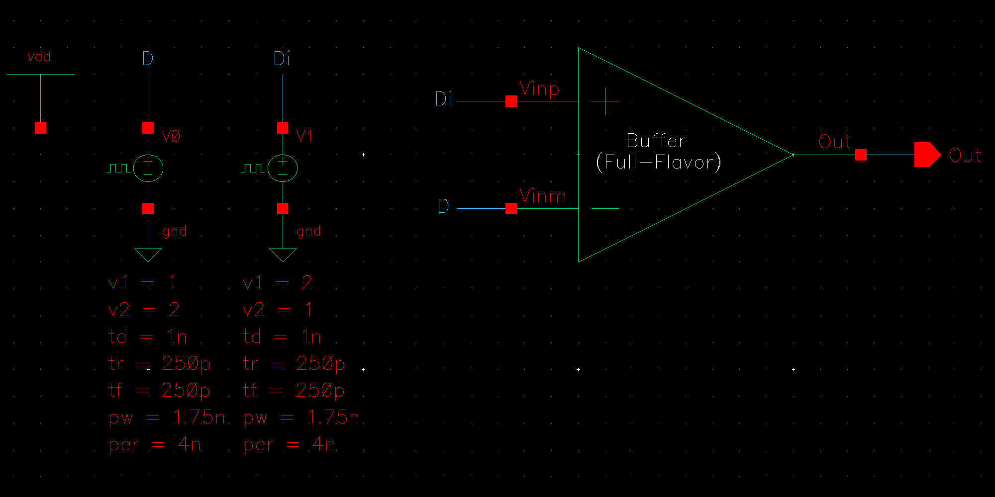
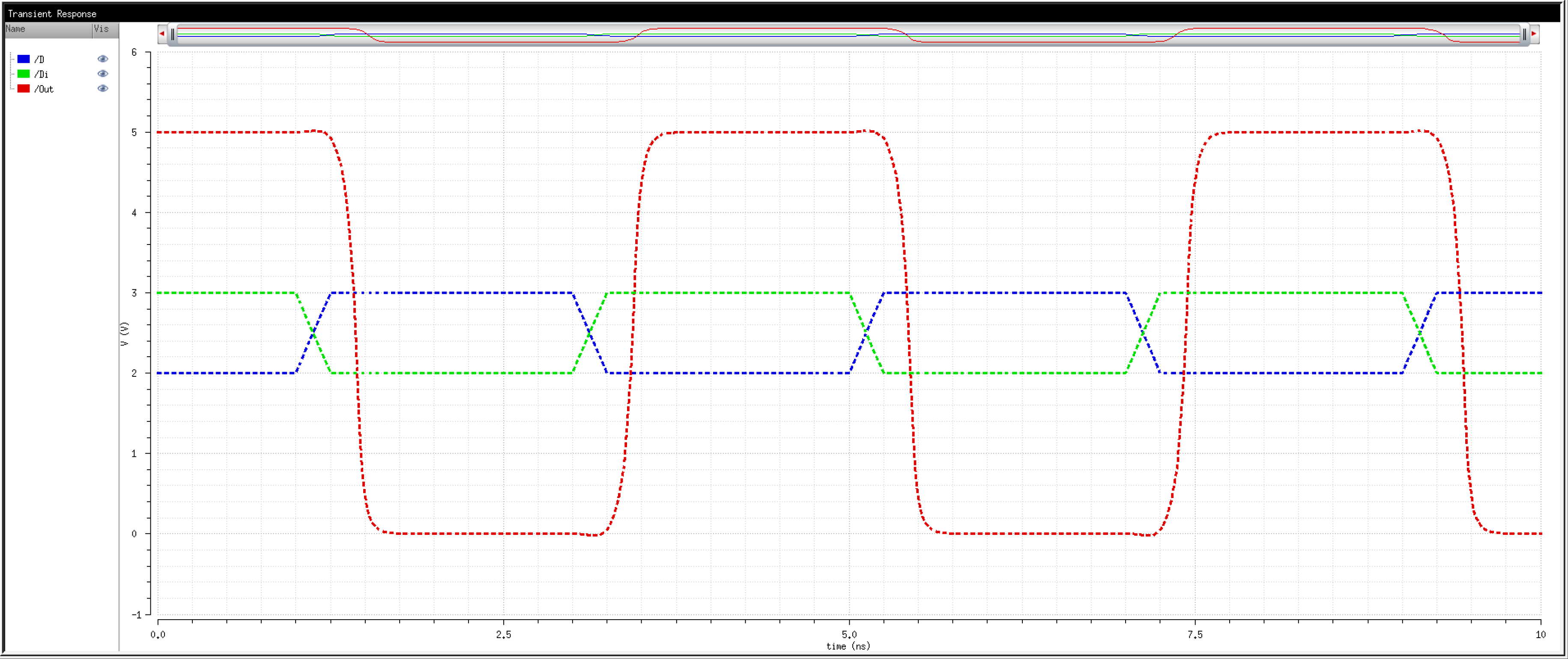
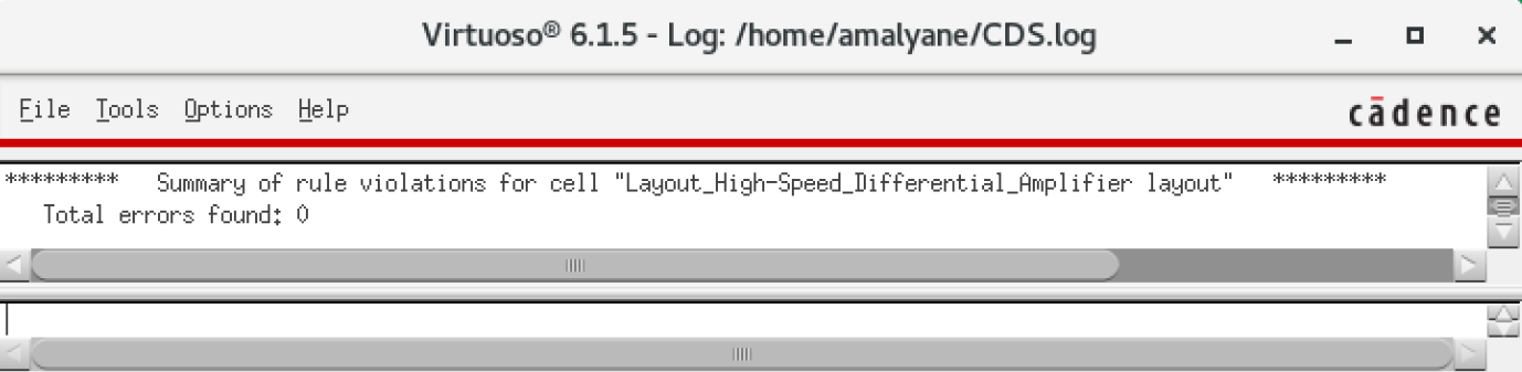
So, then, how fast can we operate the circuit? Let's try 2Gbps.

N_Flavor_2GBPS_sim_sch.png    N_Flavor_2GBPS_sim_plot.png

What is happening here? First of all, it takes a considerable amount of time for the buffer to reach steady state and for the output to actually become relatively stable. Second of all, the output is not 0 or 5V. Our amplifier is useless. If anything, it is more of an attenuator.

Just to quickly describe the simulation, D and Di are the differential inputs. Since we are talking about real world signals, the rise/fall times are not instant, so we must simulate this. 1/period as shown in the schematic would give us the frequency of the input. The output must correspond to and meet the timings of the inputs to avoid packet loss.

Let's try something a little slower.

N_Flavor_250Mbps_sim_sch.png    N_Flavor_250Mbps_sim_plot.png

We can analyze the operation:
When Di > D -> Out = 1

When Di < D -> Out = 0

This is the correct behavior.
We can see that the amplifier produces 0V for logic low and 5V for logic high. Our input buffer is now doing its job at a speed of 250Mbps.

Let's calculate the delays. We can create markers at appropriate locations or use the delay function in the calculator.

N_Flavor_250Mbps_sim_calc.png

First let us approximate the delay from a low to high transistion, or abbreviated to tPLH. The buffer switches the output state from a low to high when Di becomes greater than D. We send the signals Di and Out to the calculator and select the delay function in the panel. We put Signal1 as Di and Signal2 as Out. Di switches from 1V to 2V. We want the 50% point so we enter 1.5 as Threshhold Value 1. Next we want the 50% point of the output, so we enter 2.5 for Threshhold Value 2. Since we are after a low to high transition for both Di and Out, we specify both edge types as rising. The syntax for this function can be seen in the stack and below.

We get the following result after evaluating.

N_Flavor_250Mbps_sim_tplh.png

The parameters for the high to low transition, or tPHL, can be seen in the buffer, in the Function Panel, and below. The differences are that both edge types are now set to falling, and the edge number is set to 2, to skip the first falling edge occurence (so our result is more accurate and not affected by the 1ns startup delay we have set in the voltage sources).

N_Flavor_250Mbps_sim_tphl.png

Our results match what we would have calculated performing the operations manually.

Now let's try with a slightly more degraded signal. This can simulate a longer cable. Logic low is now 1.25 rather than 1V and logic high is now 1.75 rather than 2V.

N_Flavor_250Mbps_LV_sim_sch.png    N_Flavor_250Mbps_LV_sim_plot.png

N_Flavor_250Mbps_LV_sim_tplh.png

N_Flavor_250Mbps_LV_sim_tphl.png

We can see that both delays, especially tPLH, are considerably longer. This is to be expected as the difference between the signals was halved from 1V to 0.5V.

What if the difference between the two input signals stayed the same, say 1V as in the first example, but the voltage levels went up? Let's try D = 2V when Di = 3V.

N_Flavor_250Mbps_HV_sim_sch.png    N_Flavor_250Mbps_HV_sim_plot.png

N_Flavor_250Mbps_HV_sim_tplh.png

N_Flavor_250Mbps_HV_sim_tphl.png

We can see that both delays are now shorter. As mentioned, the magnitude of the difference between the signals is still 1V, but the delays are shorter from raising the voltage levels themselves. This would imply that the N-Flavor input buffer performs better with higher rather than lower voltage levels. Notice however that the voltage of logic high is ever so slightly worse now. Both of these phenomena can be explained by analyzing the regions that the MOSFETs are operating in. The MOSFETs move closer into the subtreshhold region when the inputs move closer to ground, in turn causing the propagation delays to increase and the output signal level to decrease. Perhaps we can avoid this by using a different design.

P-Flavor
A concise transistor level schematic of the P-Flavor input buffer is seen below (Figure 18.21).

P_Flavor_sch.png

NMOS are 6u/0.6u and PMOS are 12u/0.6u (as before).


P_Flavor_250Mbps_sim_sch.png    P_Flavor_250Mbps_sim_plot.png

P_Flavor_250Mbps_sim_tplh.png

P_Flavor_250Mbps_sim_tphl.png

We can see from the results that the P-Flavor input buffer has shorter delays with lower input voltage levels compared to the N-Flavor. Notice however that logic low has a positive offset. This occurs because the output changes at the same that Di passes D. Also note, for the sake of completeness, that we used 2.5V as the 50% point for the output, ignoring the fact that the 0.2V offset raises the 50% point to about 2.7V. If we were to evaluate the delay using a threshold of 2.7V, we would see that tPLH would increase to 246ps and tPHL would decrease to 376ps. The total delay, tPHL + tPLH, however, is hardly affected.

Let's try the higher input levels to further verify our results.

P_Flavor_250Mbps_HV_sim_sch.png    P_Flavor_250Mbps_HV_sim_plot.png

P_Flavor_250Mbps_HV_sim_tplh.png

P_Flavor_250Mbps_HV_sim_tphl.png

As expected, the P-Flavor is slower when the voltage levels increase, contrary to the N-Flavor.

As a final note for this section, it is important to point out that the performance of the P-Flavor using non-ideal voltage levels is actually very close to the performance of the N-Flavor when using ideal voltage levels. So one might conclude that the P-Flavor is preferred in all cases. This however cannot be stated as fact, as we have not simulated every possible combination of voltage levels or various types of loads. The take away from this section is that both the N and P flavors have their advantages and disadvantages, and neither one is superior in all scenarios.

The solution is obvious then, why not combine both flavors to create the ultimate differential amplifier? Well, that's exactly what we are going to do.

N-Flavor + P-Flavor = Full-Flavor
Here we create a rail-to-rail input buffer based on the previous two designs by putting them in parallel (Figure 18.23).

Full_Flavor_sch.png

Low Levels:
Full_Flavor_250Mbps_sim_sch.png    Full_Flavor_250Mbps_sim_plot.png

Full_Flavor_250Mbps_sim_tplh.png

Full_Flavor_250Mbps_sim_tphl.png

High Levels:
Full_Flavor_250Mbps_High_sim_sch.png    Full_Flavor_250Mbps_High_sim_plot.png

Full_Flavor_250Mbps_High_sim_tplh.png

Full_Flavor_250Mbps_High_sim_tphl.png

Now that we have simulated the various designs, we can summarize the performances.

Rising Edge Delays (tPLH)
DesignLow LevelsHigh Levels
N-Flavor614.2434.5
P-Flavor242.3330.8
Full-Flavor272.4307.9

Falling Edge Delays (tPHL)
DesignLow LevelsHigh Levels
N-Flavor503.4326.1
P-Flavor383.7434.2
Full-Flavor355.2305.4

From the data above, we see that the Full-Flavor design has the best performance in 3/4 tests. It is clearly the best design and will be the design in which we use from now on to design the most optimal version, in both speed and power consumption, of a differential amplfier.

Stress Testing
Now that we have combined the N-Flavor and P-Flavor, we have a robust Full-Flavor buffer that works over a wide range of operating voltages. Our design performs as expected regardless of relatively low or relatively high voltage levels.

Let us try and input some more challenging signals to test our new design. As previously mentioned, the differential amplifier amplifies the difference between two signals. As shown, if the difference is smaller, then the job of amplifier is more difficult and various performance metrics can suffer as a result.

How about we swing D and Di back and forth between 2.75 and 3V. The difference in voltage will now be 1/4th of what we have been testing so far. Can we still acheive a bit width of 4ns?

Full_Flavor_250Mbps_Harder_sim_sch.png    Full_Flavor_250Mbps_Harder_sim_plot.png

Full_Flavor_250Mbps_Harder_sim_tplh.png

Full_Flavor_250Mbps_Harder_sim_tphl.png

Our amplifier performs admirably. Remember that the signal is much smaller now and there is less to amplify. The N-Flavor or P-Flavor alone would have struggled.
We do notice however that we don't quite have full output logic levels. Logic low hovers about 100mV above 0 and logic high falls short of reaching 5V, at 4.77V.
So how do we improve our design? Well, we have just stated that the problem is that the amplifier doesn't have enough power to fully drive the output to 0 and 5V. This problem is typical, and one solution is of course adding another inverter on the output.

Full-Flavor + Flavor = Fuller-Flavor
We add an identical inverter in series.

Fuller_Flavor_sch.png

Resimulating:
Fuller_Flavor_sim_sch.png    Fuller_Flavor_sim_plot.png

Fuller_Flavor_sim_tplh.png

Fuller_Flavor_sim_tphl.png

Now the amplifier is stronger and can drive the output to fuller logic levels. But this came at a cost. The delays are now slightly higher. This is to be expected, as we added a series component. The signal must now propagate through the second inverter. This is contrary to adding a parallel component like when we combined the N-Flavor and P-Flavor, where the input goes through both at the same time, and is ultimately limited by the slower flavor. Take note that the added inverter inverts the logic on the output, so we need to modify our delay function, as now when Di goes low, the output goes high. We can change the edge triggers or just simply trigger on D (the complement) rather than Di to keep the other parameters in the delay function the same.

At this point, our design works well. We can add some component parameter modifications in the future if needed after we further characterize our design.

Power Consumption
Let's see how much power our amplifier requires to perform its job.

To analyze the power consumed, go into the Outputs menu, click Save All, and check the total field in the power signals sections. This will save the power data that will be used to analyze the power consumed. After this step, we can start the simulation. We can simulate for a longer time to give us a more accurate result when we average it out or integrate. Let's simulate for 1 microsecond. We can set the Accuracy Defaults to conservative for a slower but more accurate simulation. After the simulation is complete, we can go into Results -> Direct Plot -> Main Form. We select transient analysis, Power under the Function field, and click Plot.

We can zoom in towards the end for a more precise visualization.

Fuller_Flavor_sim_power.png

Now we can use the average function in the calculator to give us the average power consumed by our amplifier. This is just the average value of the spikes.

Fuller_Flavor_sim_avg_power.png

While 10mV seems high, we have to remember that these are very fast burts, each lasting only nanoseconds. To get the total energy, we would integrate. We will perform this later on.

Loads
Up to this point, we have been testing our design using no load on the output. For our initial design choices this was fine, but to further optimize and characterize our design, we should simulate the buffer actually driving something.

Let's add a resistive load.

Fuller_Adder_res_sim_sch.png

We can simulate multiple loads in one simulation using parametric analysis. Note that we can just set the Run Mode to Parametric Set to only run our desired values (and avoid filling out redundant parameters).

Fuller_Adder_res_parametric.png    Fuller_Adder_res_parametric_plot.png

The lowest resistance (biggest load) will have the worst tPLH, and the highest resistance (smallest load) will have the worst tPHL. Let's calculate tPLH of the 1k load.

Fuller_Adder_res_parametric_tplh.png

Our design performs well.

Let us try a different type of load.


Fuller_Adder_cap_sim_sch.png

Fuller_Adder_cap_parametric.png    Fuller_Adder_cap_parametric_plot.png

Fuller_Adder_cap_parametric_tphl.png

The delay is high with the 1pF load. With the other three, the worst delay is tPHL of the 100fF load at 800ps. This is still acceptable.

Further Analysis
At this point, if we required faster edges, we could change the sizes of the MOSFETs in our schematic. Remember, however, that the maximum speed is ultimately limited by the process we use, which is C5 in our case. My MOSFETs are already at the minimum length of 600nm. Essentially, the smaller the process, then the smaller the transistor possible in that process, so the faster the process. The top PMOS in the N-Flavor and the bottom NMOS in the N-Flavor have a great impact on the signal path. If we were to start changing the sizes of the transistors, then these two would be the place to start. However, I quite like the sub 10mW average power consumption of my design. Increasing the edge speeds would mean greater power consumption. This is because Average Power is a function of frequency.

Below we see the buffer operating at 2x the frequency. The average spike is slightly higher, but they occur 2x more often, causing an increase in power consumption.


Fuller_Flavor_sim_power_fast.png

Integrating would give us the total energy consumed.

Fuller_Flavor_sim_integ_power_fast.png

Furthermore, an increase in power consumption will cause an increase in temperature.

To see this, let's simulate our design operating at different temperatures. I will use our current design with a 100fF capacitor on the output. Note that this load type and value is ideal because it's not too heavy of a load to cause the output voltage to drop
significantly, but also not too weak, as it does indeed stress the buffer and slow down the edges. This 100fF load is the green wave in the capacitive load plot above.

Fuller_Adder_temp_parametric.png

Fuller_Adder_temp_parametric_tphl.png

We can see a considerable increase in the delays as the temperatures goes up. A rise in temperatures can be relieved by putting a heatsink on our chip, but this would add to the cost of our design and increase the footprint.

To summarize, we see diminishing returns as we increase the speed, as it increases the power, which increases the temperature, which then decreases the speed.


Finding Limits
Now that we have characterized our design in a general way, let's try and find the extremes in which our design can function at.

We have shown thus far that our design, with an input differential of 250mV, can achieve 250Mbits/s with fast edges and low power consumption. What if there is even more loss in the cable? Let's try a differential of 125mV. Once again, I use the 100pF load on the output.

Fuller_Adder_125mV_sim_sch.png    Fuller_Adder_125mV_sim_plot.png

Fuller_Adder_125mV_sim_tplh.png

Fuller_Adder_125mV_sim_tphl.png

As mentioned, the lower the differential in the signal, the harder it is for the amplifier to actually amplify. This is why we see the edges slow down. However, the delay is still under 1ns which is what I am aiming for. Our design performs well even for small signals.

Now let's go the other direction. What if leave the signal differential to 250mV but try to run our design at a higher speed, such as 500Mbps?

Fuller_Adder_250Mbps_sim_sch.png    Fuller_Adder_500Mbps_sim_plot.png

The output waveform is not as square anymore. It is starting to look like a sine wave. Our edges are not ideal. However, just like above, our design could work if the component the amplifier is driving can tolerate such an input.

Finally, let's see how low VDD can go before our amplifier stops functionting. This is useful to know because we cannot control the VDD supplied to our amplifier after we ship it to the customer; it is whatever the circuit that the amplifier is used in can provide to it. It might be a stable 5V, it might not.

Fuller_Adder_vdd_sim_sch.png    Fuller_Adder_250Mbps_vdd_sim_plot.png

We can see that at 3V, the output is basically a line. At 3.1V, it starts to take shape. At 3.2, the output is better, but still not usable (take a look at the falling edge logic). At 3.7, the rise time is ideal, but the falling edge could be better. Past 3.7V we get diminishing returns in terms of the quality of the rising edge. I would consider this the minimum voltage for the circuit to function at. As we get closer to 4V, the circuit behaves as designed. At a VDD of around 4.3V, the circuit performs very well. Note that we do not specifically consider the performance of the output high voltage level itself because it is limited by VDD.


This concludes the design and characterization of our differential amplifier. Next we will perform the layout.


Layout:

It's a good idea to split our Fuller-Flavor schematic into multiple parts so we can divide and conquer. If we dive in head-first and just try to do the entire layout at once, then troubleshooting will be more difficult.

I have already drawn the three different parts of the differential amplifier: P-Flavor Input Buffer, N-Flavor Input Buffer, and Inverters.

Let's start with the most simple part.

Inverters
inverters_sch.png

inverters_layout.png    inverters_drc.png

inverters_extracted.png    inverters_lvs.png

N-Flavor Input Buffer
My goal for this layout was to acheive a balance between readability and performance.
I tried to make my layout match the general look of my schematic. This is not ideal if we were going to be selling our chips, but better for education purposes.
On the other hand, I made my layers wide and not thin like the wires in the schematic for better contact and resistance.

Layout_N_Flavor_sch.png

Layout_N_Flavor_layout.png    N_Flavor_drc.png

Layout_N_Flavor_extracted.png    N_Flavor_lvs.png

P-Flavor Input Buffer
Next we can layout the P-Flavor Input Buffer.

Layout_P_Flavor_sch.png

Layout_P_Flavor_layout.png    P_Flavor_drc.png

Layout_P_Flavor_extracted.png    P_Flavor_lvs.png

High-Speed Differential Amplifier
Finally, we perform the layout of the Fuller-Flavor schematic.

Fuller_Flavor_sch.png

Layout_Fuller_Flavor_layout.png    Layout_Fuller_Flavor_drc.png

Layout_Fuller_Flavor_extracted.png    Layout_Fuller_Flavor_lvs.png

Extracted Simulation
As a final verification, we can simulate our extracted view to make sure it surpasses the 250mV 250Mbps benchmark.

Sim_Layout_Full_Flavor_extracted.png

Sim_Layout_Full_Flavor_env.png

Sim_Layout_Full_Flavor_netlist.png

Sim_Layout_Full_Flavor_plot.png


Return to EE 421L Labs