Lab 7 - EE 421L
Author: Edgar Amalyan
Email: amalyane@unlv.nevada.edu
Date: 11/04/2020
Goals:
In
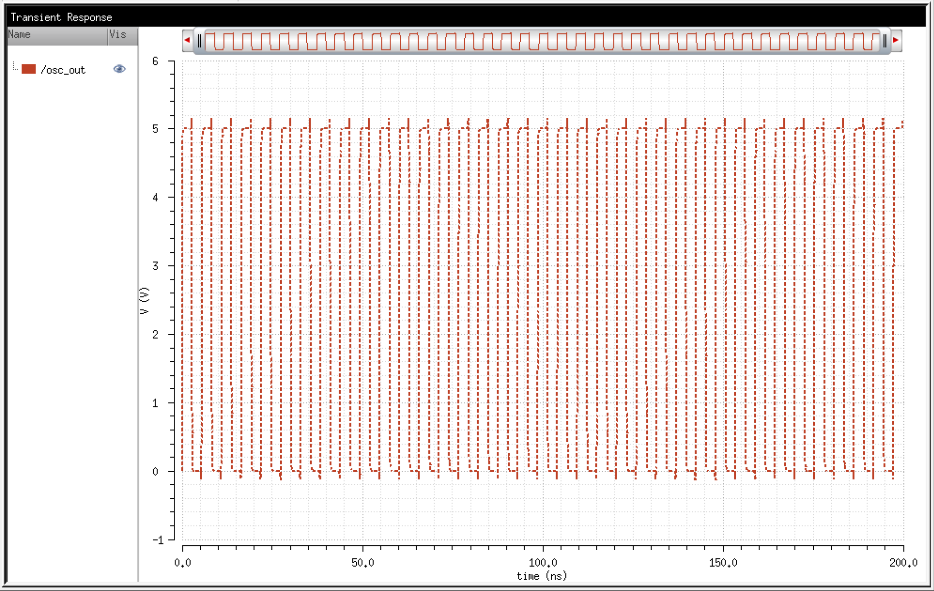
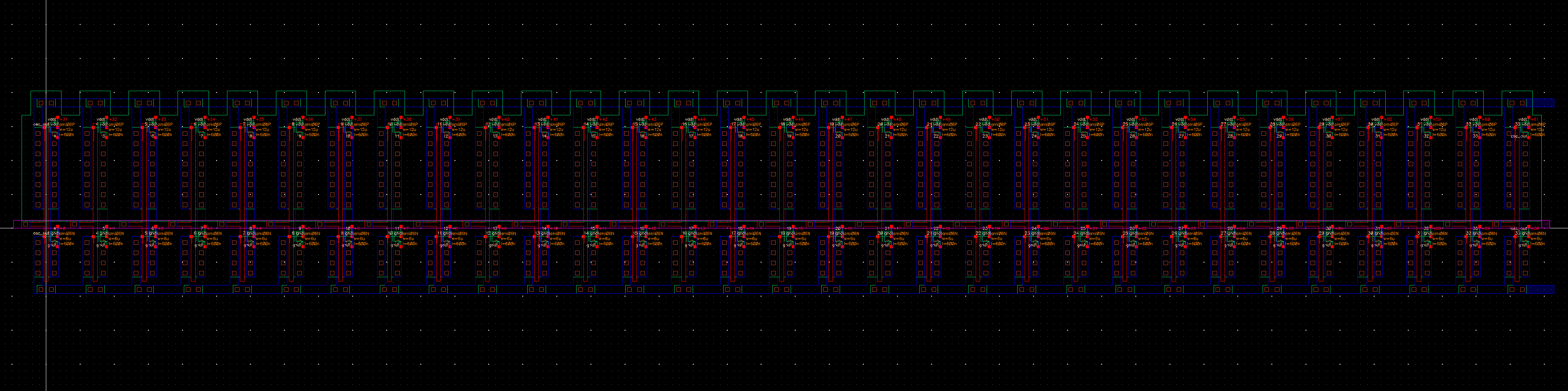
this lab, we will design, layout, and simulate a ring oscillator,
various logic gates, a multiplexer/demultiplexer, and a full-adder.
They will be constructed from 1-bit versions which will be used to build 8-bit array versions.
These components can then be used to build an ALU.
Prelab
Note:
Everything is a different aspect ratio, so I just made them all
relatively square so the page can be less of an eye-sore. Please click
on pictures for larger and less funky views. Tutorial 5
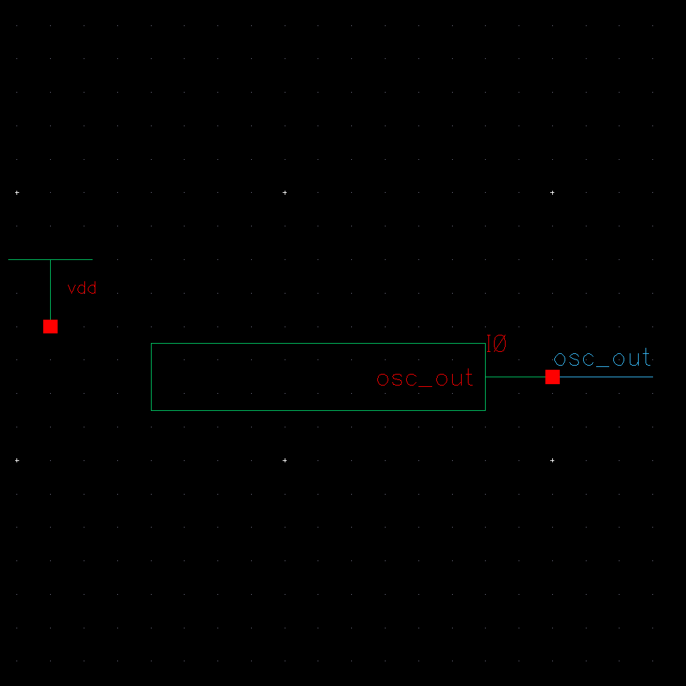
Schematic
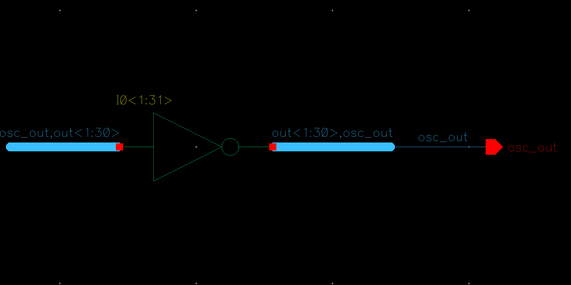
Simulation (using Symbol)
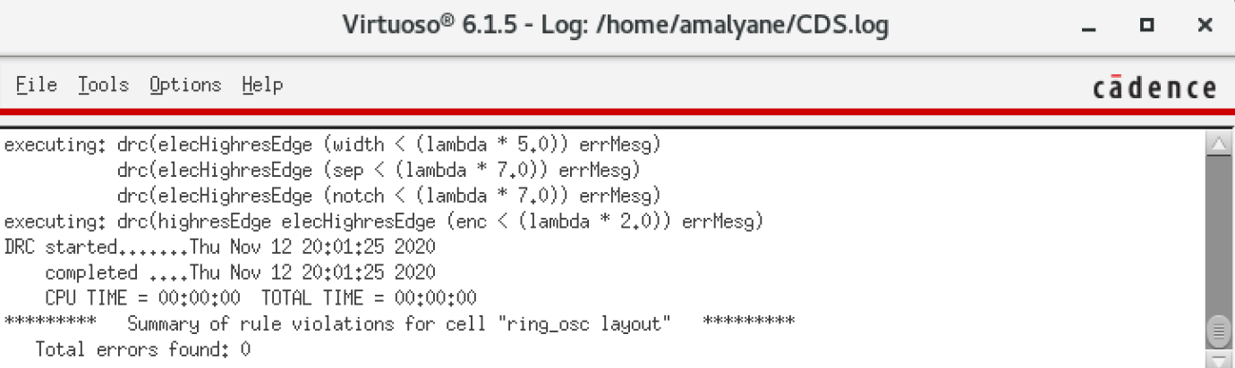
Layout and DRC
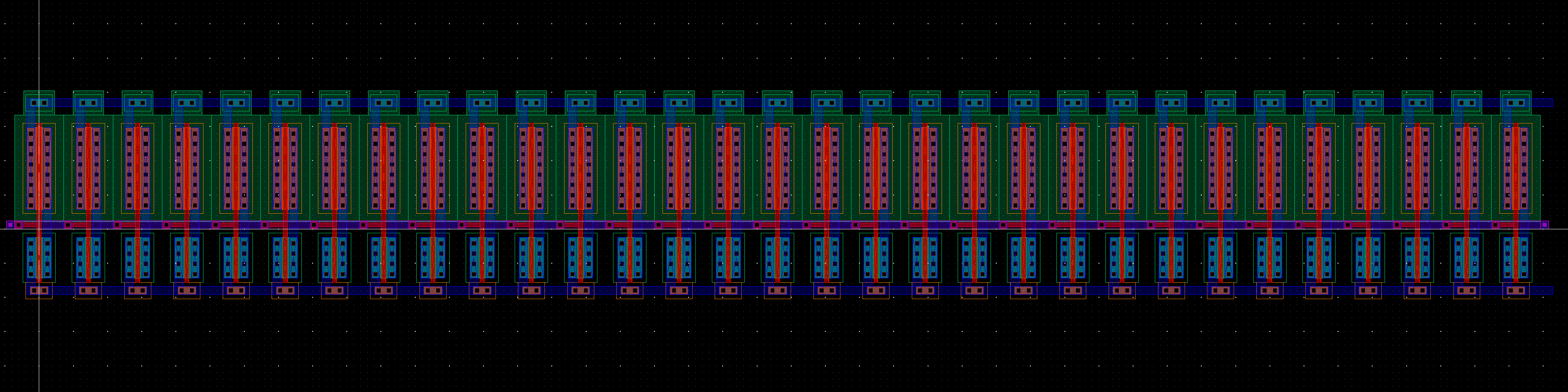
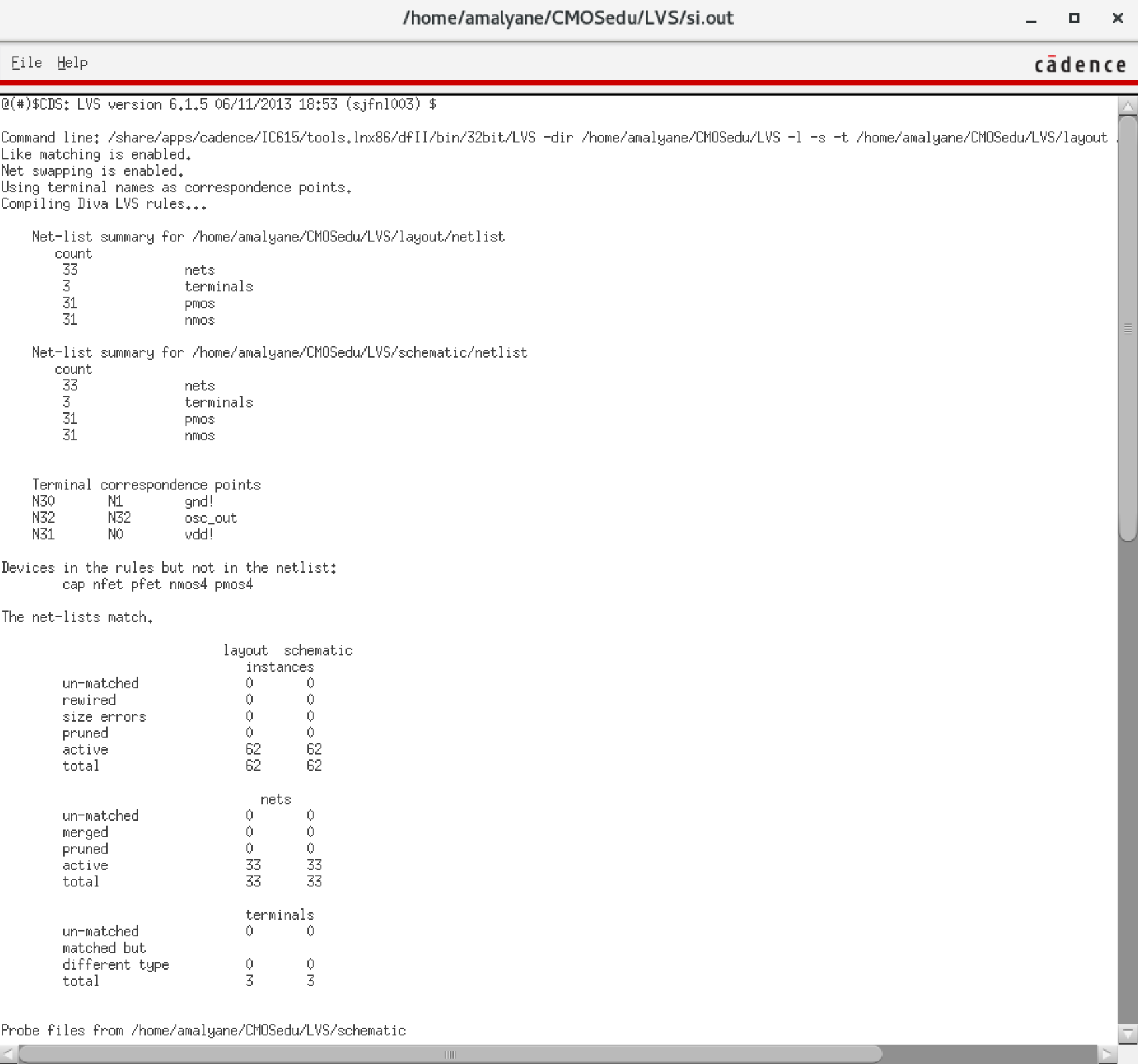
Extraction and LVS
Lab
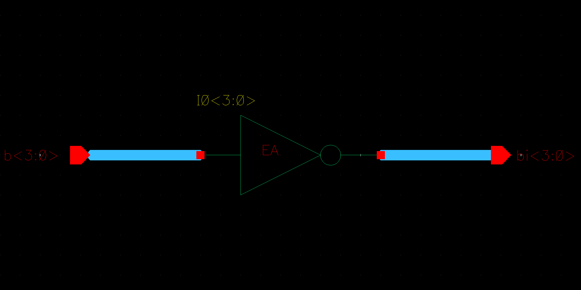
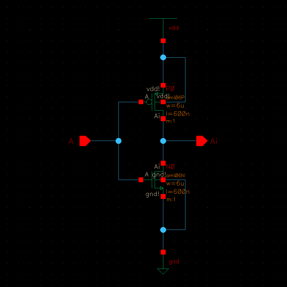
4-bit Inverter
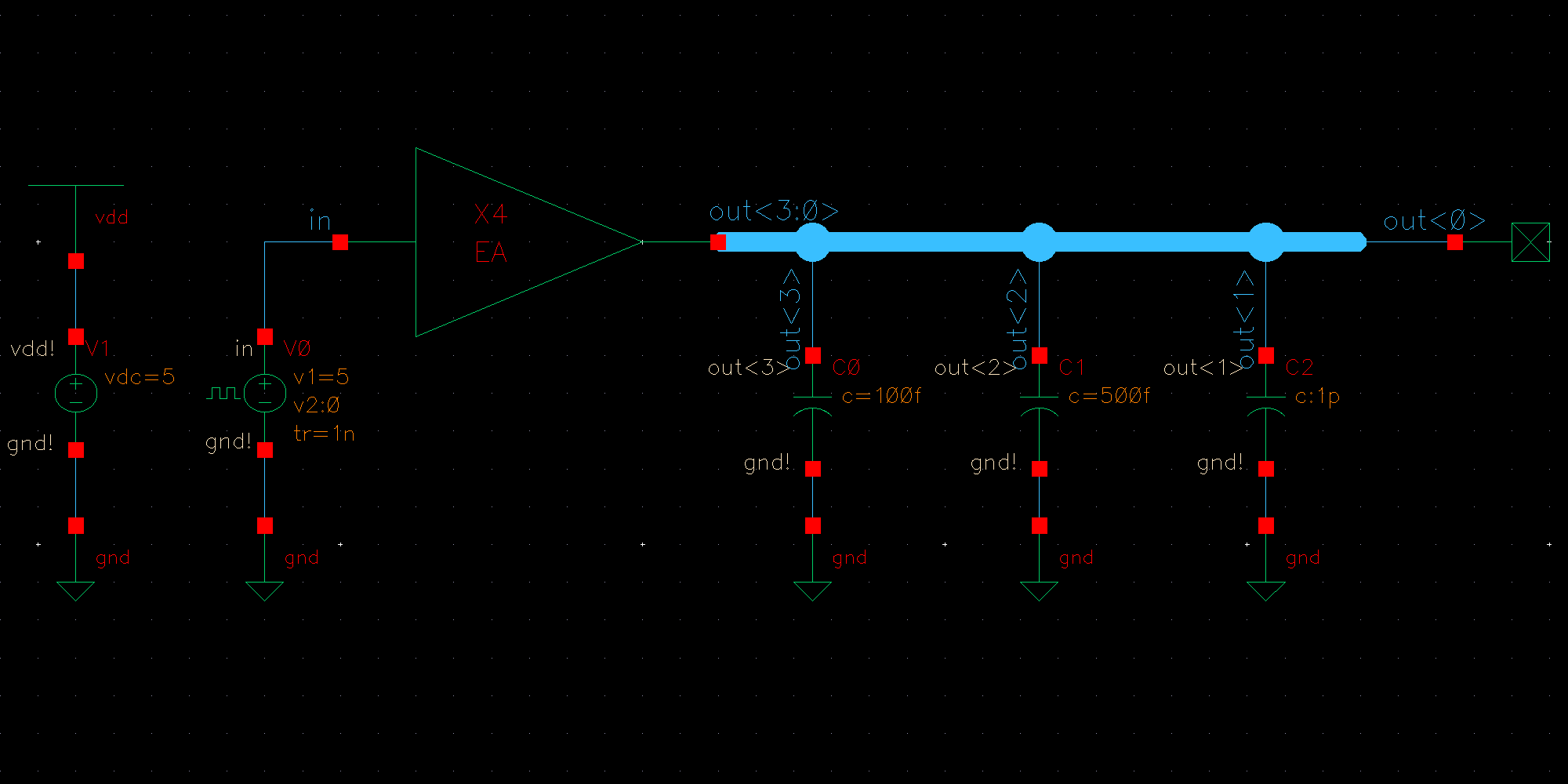
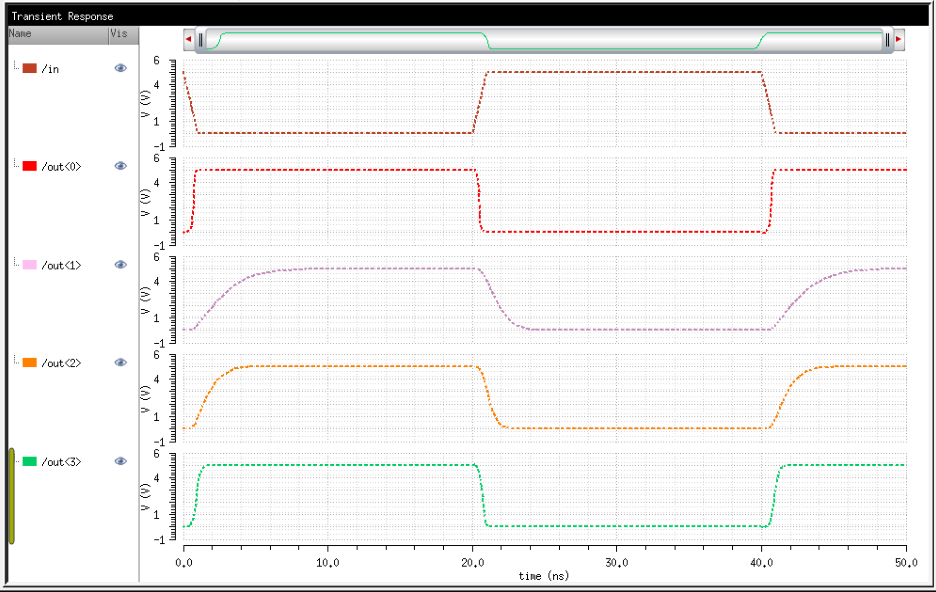
The
capacitors smooth the output. The larger the capacitor, the more energy
it has to be used when needed. But it also means more time to charge
and discharge, increasing the rise/fall times.
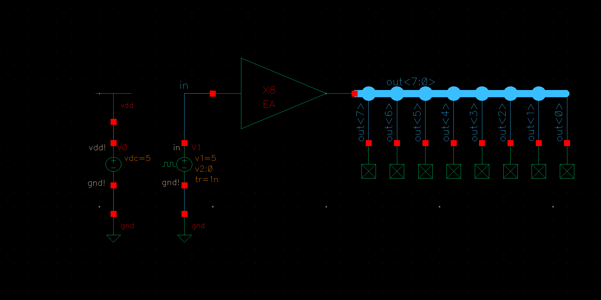
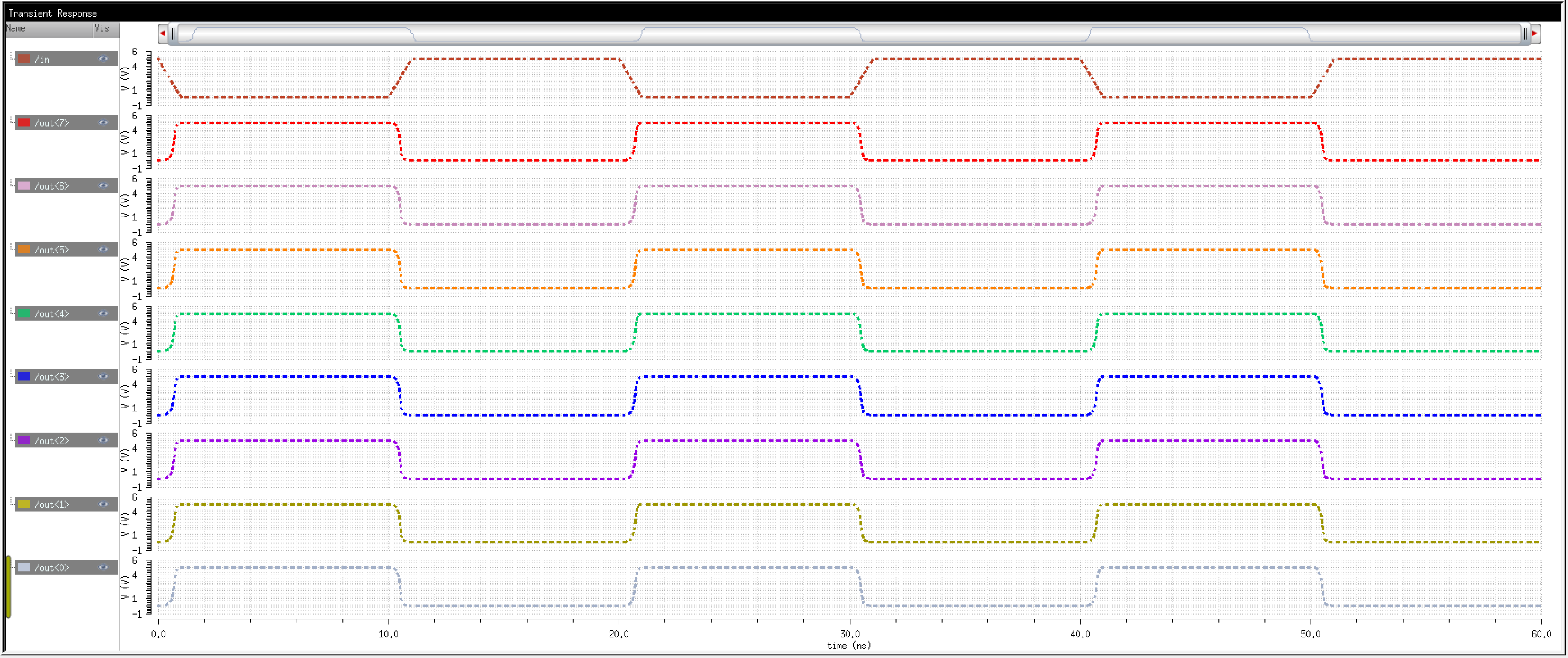
8-bit Array Inverter
For the simulations, we can plot all 8 elements of the array to make sure the connections are correct.
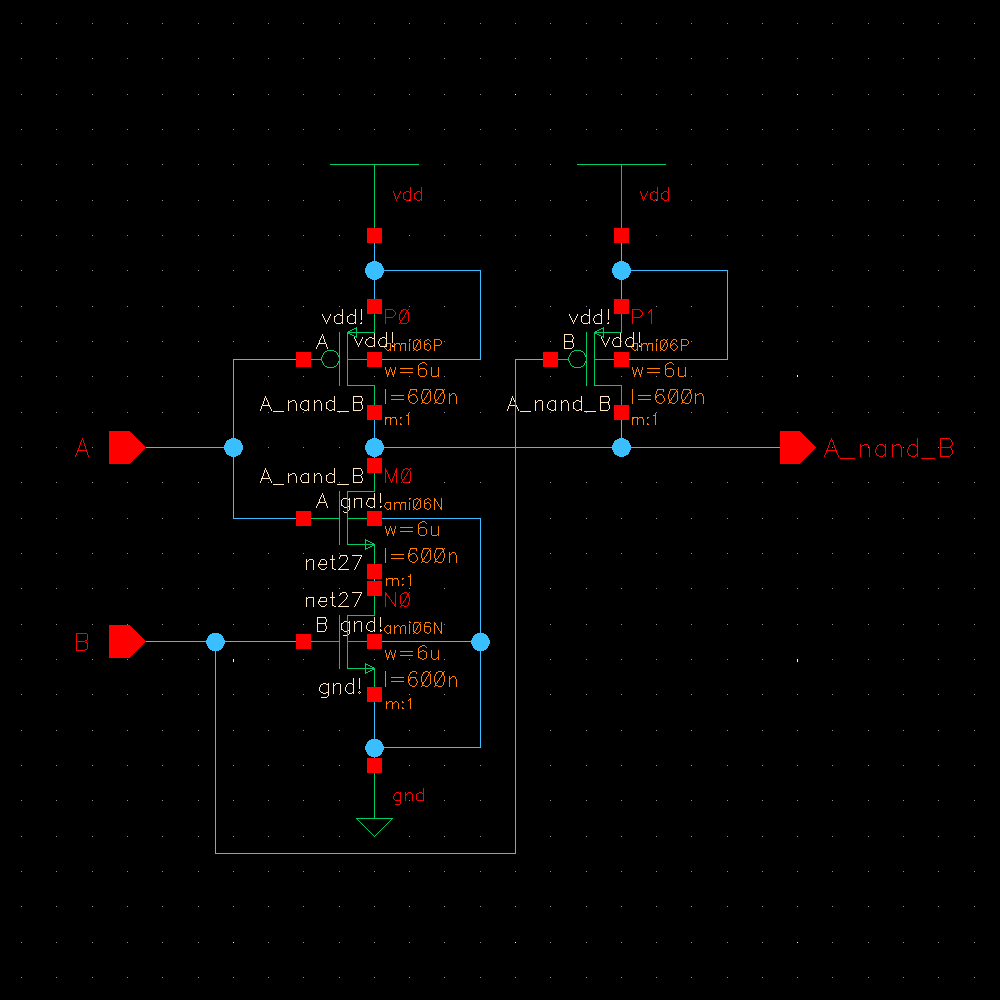
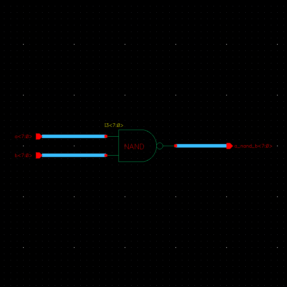
8-bit Array NAND
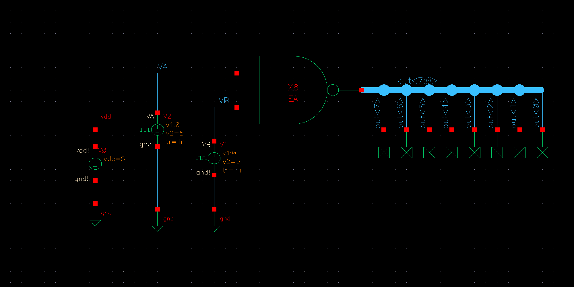
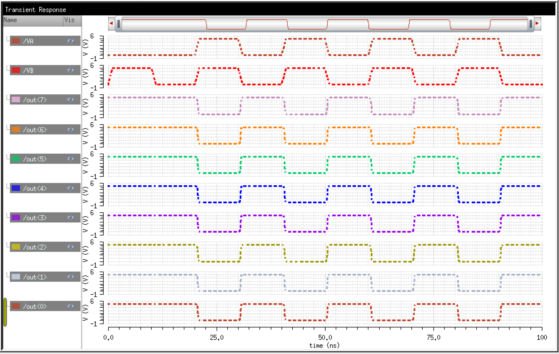
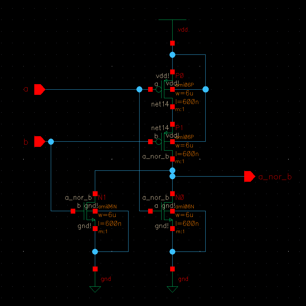
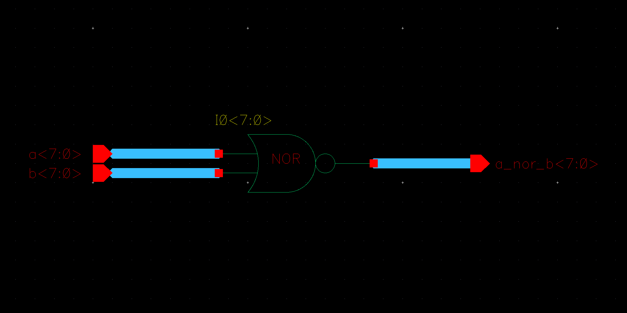
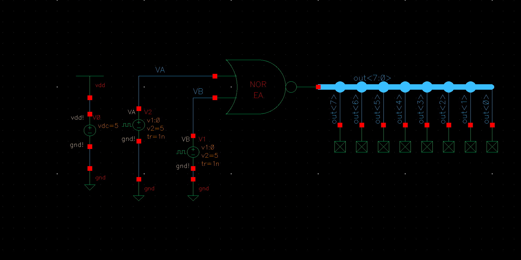
8-bit Array NOR

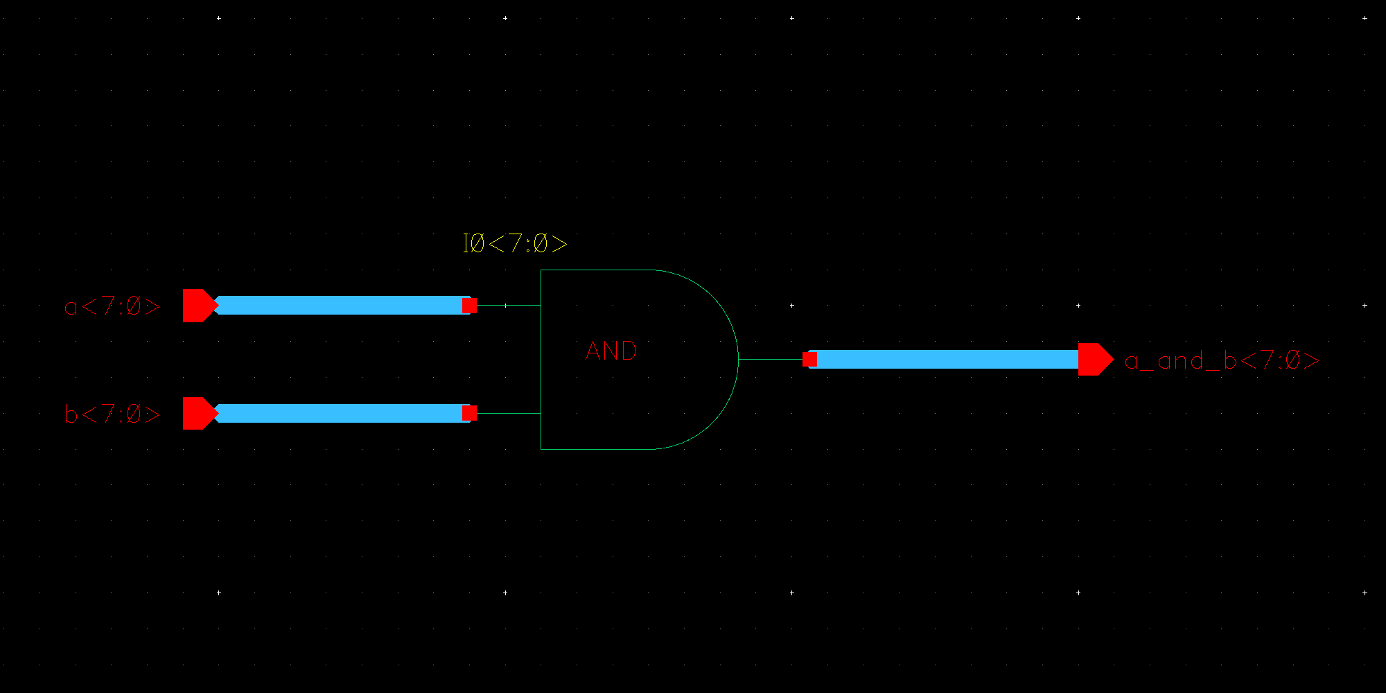
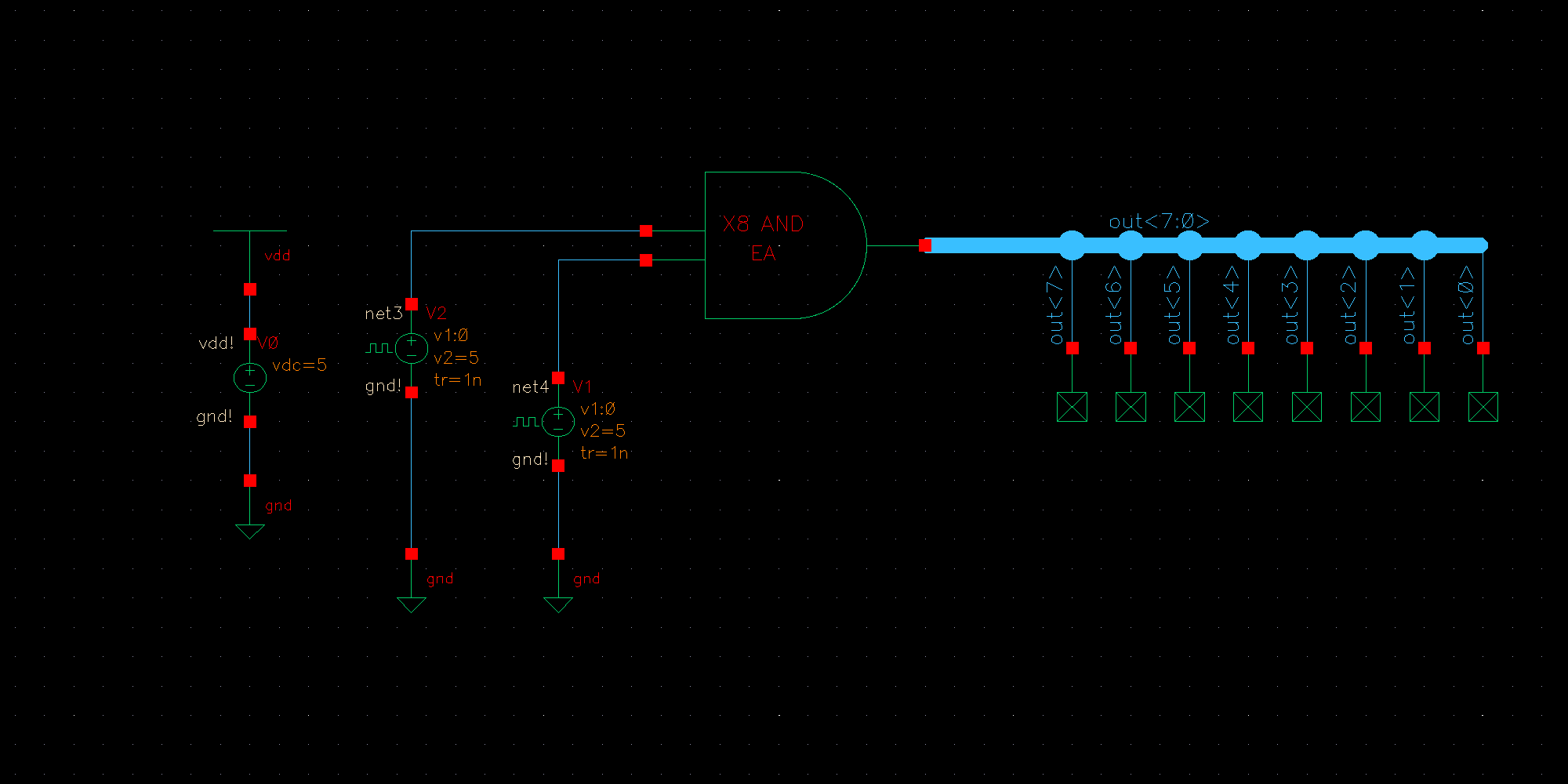
8-bit Array AND
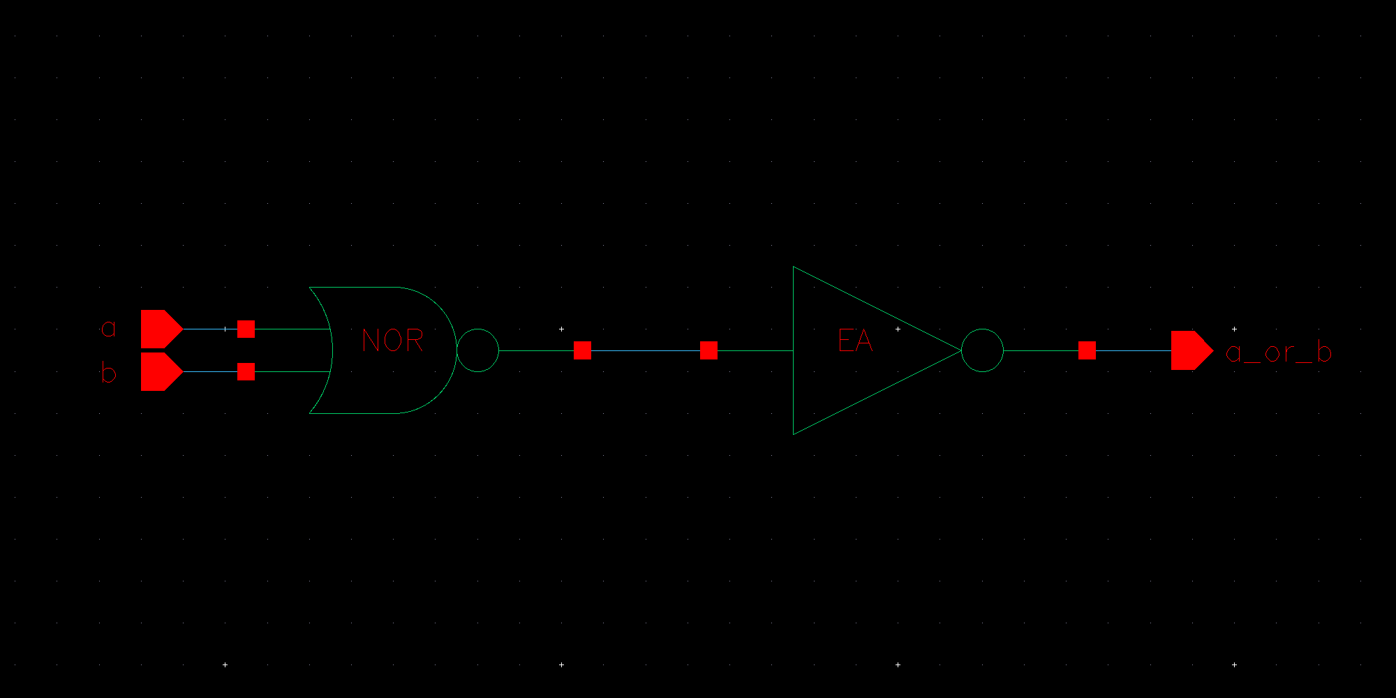
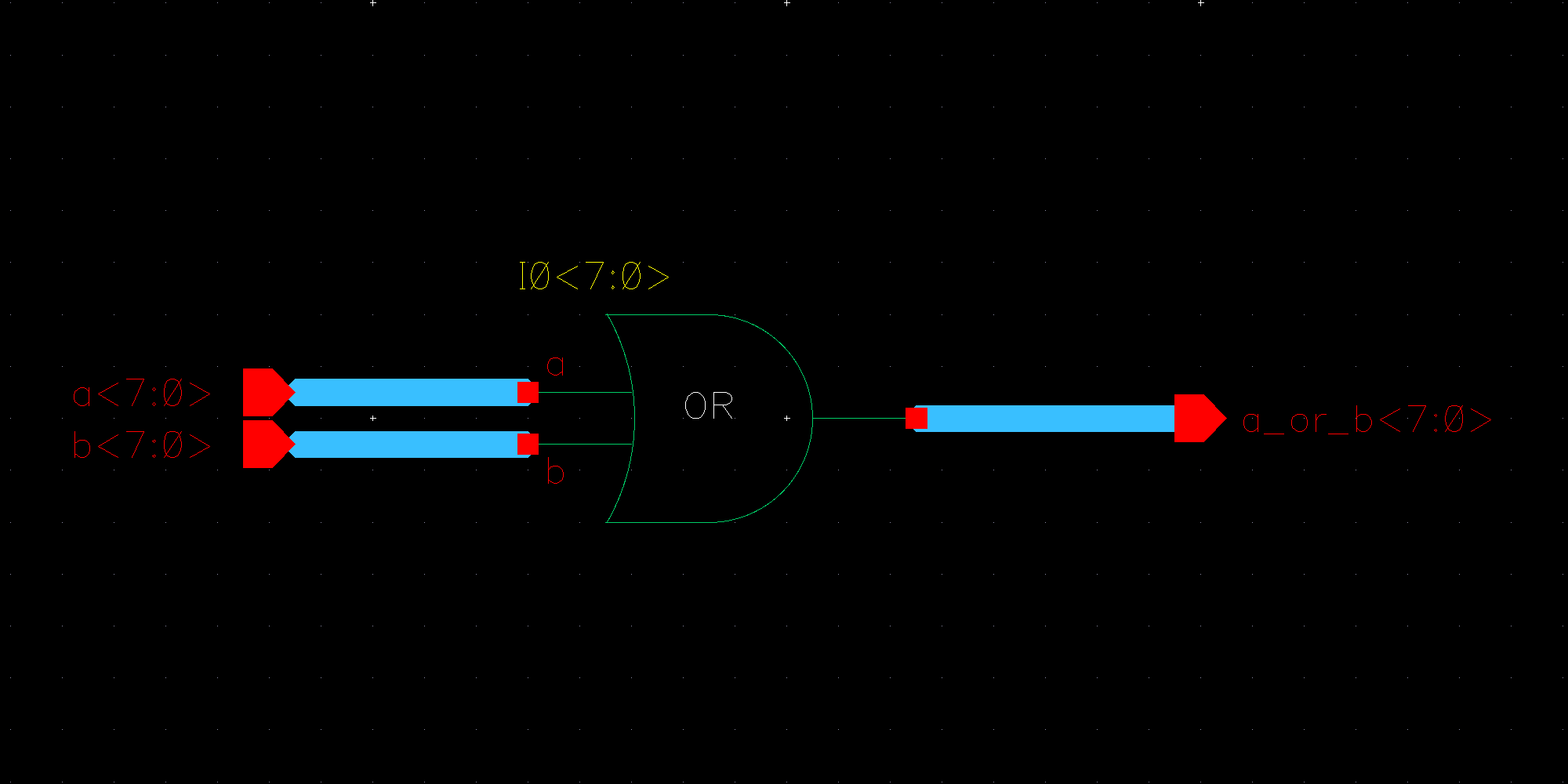
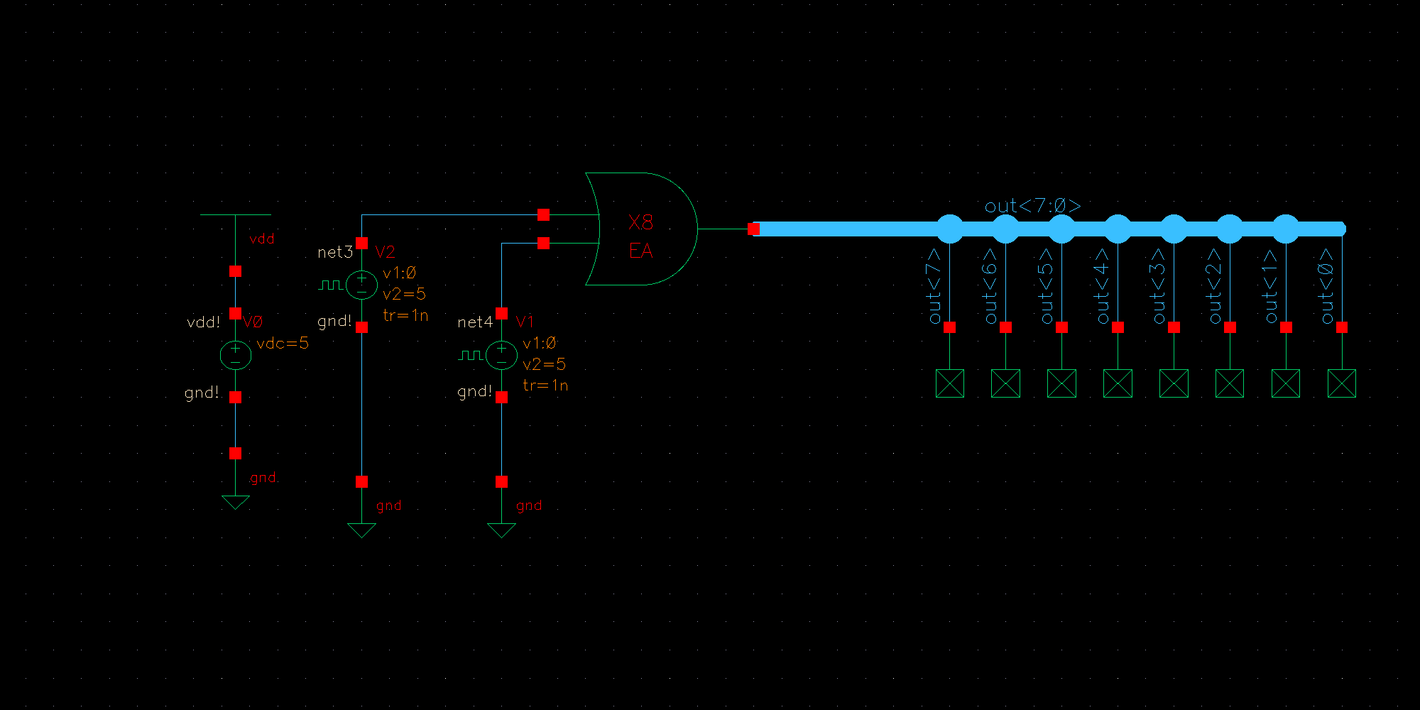
8-bit Array OR
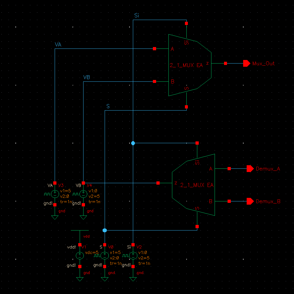
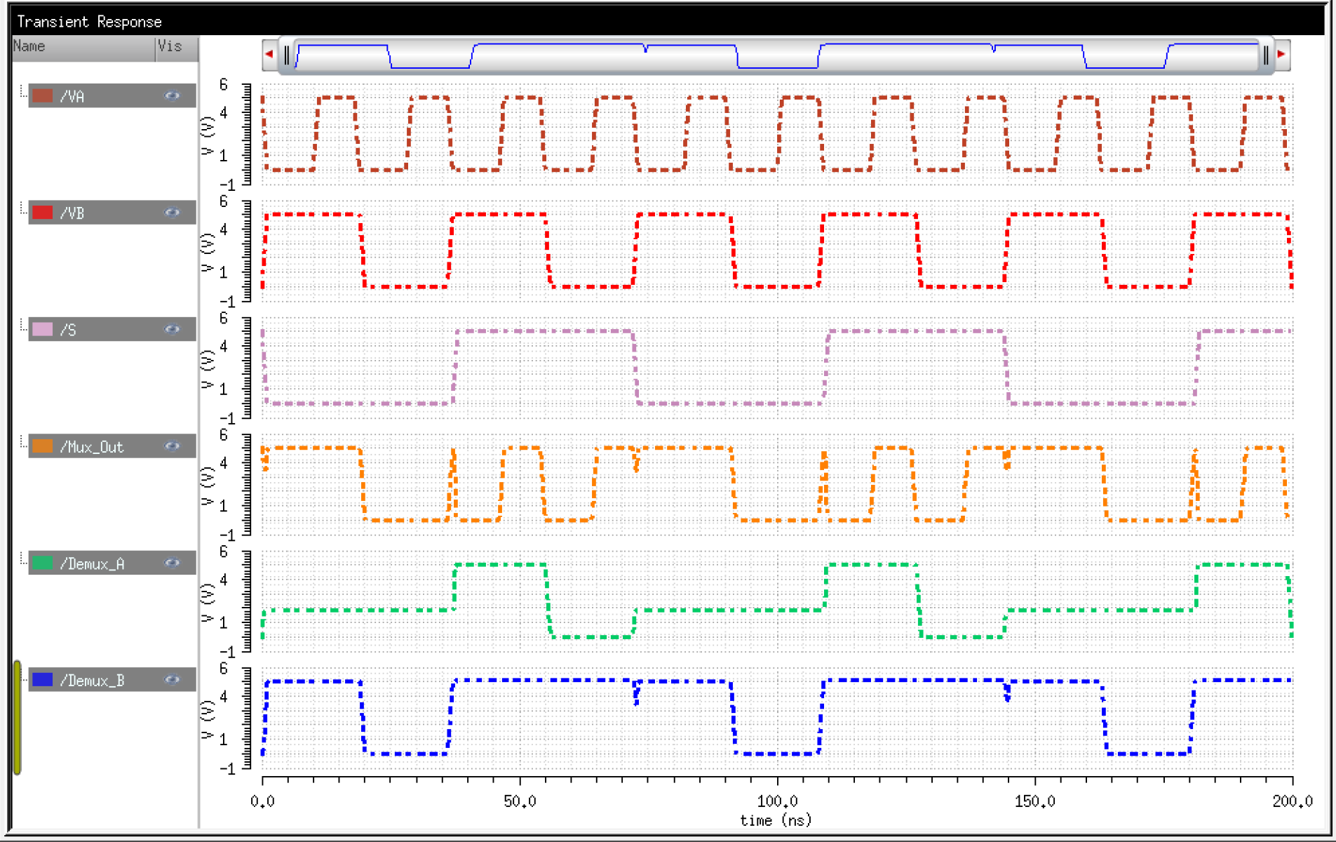
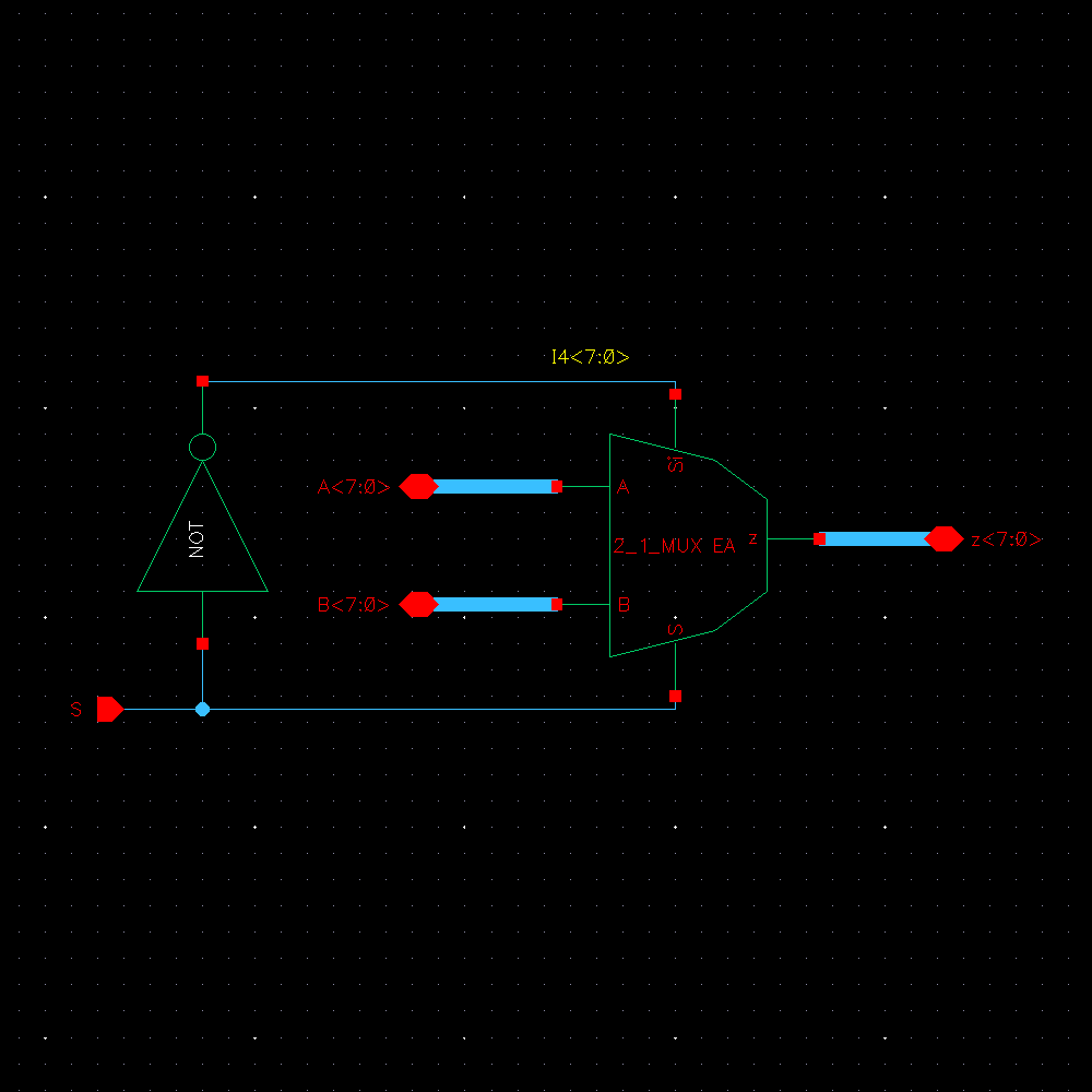
2-to-1 MUX
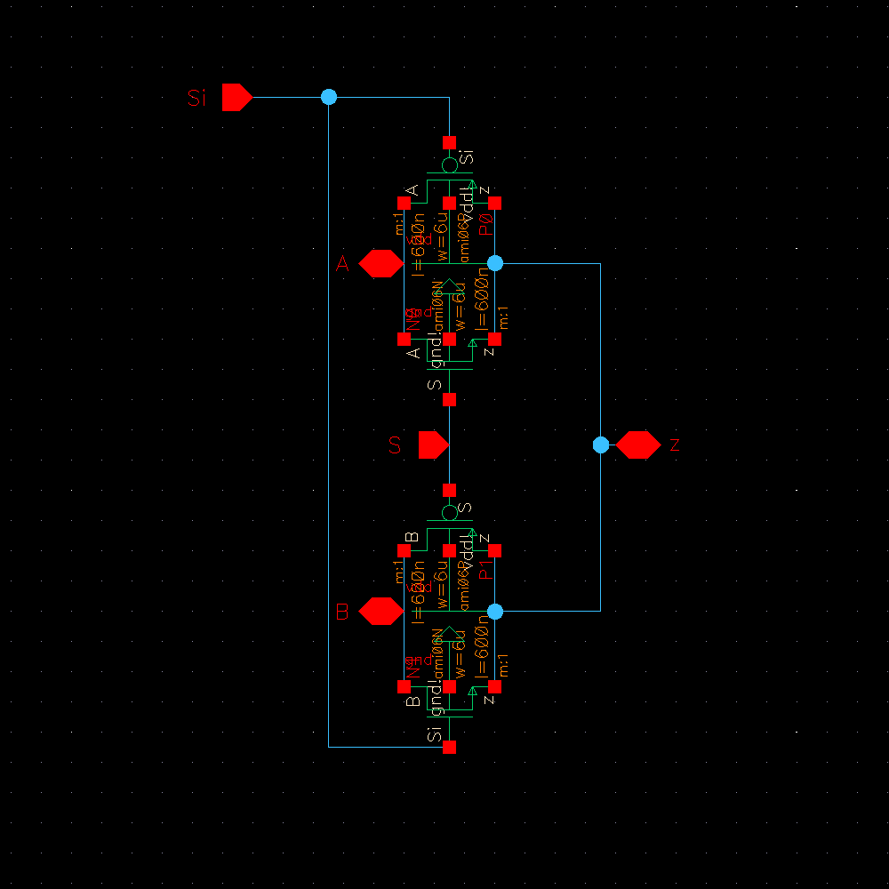
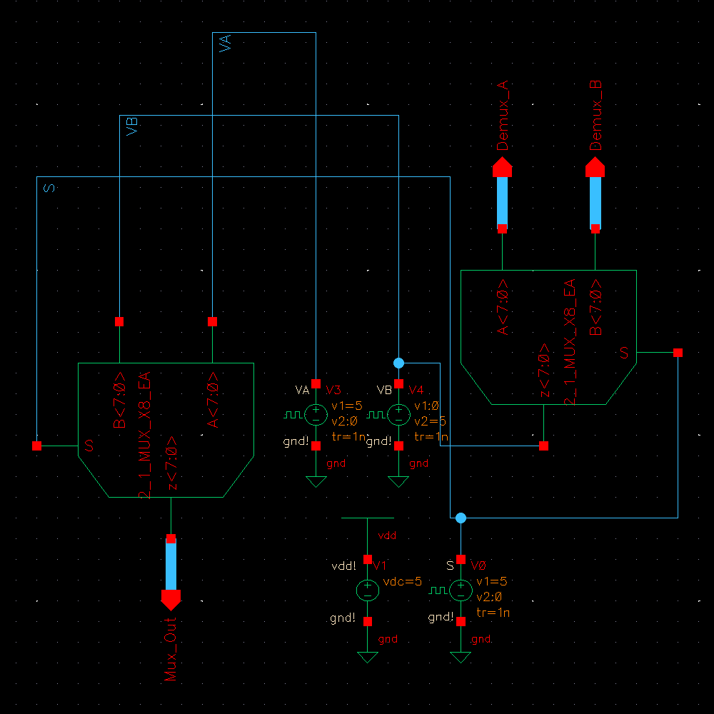
We can simulate both the MUX and DEMUX together by just reversing their inputs/outputs.
As can be seen below:
S = 1 => Out = A
Si = 1 => Out = B
and of course the reverse for the DEMUX.
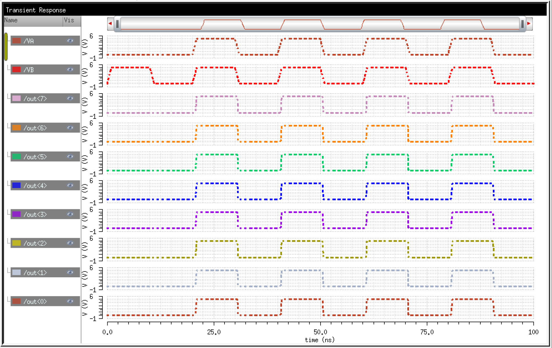
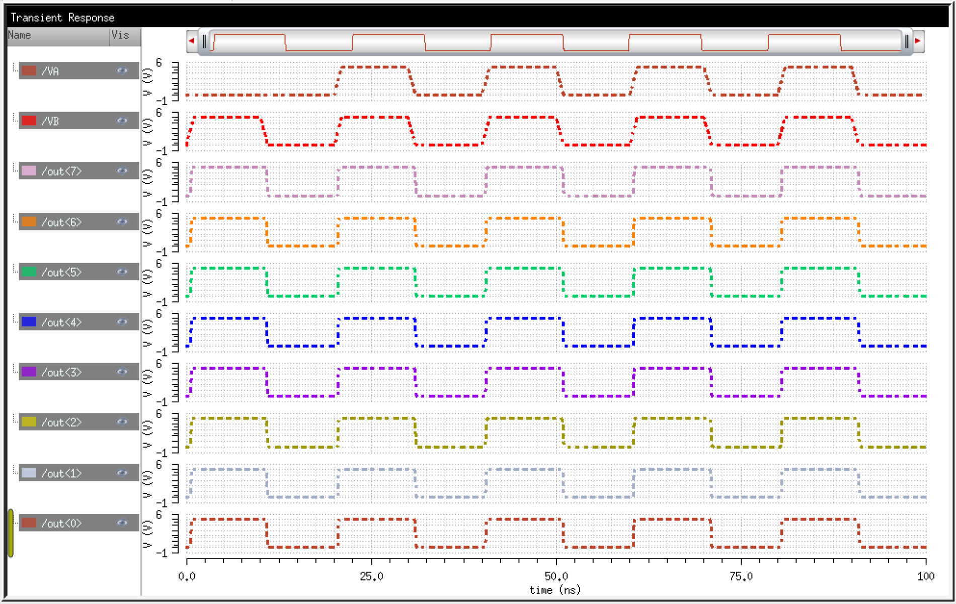
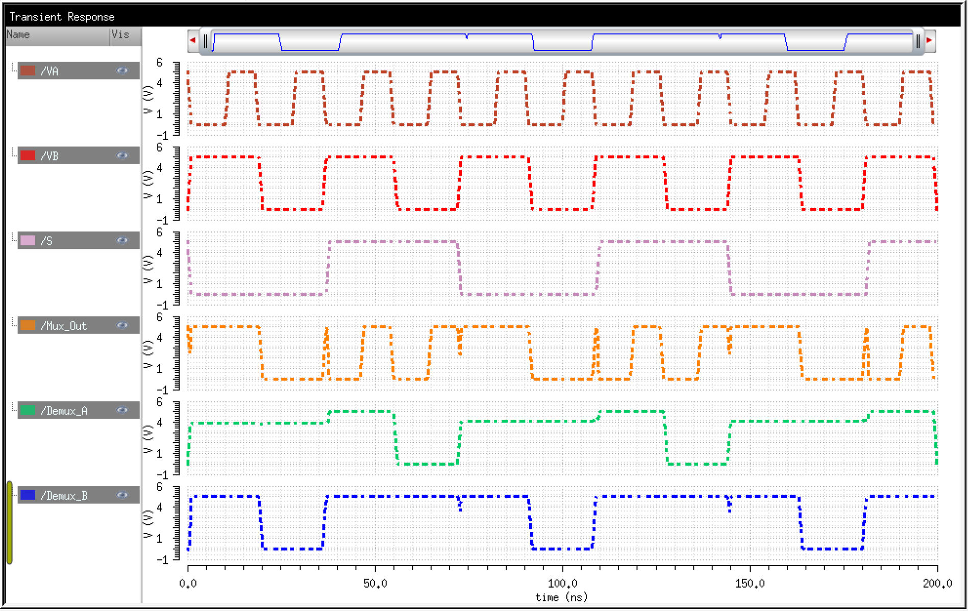
2-to-1 8-bit MUX
We
can note that the middle logic levels are due to transistions occuring
at the same time. The timings must be set appropriately.
As seen below:
S = 1 => Out = A
Si = 0 => Out = B
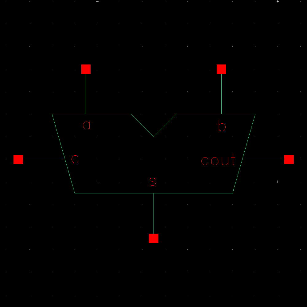
1-bit Full-Adder
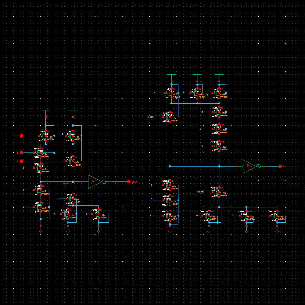
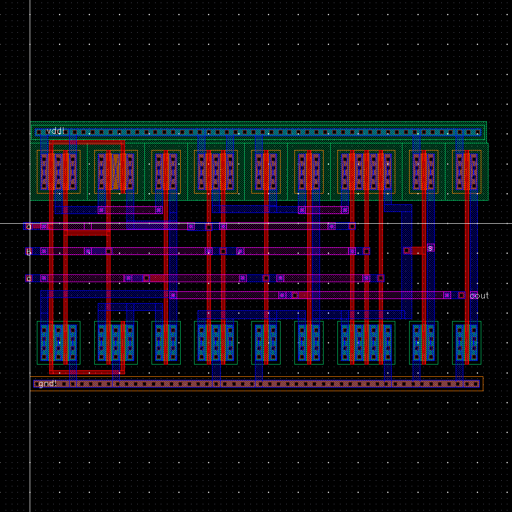
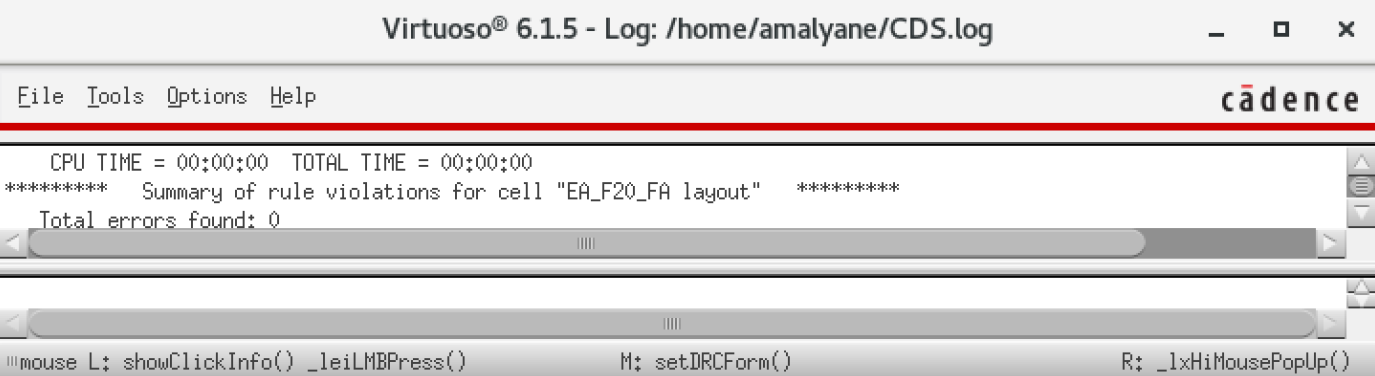
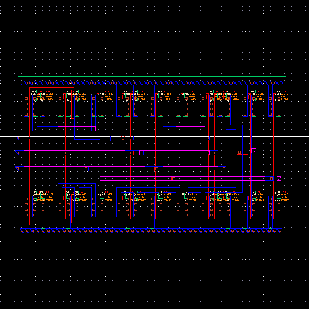
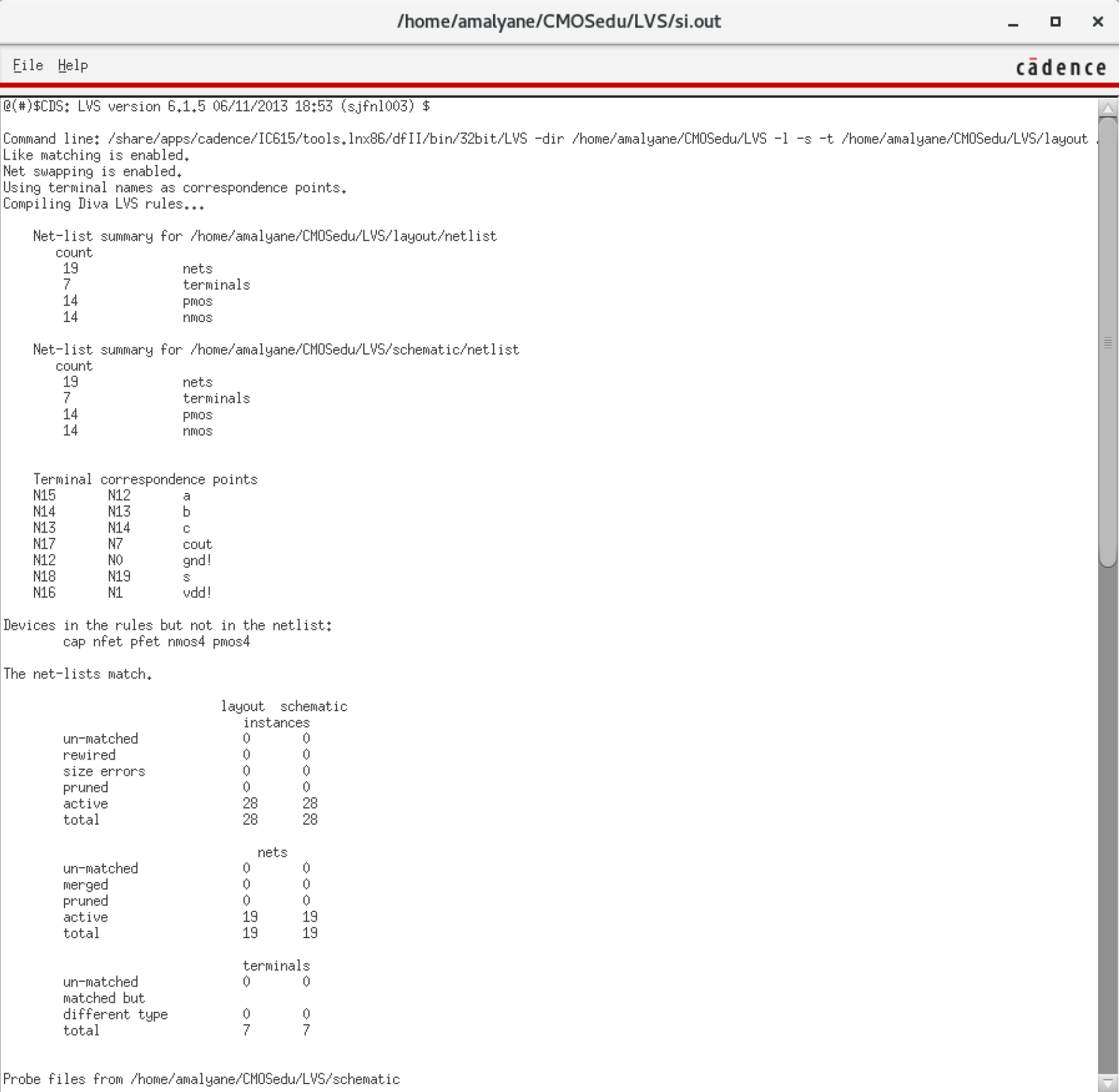
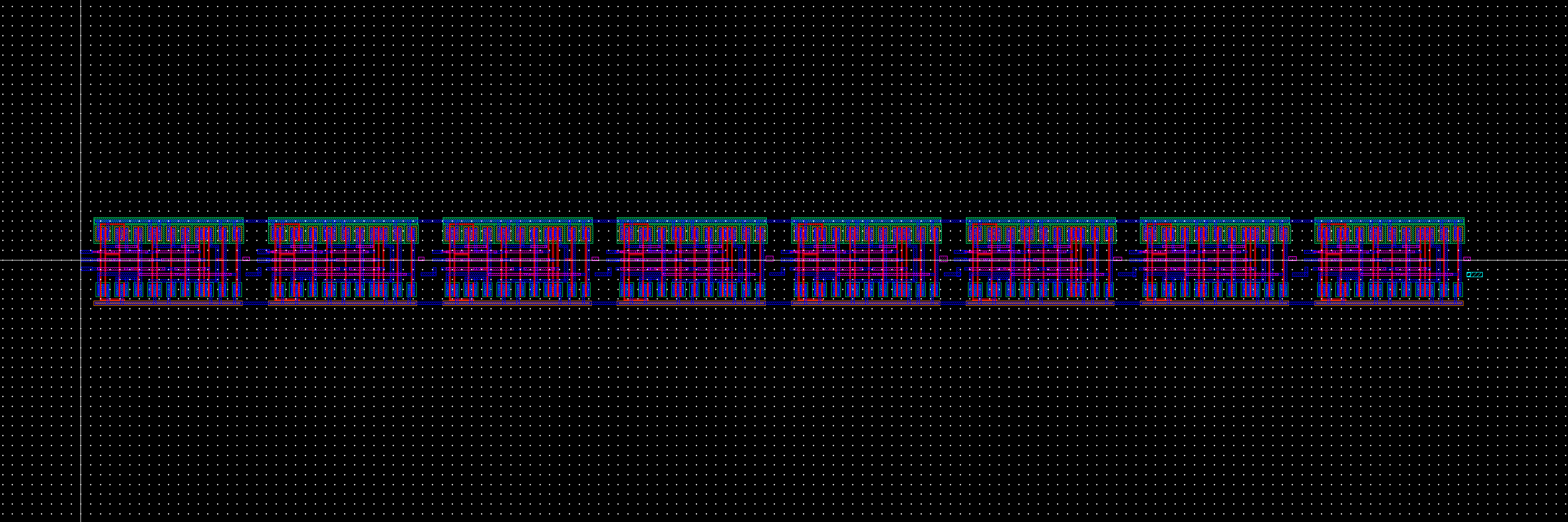
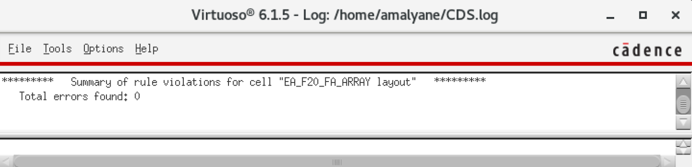
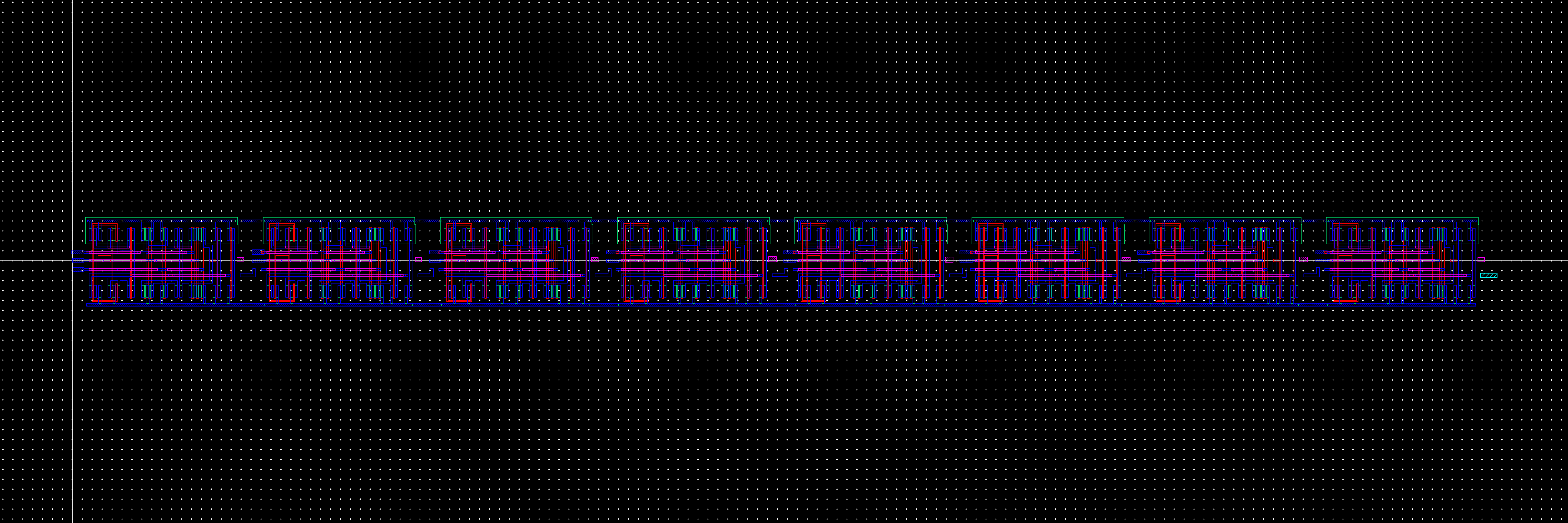
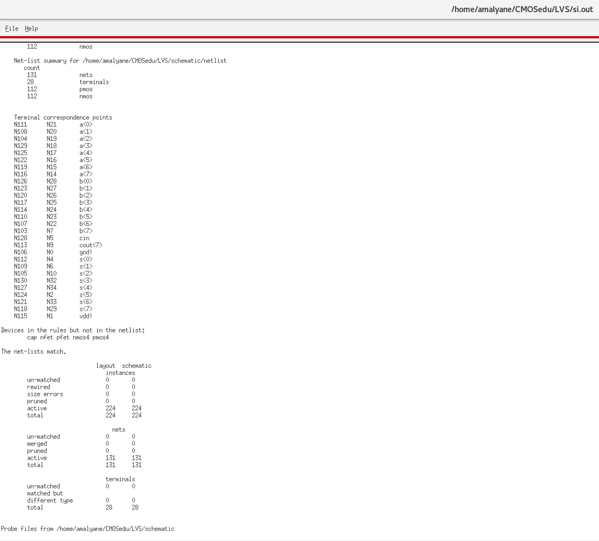
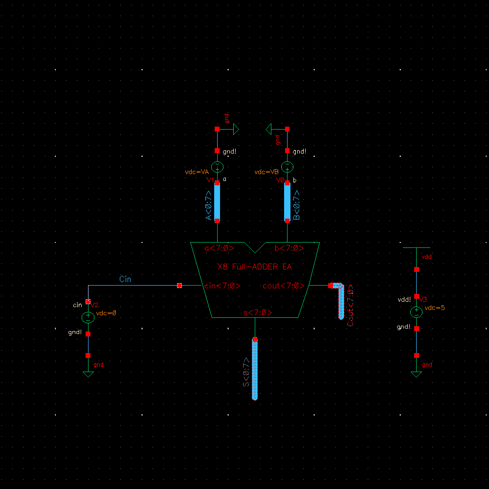
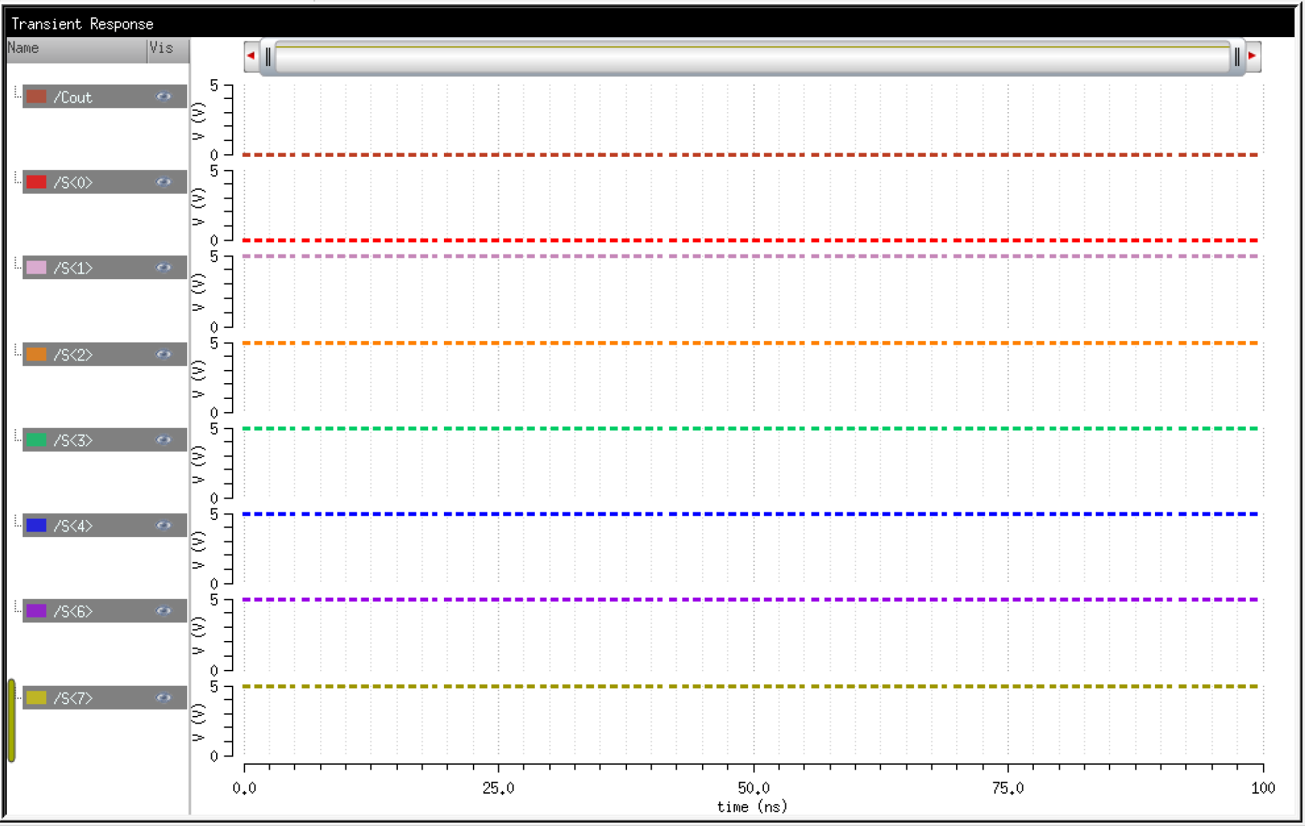
8-bit Array Full-Adder
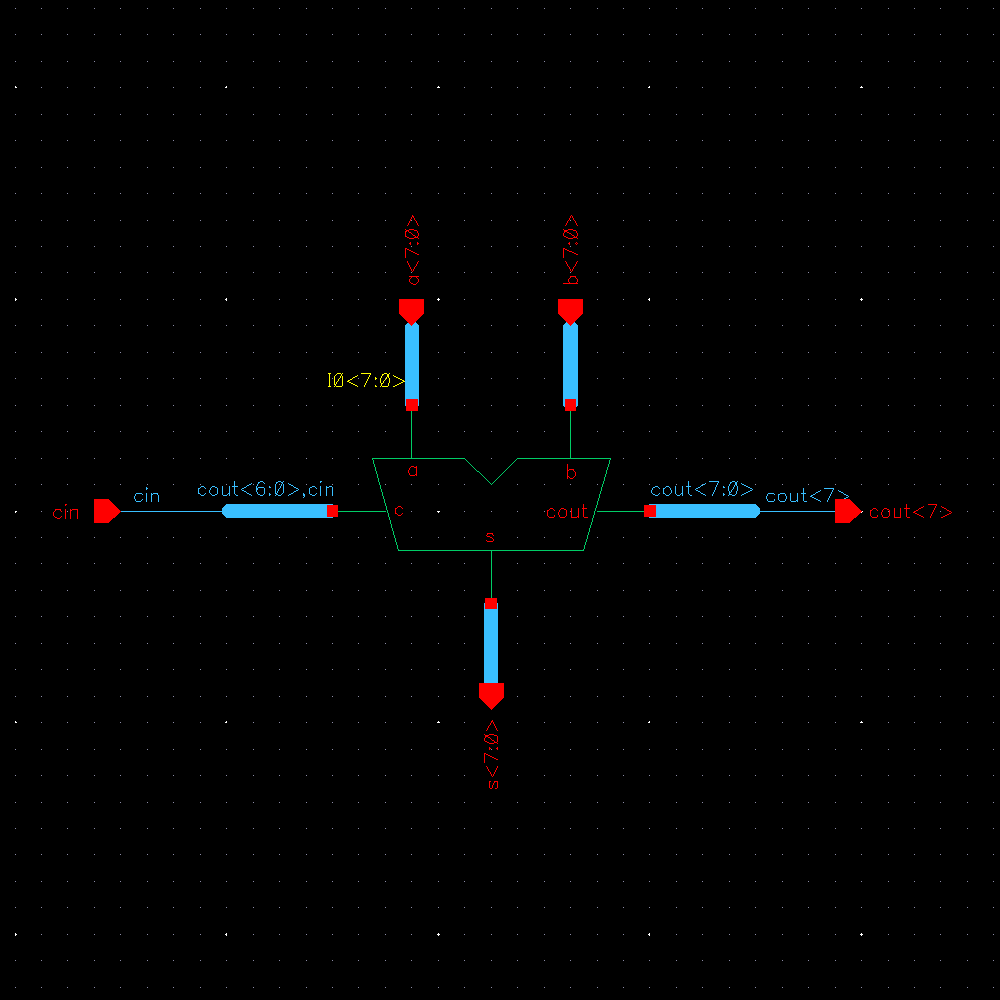
To verify the operation of my 8-bit Array FA, I added two numbers. In simulation paramters, I had A = 10111001 (185) + B = 01000101 (69) = 11111110 (254)
Backups:
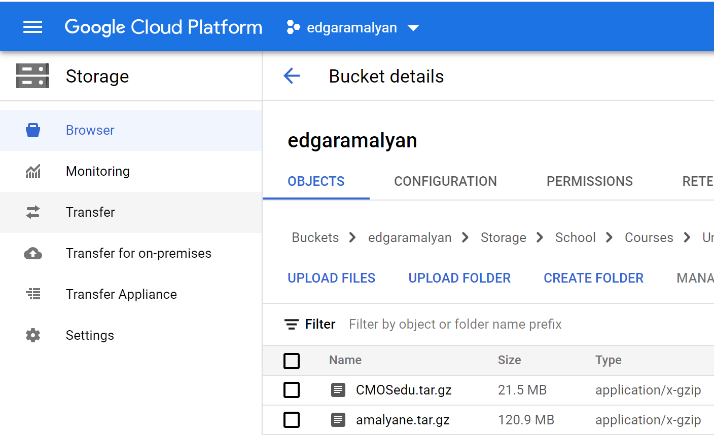
As
demonstrated in Lab 1, I run ./backup.sh from the Cadence server and
download the 'Backup' folder containing the compressed archives of my
CMOSedu and entire home directories.
All files pertaining to this lab report already exist and are directly edited from another folder that also gets synced.
I run sync_to_gcp.bat from my computer which makes my GCP Storage bucket identical to my local directory.
Return to EE 421L Labs