Lab 6 - EE 421L
Author: Edgar Amalyan
Email: amalyane@unlv.nevada.edu
Date: 10/21/2020
Goals:
This lab focuses on the layout and simulations of a NAND gate, XOR gate, and Full-Adder
Prelab
Note: Click on pictures for larger views. Tutorial 4
Schematic
Symbol
Simulation
Layout and DRC
Extraction and LVS
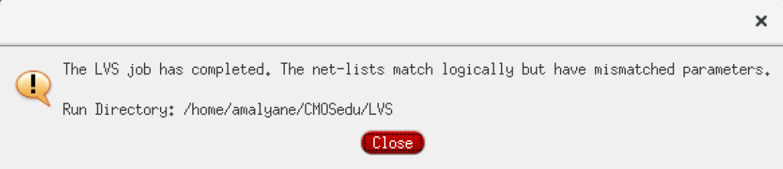
Note:
Our transistors have a width of 6um in the schematic but we have
physically drawn them to be 12um. Typically, the LVS compares only
logical netlists.
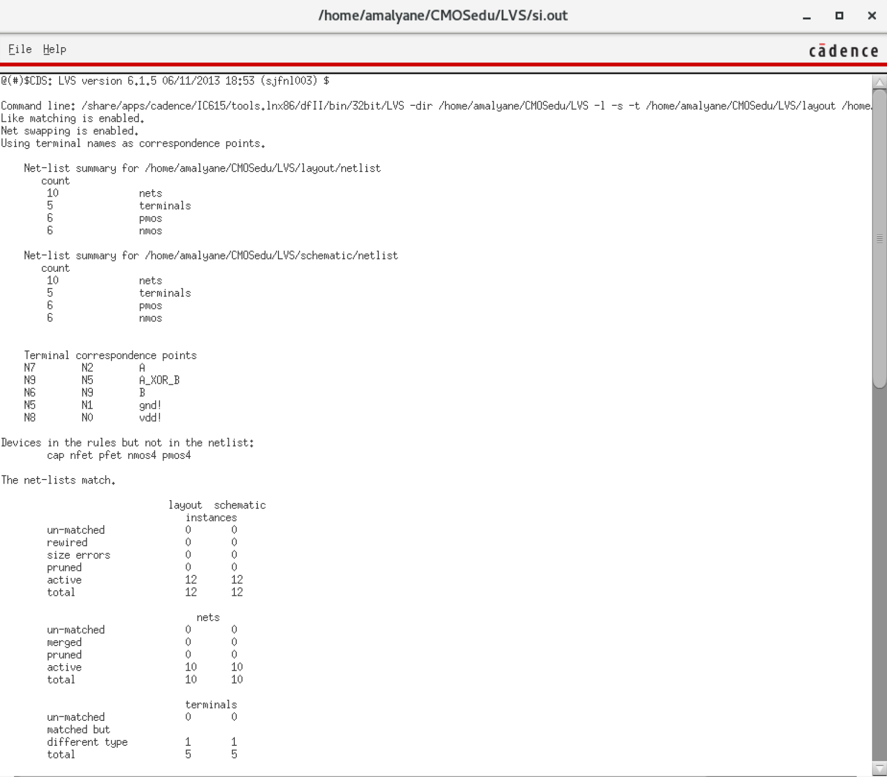
The NSCU library we use has a feature that allows the LVS to also compare the FET parameters.
Once we enable this option:
Lab
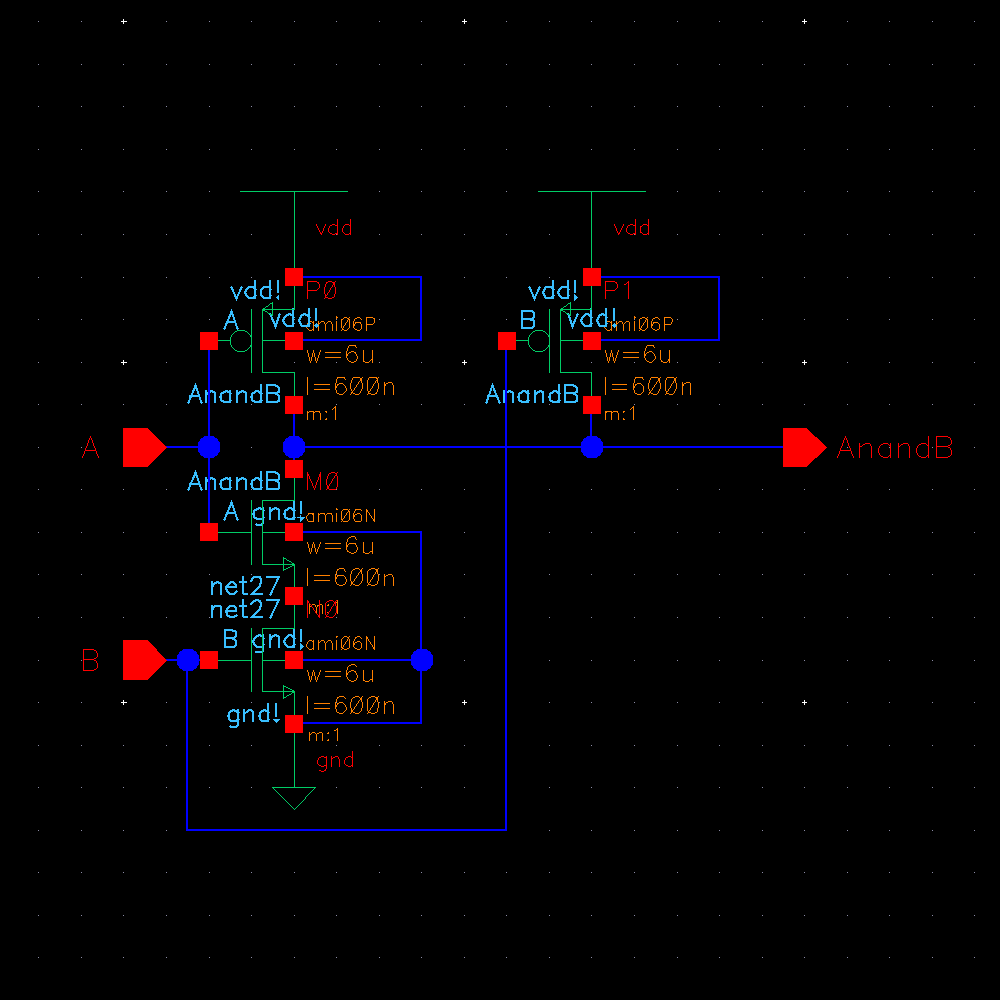
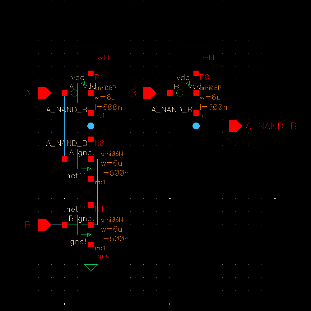
NAND Gate
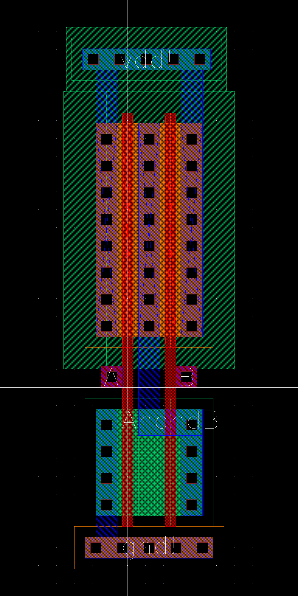
Here we will design our own NAND gate using 6u/0.6u NMOS and PMOS MOSFETs.
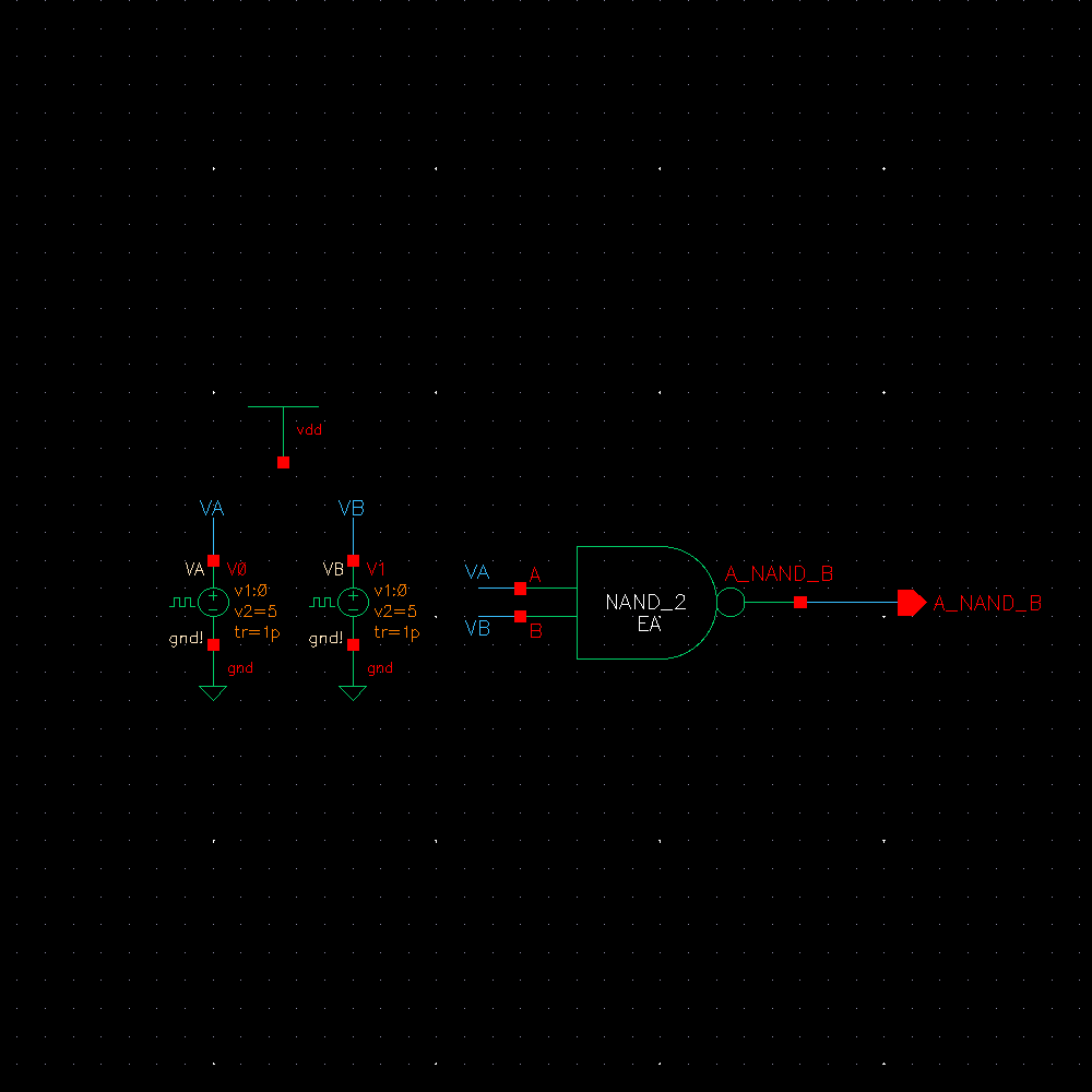
We start by drafting the schematic. A NAND gate is composed of 2 NMOS and 2 PMOS transistors.
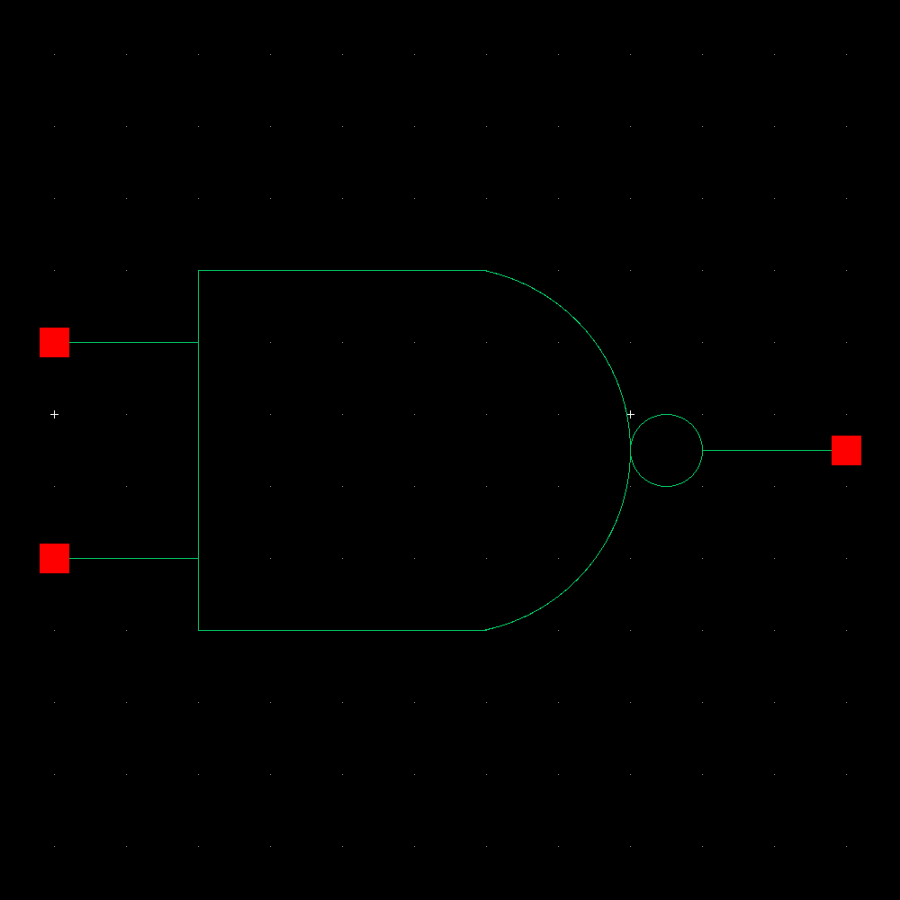
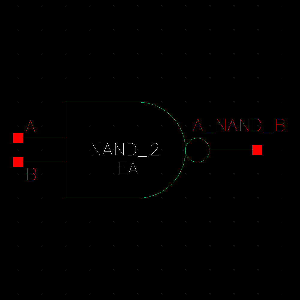
We draw the commonly used ANSI symbol for the NAND gate.
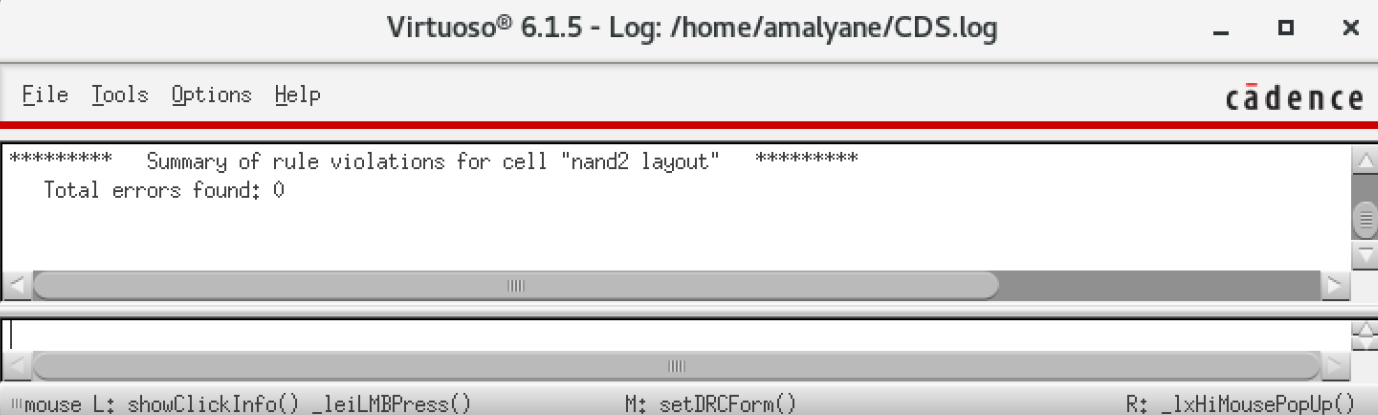
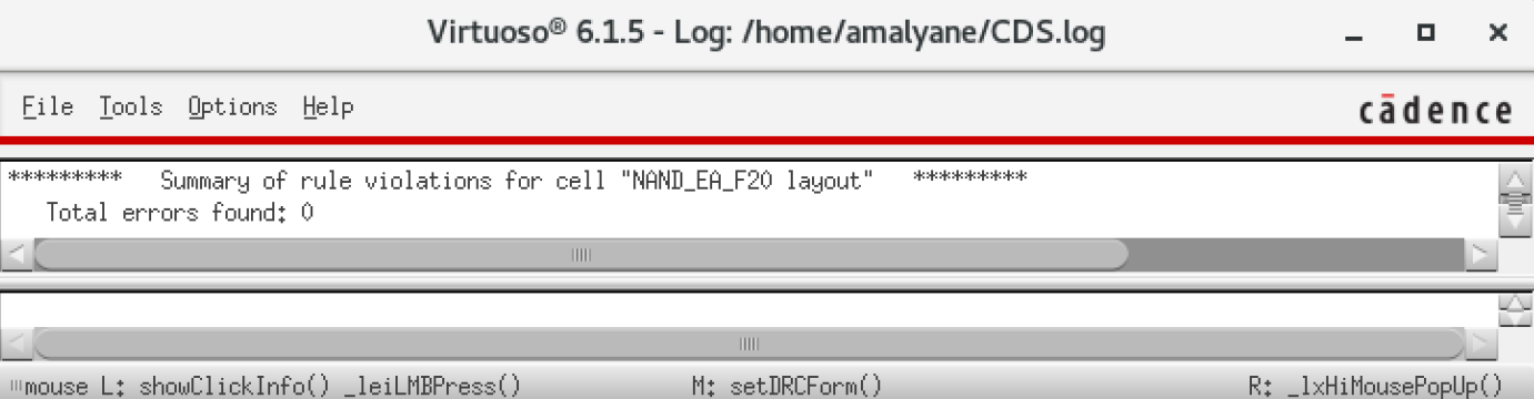
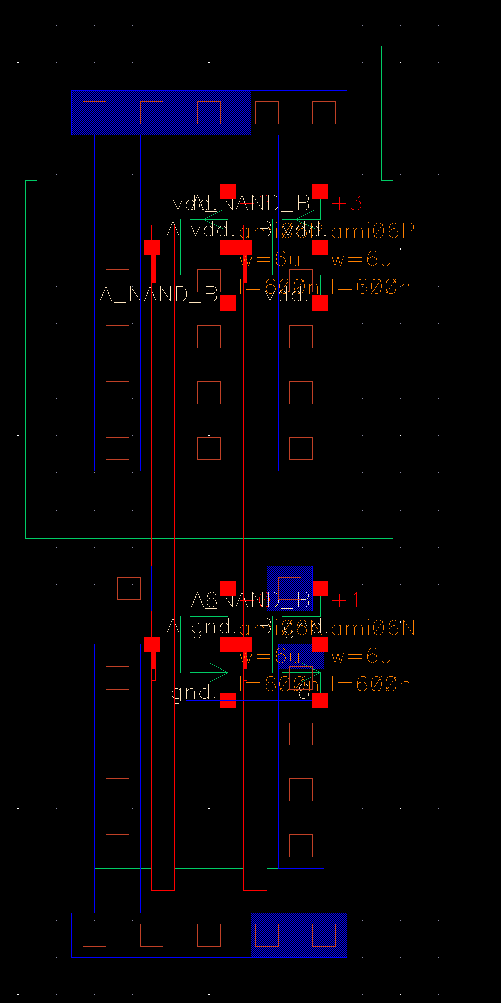
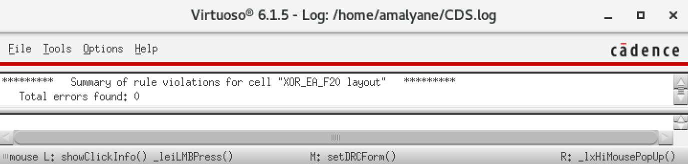
We can now proceed to the layout. We DRC after.
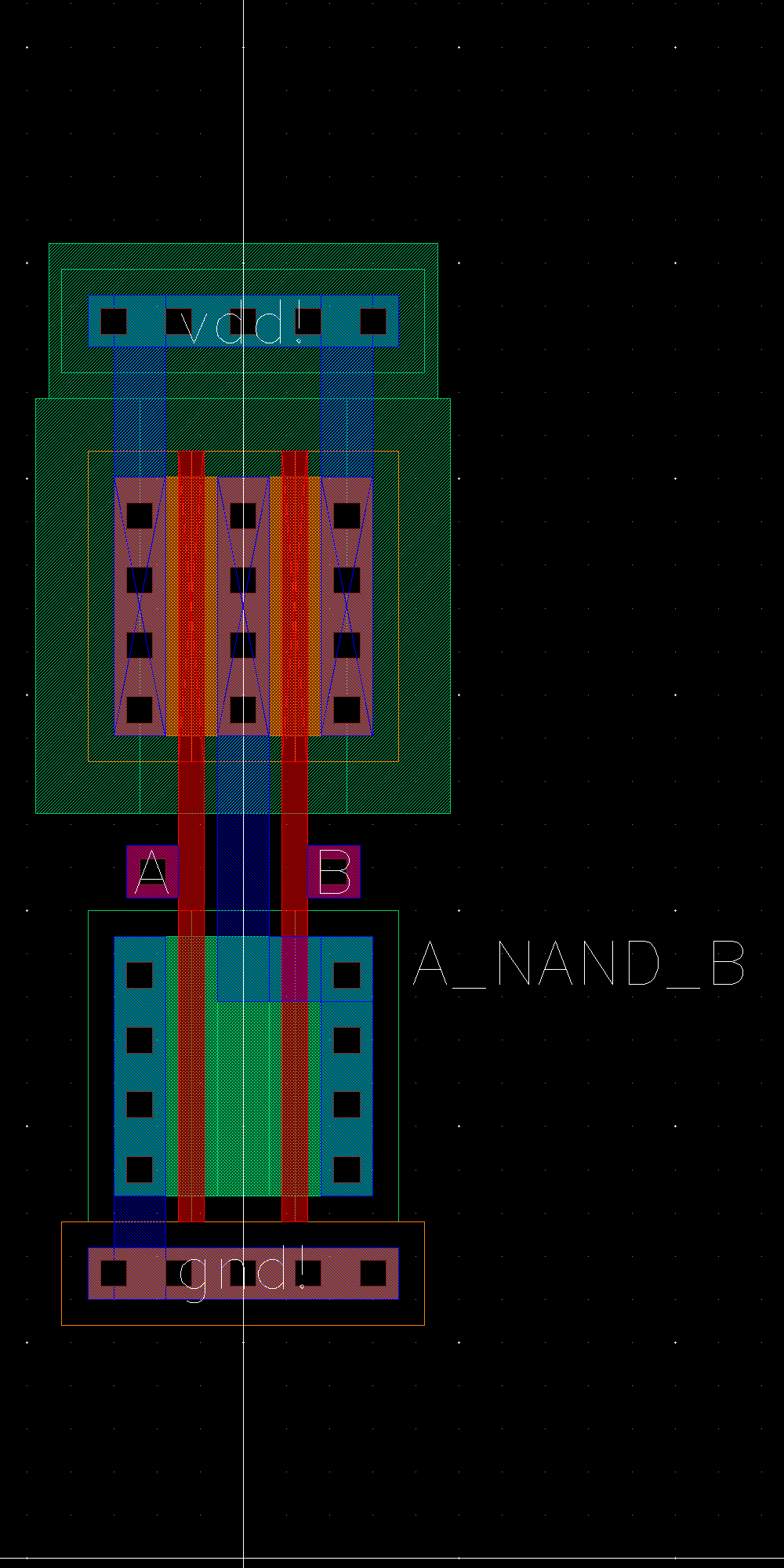
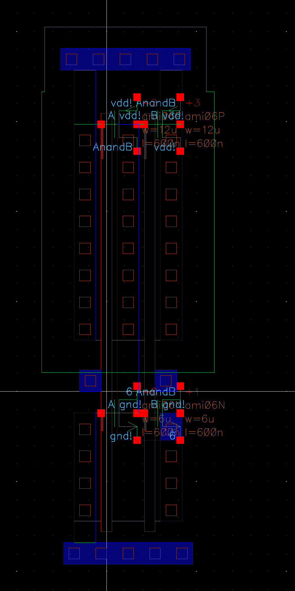
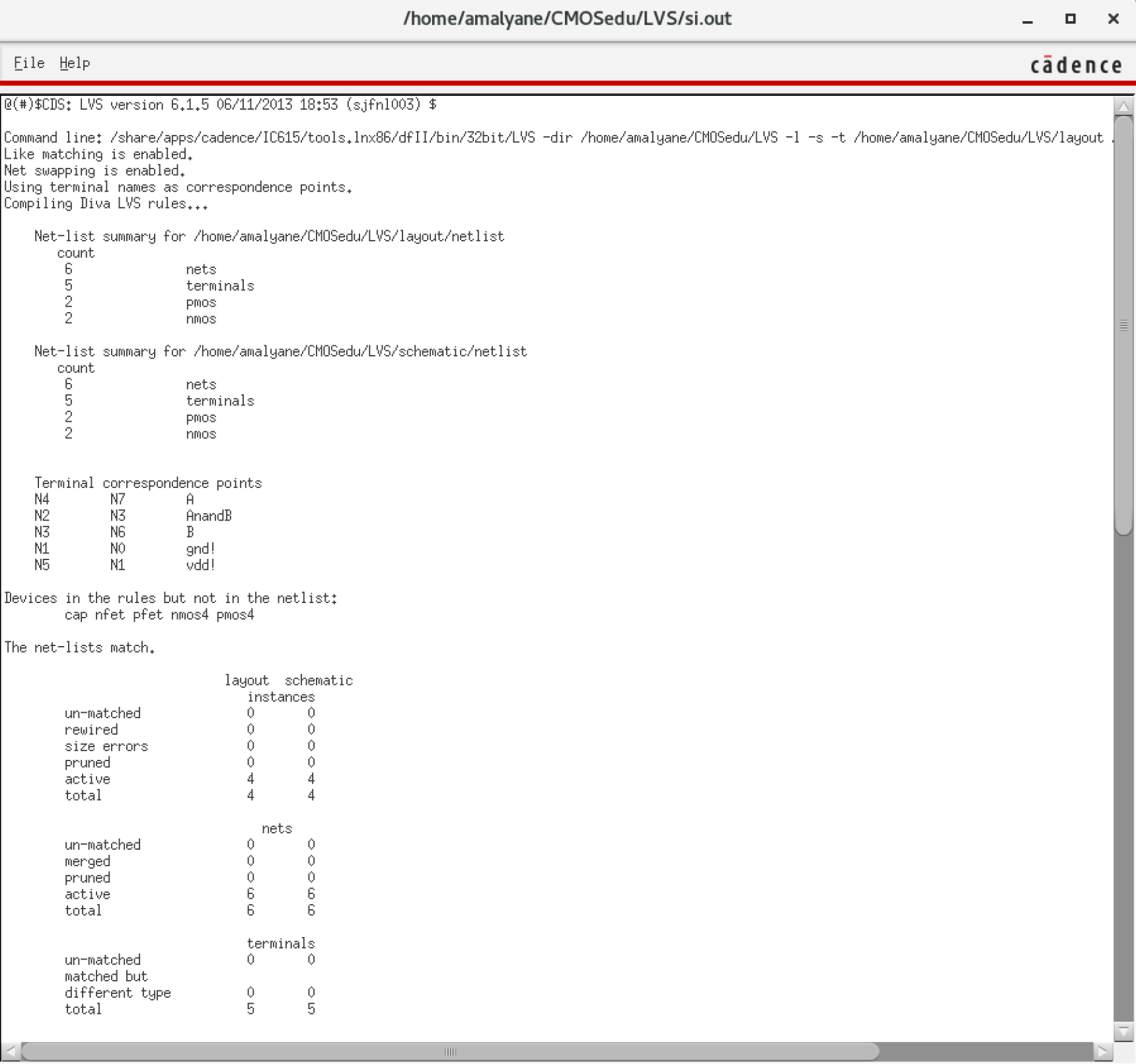
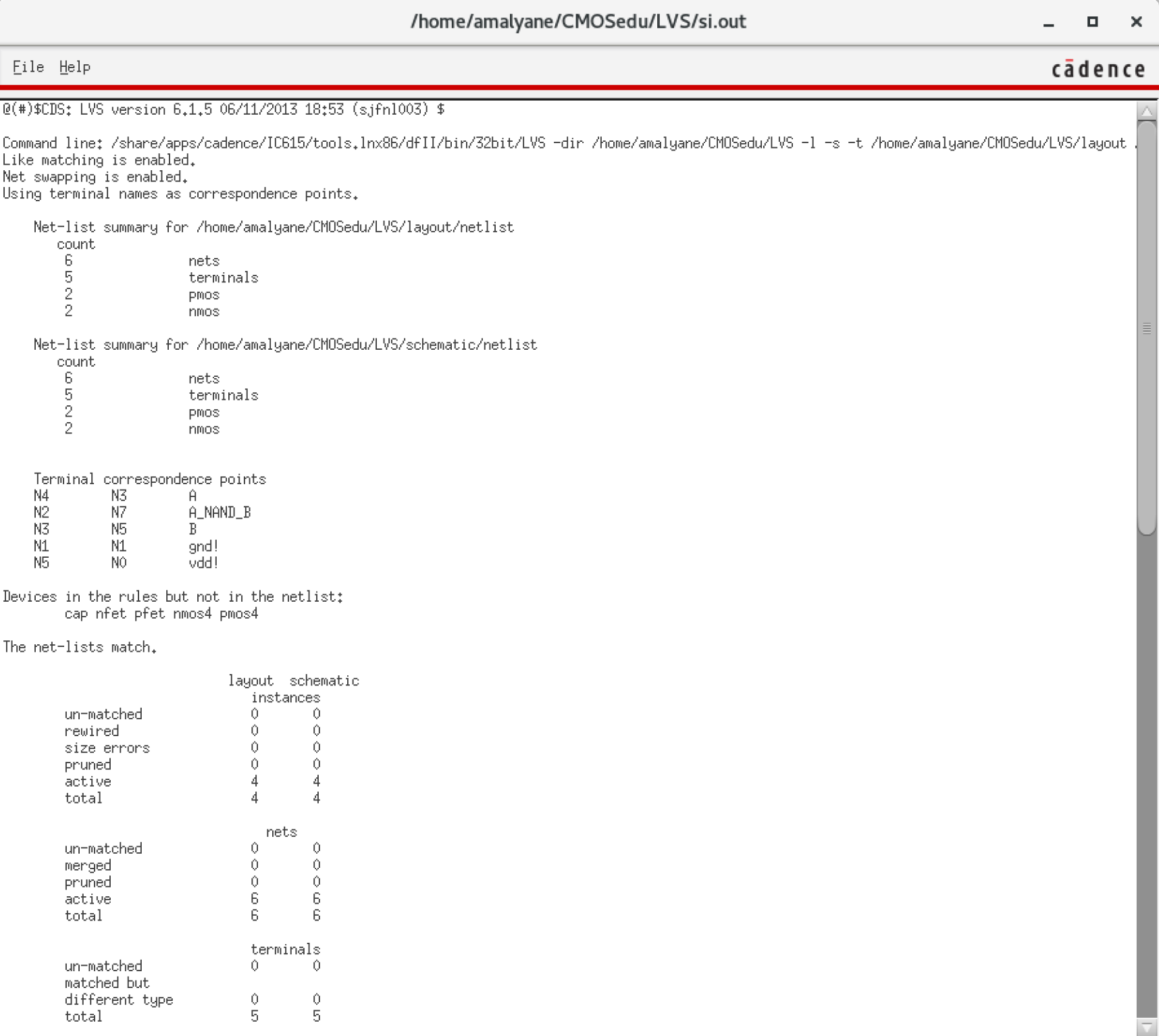
Extraction and LVS with FET comparision.
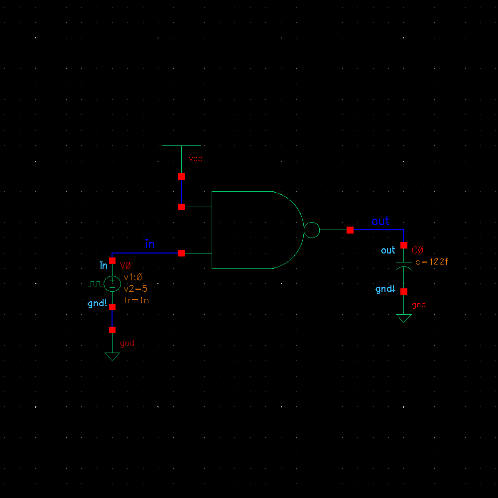
We
can now simulate our NAND gate. A NAND gate is the complement of the
AND gate. A NAND gate outputs logic 1 unless both inputs are 1.
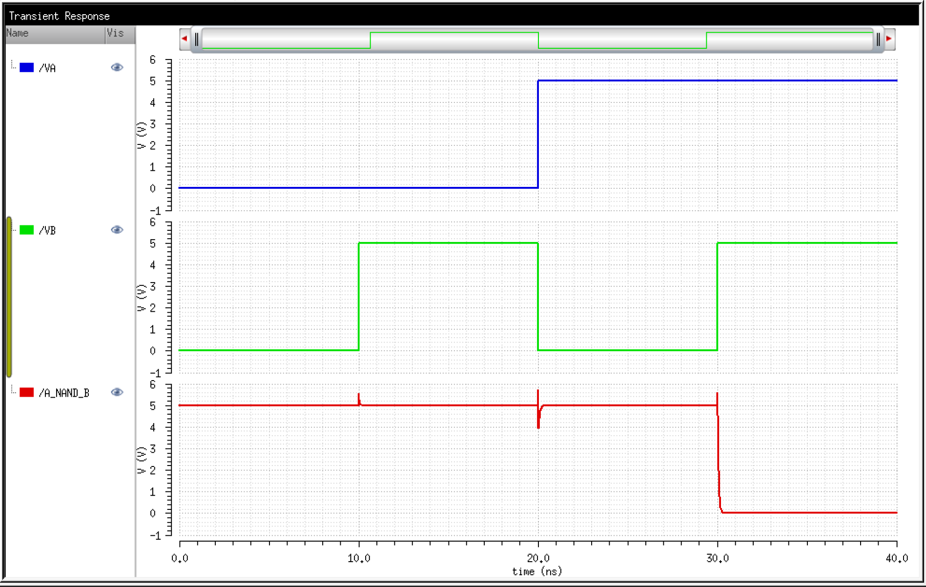
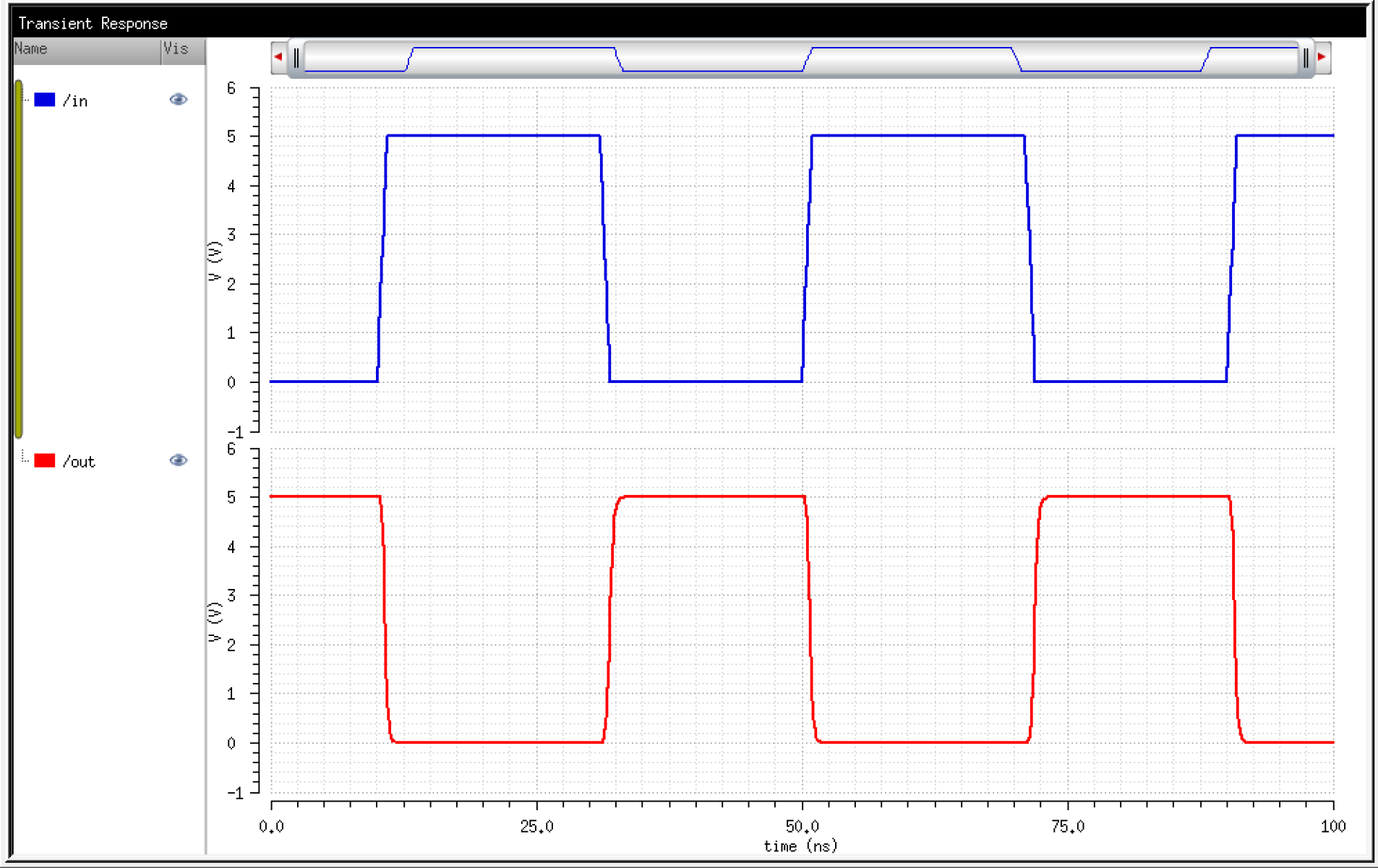
We
can notice from the above simulations some spikes in the output. These
occur during changes in the inputs. The transistor is in an undefined
state as it is neither 0 nor 1.
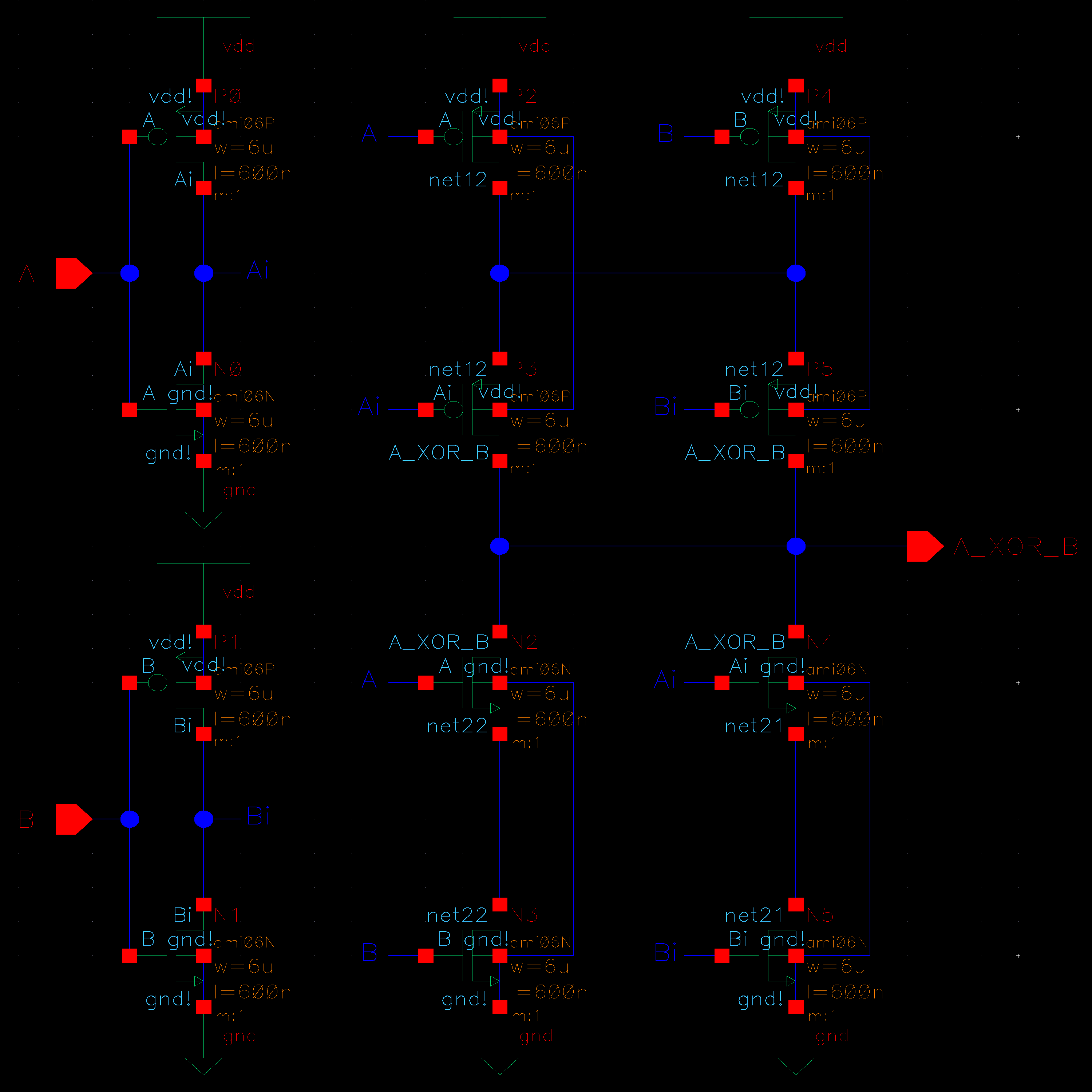
XOR Gate
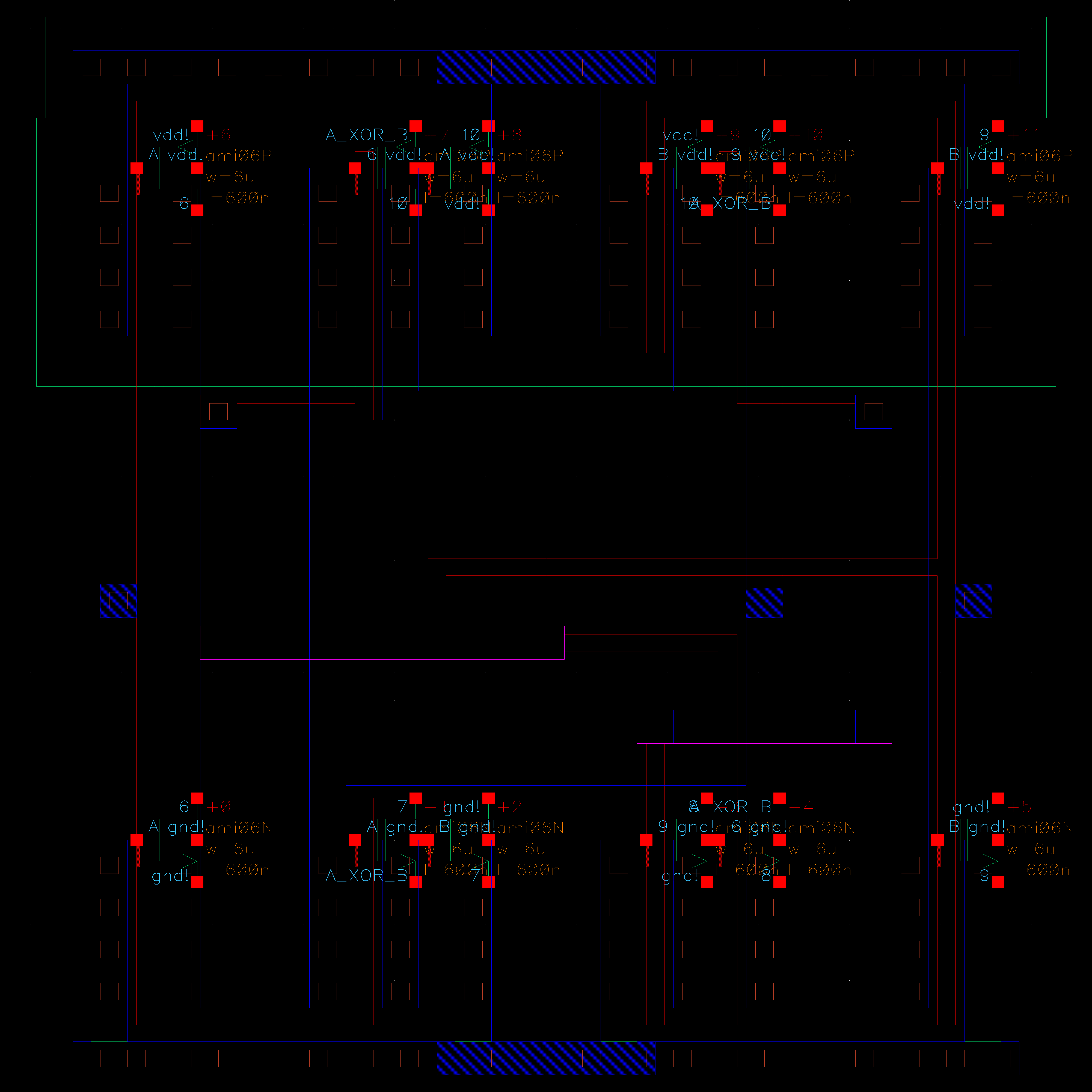
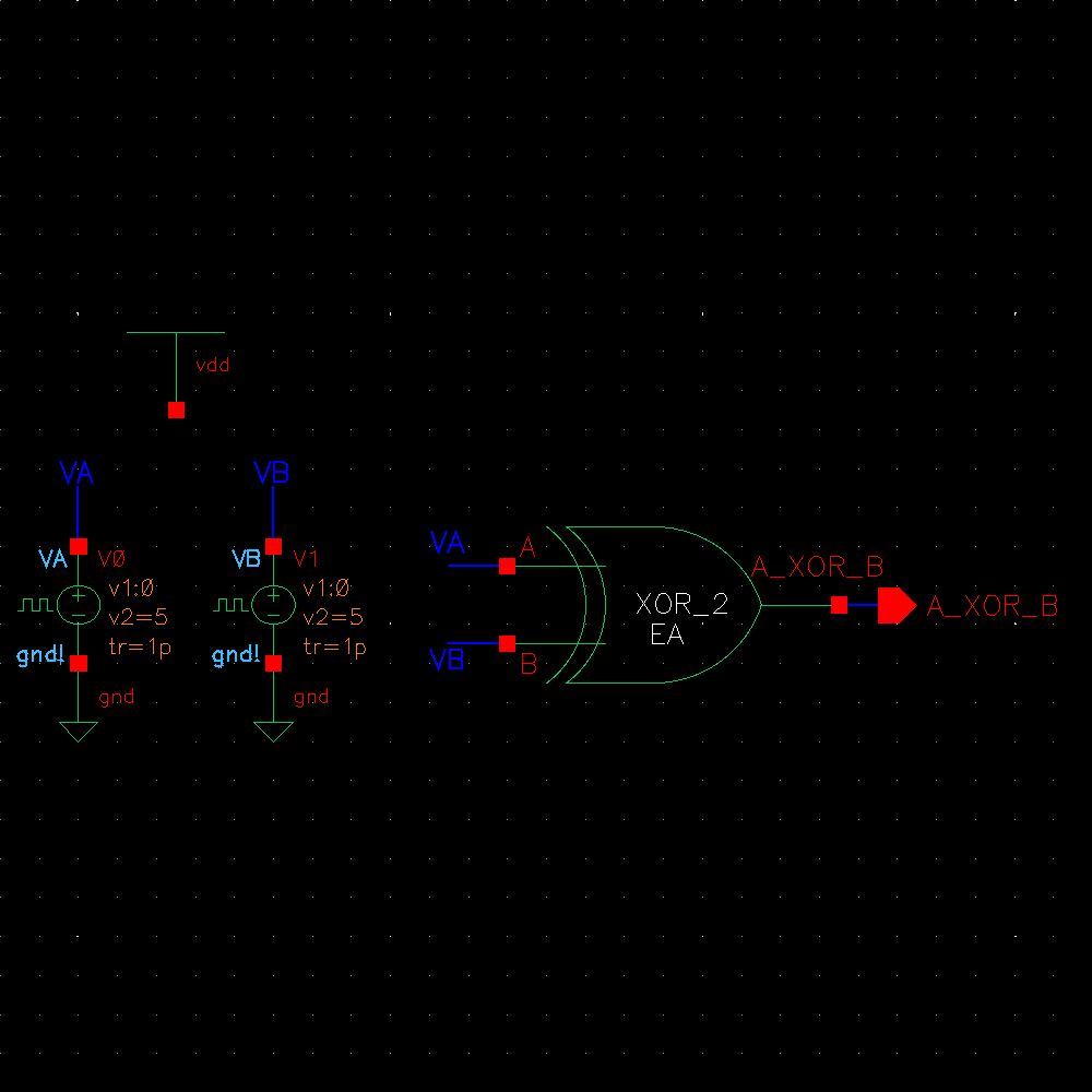
Here we will design our own XOR gate using 6u/0.6u NMOS and PMOS MOSFETs.
We start by drafting the schematic. A XOR gate is composed of 6 NMOS and 6 PMOS transistors.
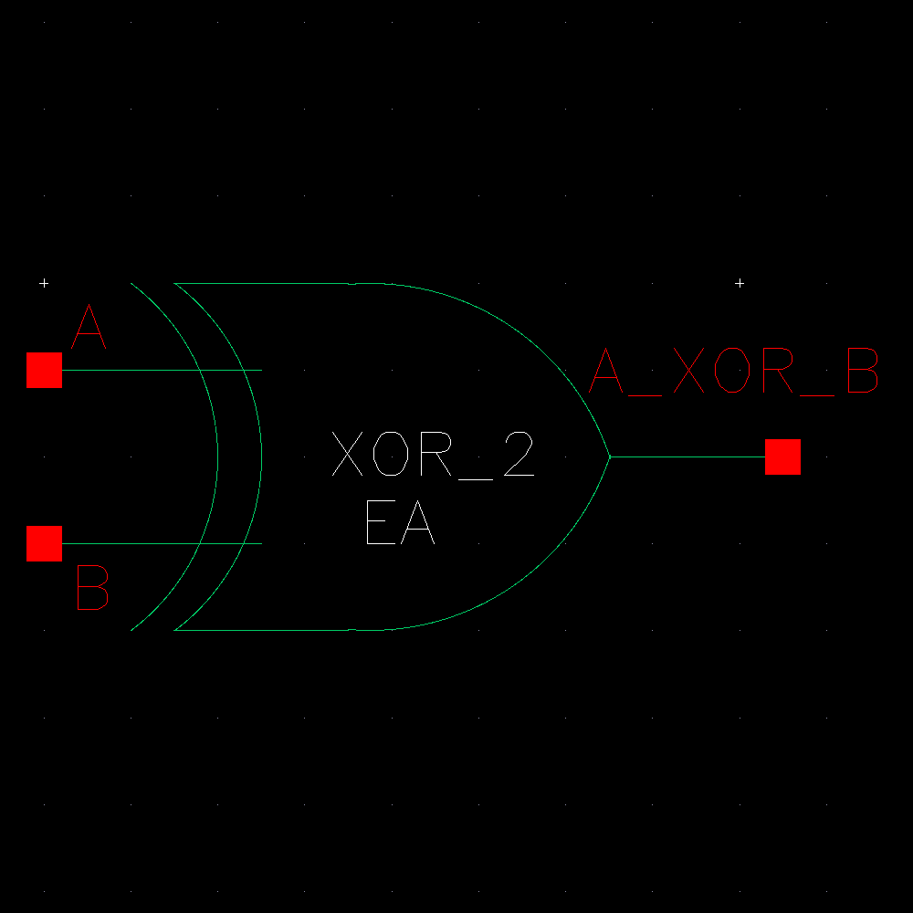
We draw the commonly used ANSI symbol for the XOR gate.
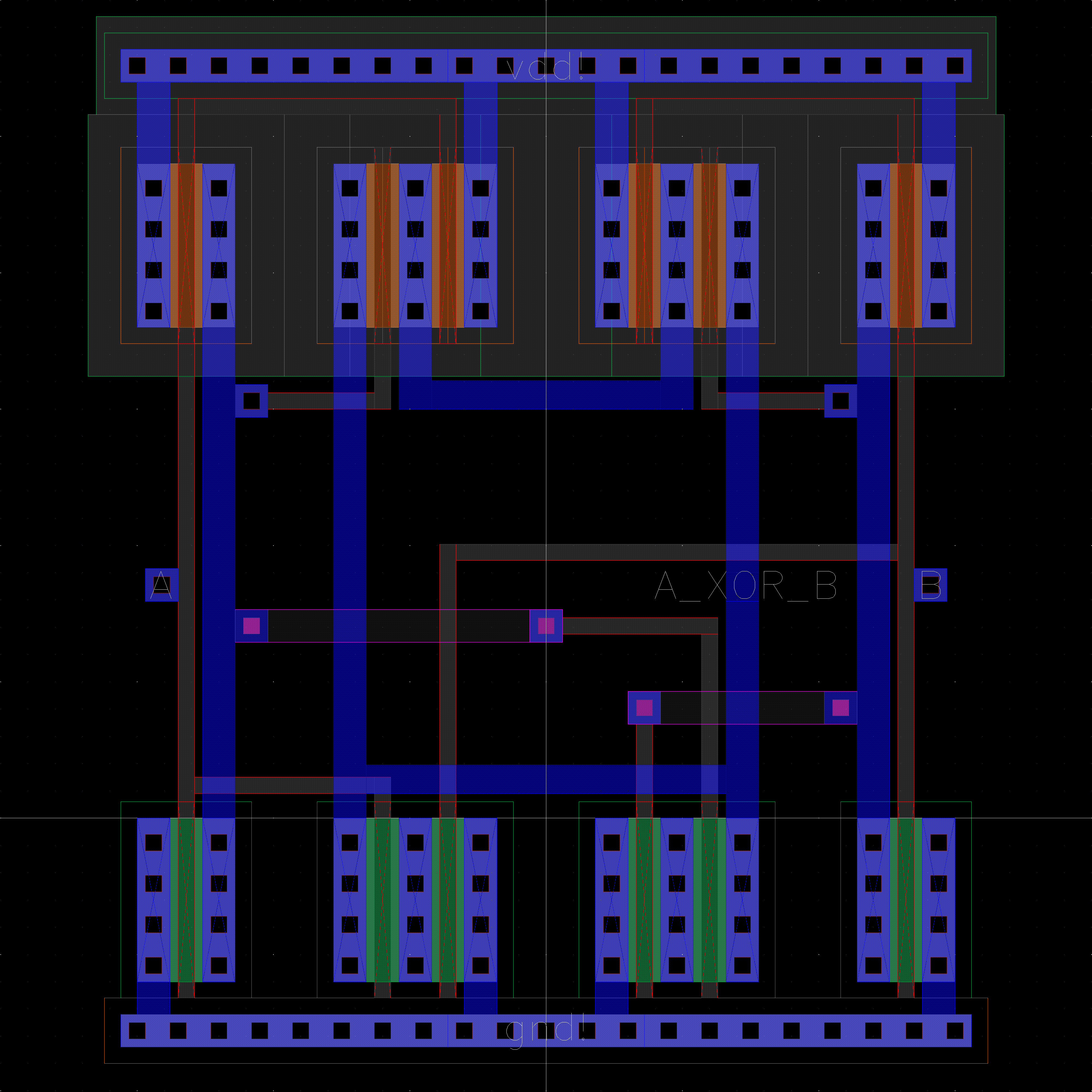
We can now proceed to the layout. We DRC after.
Extraction and LVS with FET comparision.
We
can now simulate our XOR gate. A XOR gate outputs logic 1 if either, but not both, inputs, are 1.
We
can notice from the above simulations some spikes in the output. These
occur during changes in the inputs. The transistor is in an undefined
state as it is neither 0 nor 1.
Full Adder
Here we will design our own Full Adder using 6u/0.6u NMOS and PMOS MOSFETs.
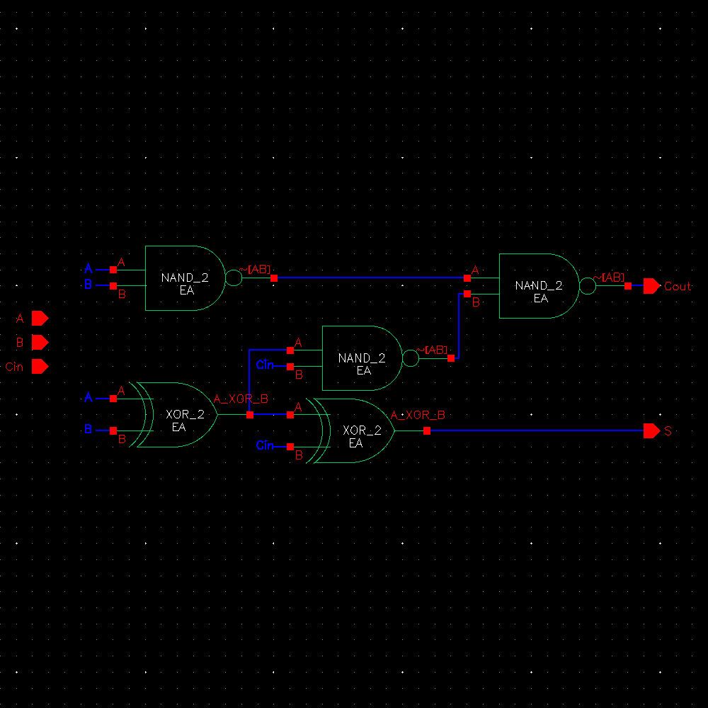
We
start by drafting the schematic. Our Full Adder is composed of 3 NAND
gates and 2 XOR gates. Therefore, it requires a total of 18 NMOS and 18
PMOS transistors.
Instead of instantiating and connecting 36 individual transistors, we can use the NAND and XOR symbols we just made.
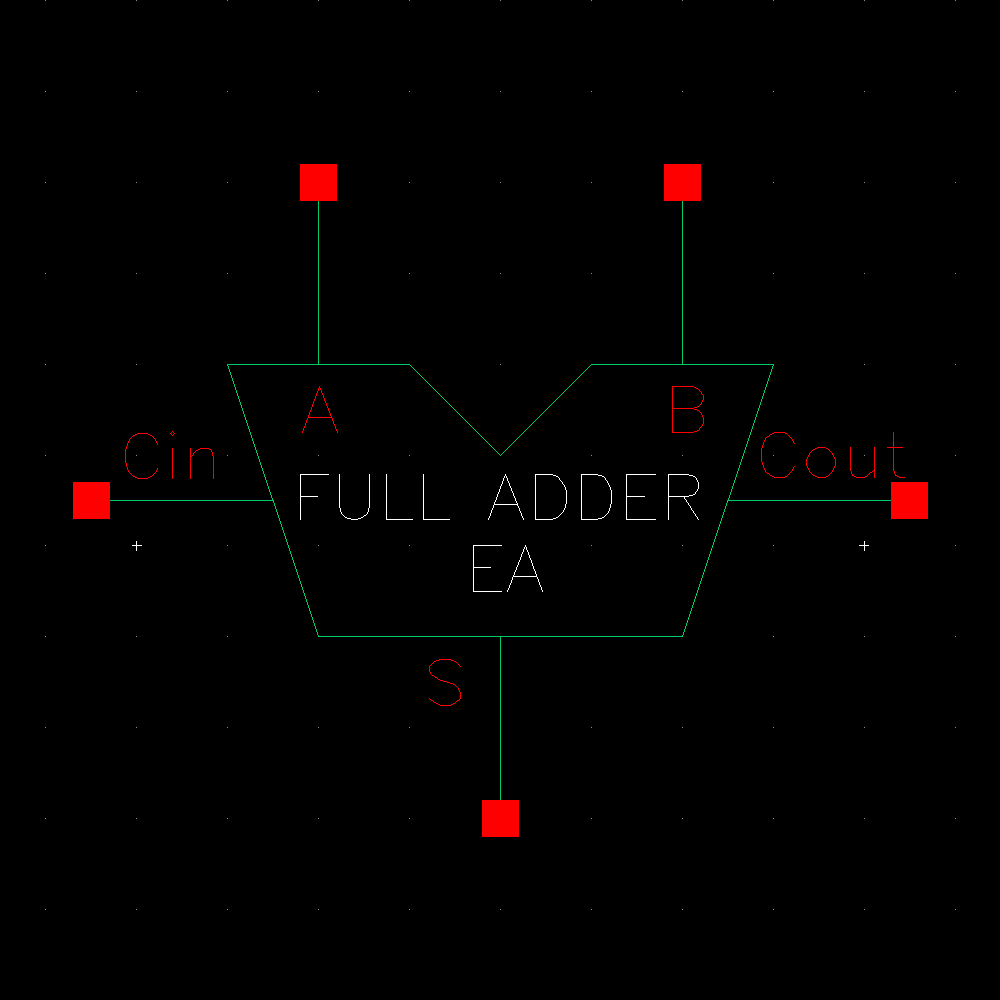
We draw the commonly used symbol for the Full Adder.
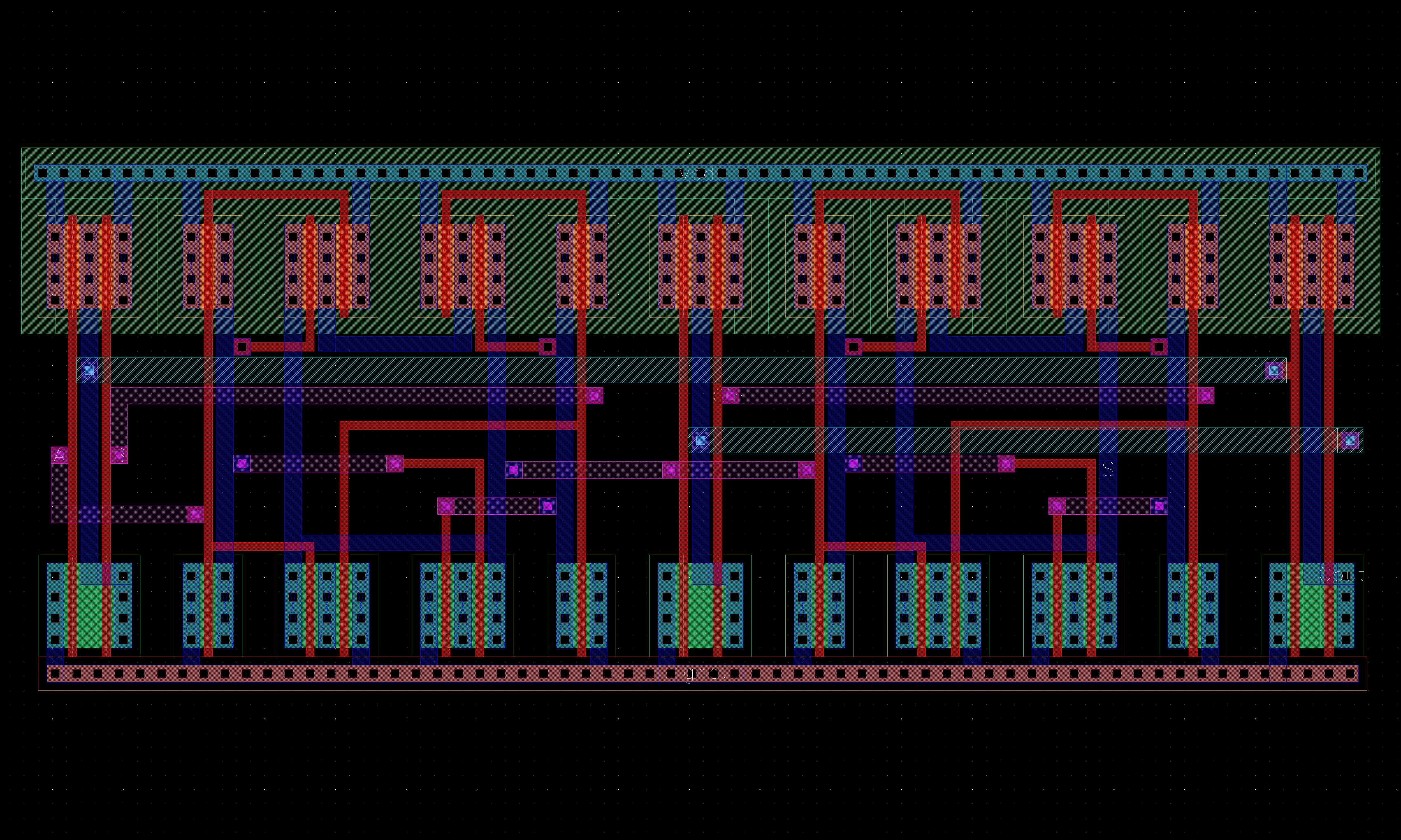
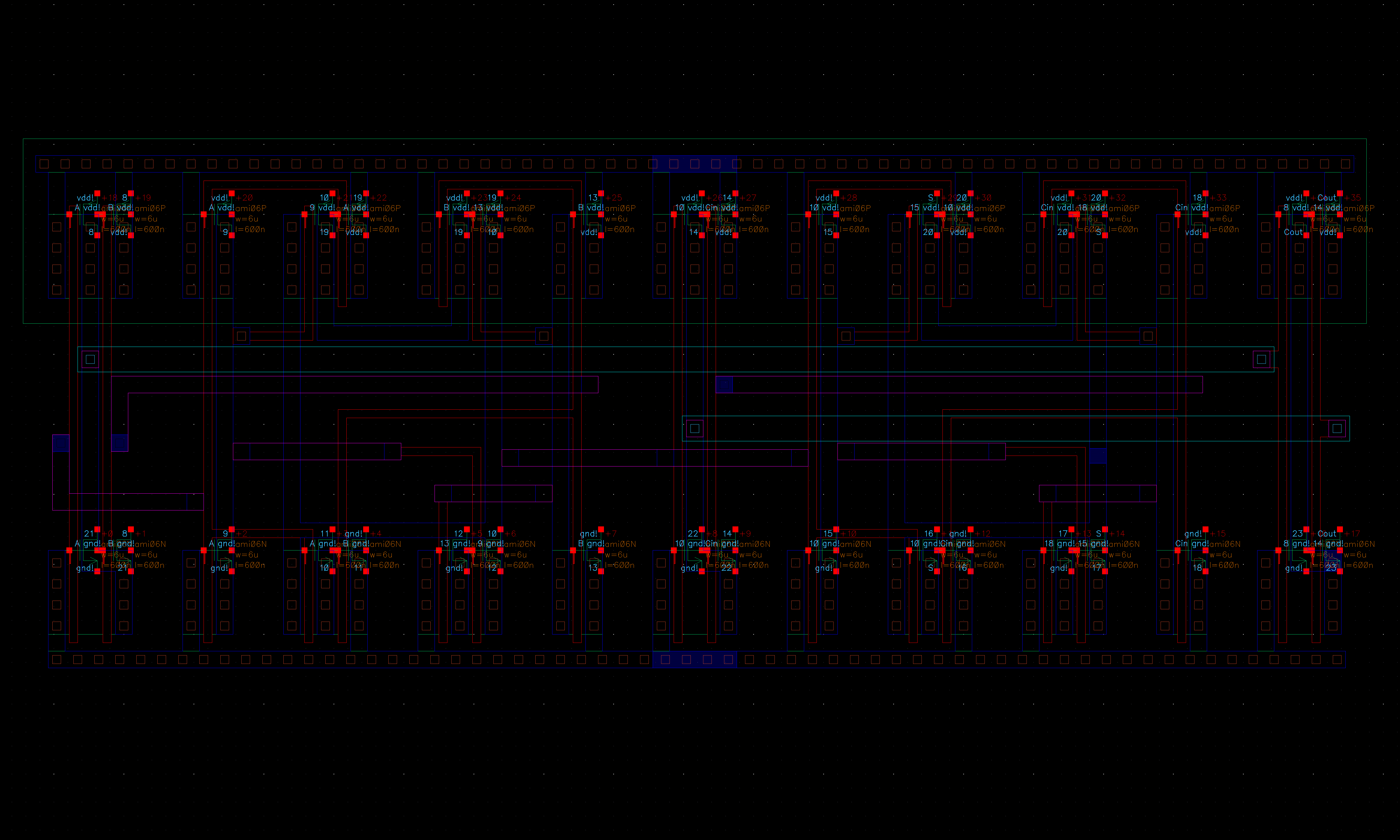
We
can now proceed to the layout. Terminal pins can be placed on metal 1
or metal 2. I choose metal 1 with a via if needed. Metal 3 can be used
for long interconnections. We DRC after.
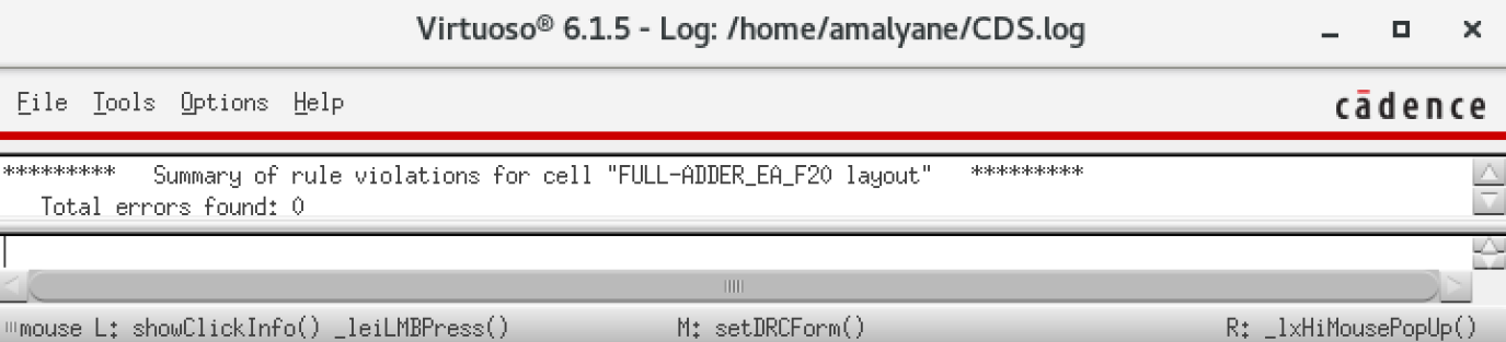
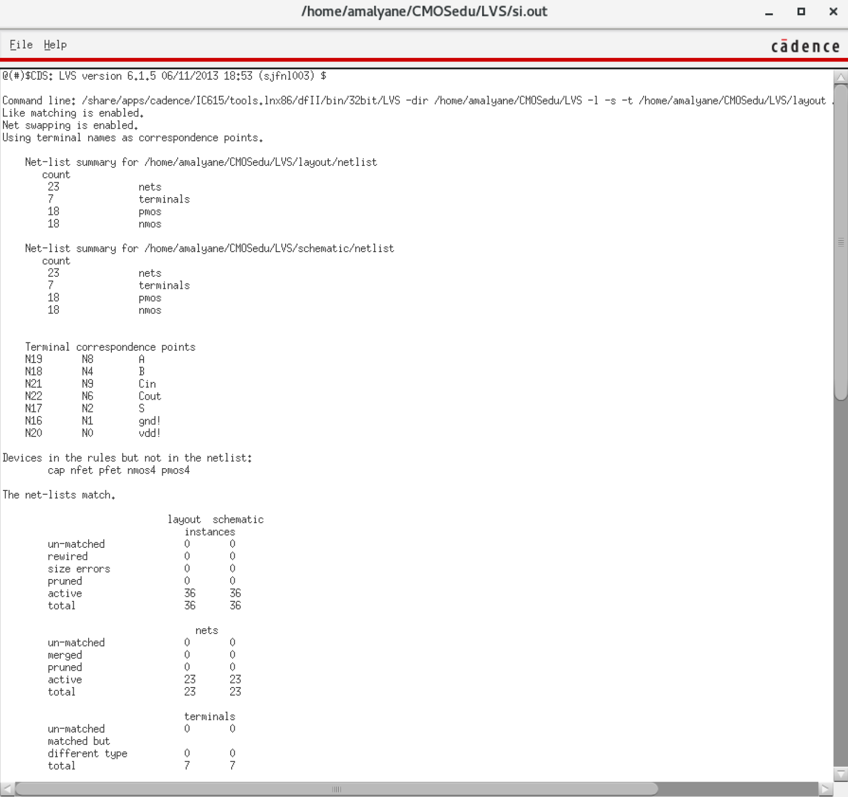
Extraction and LVS with FET comparision.
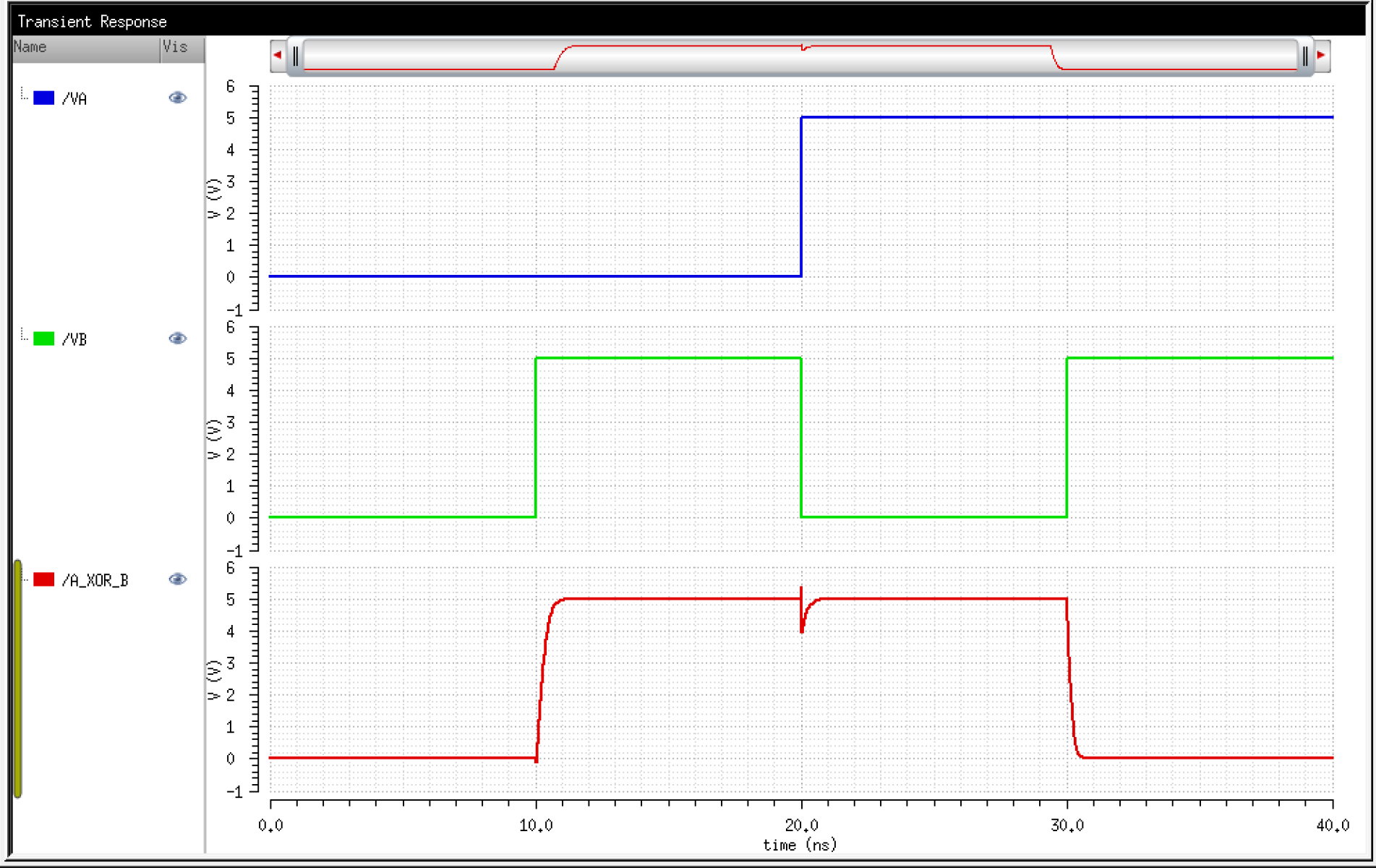
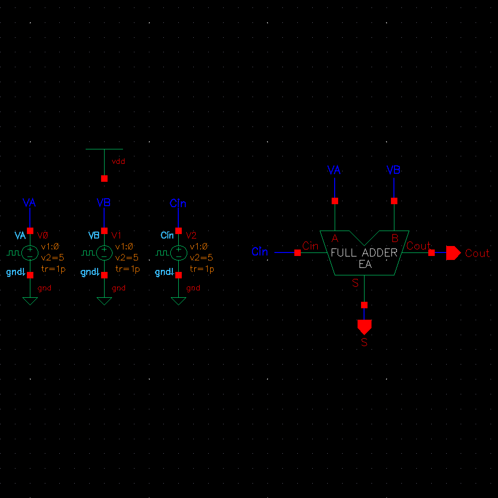
We
can now simulate our Full Adder. A full adder simply adds 2 inputs.
Since the output, S, is only 1 bit, the result will overflow and be 0
when the inputs, A and B, are 1. Therefore, a carry out, Cout, should
be generated. We add this as another output. As we can see, there are
now 3 inputs that can be added, so we add another input, Cin, which
could be any value, or just the Cout from the last addition. Now if all
3 inputs are 1, then both S and Cout are 1 and we have enough bits to
represent any combination. This idea can be expanded into an n-bit Full
Adder.
As seen below, the simulations match the generic truth table of a Full Adder.
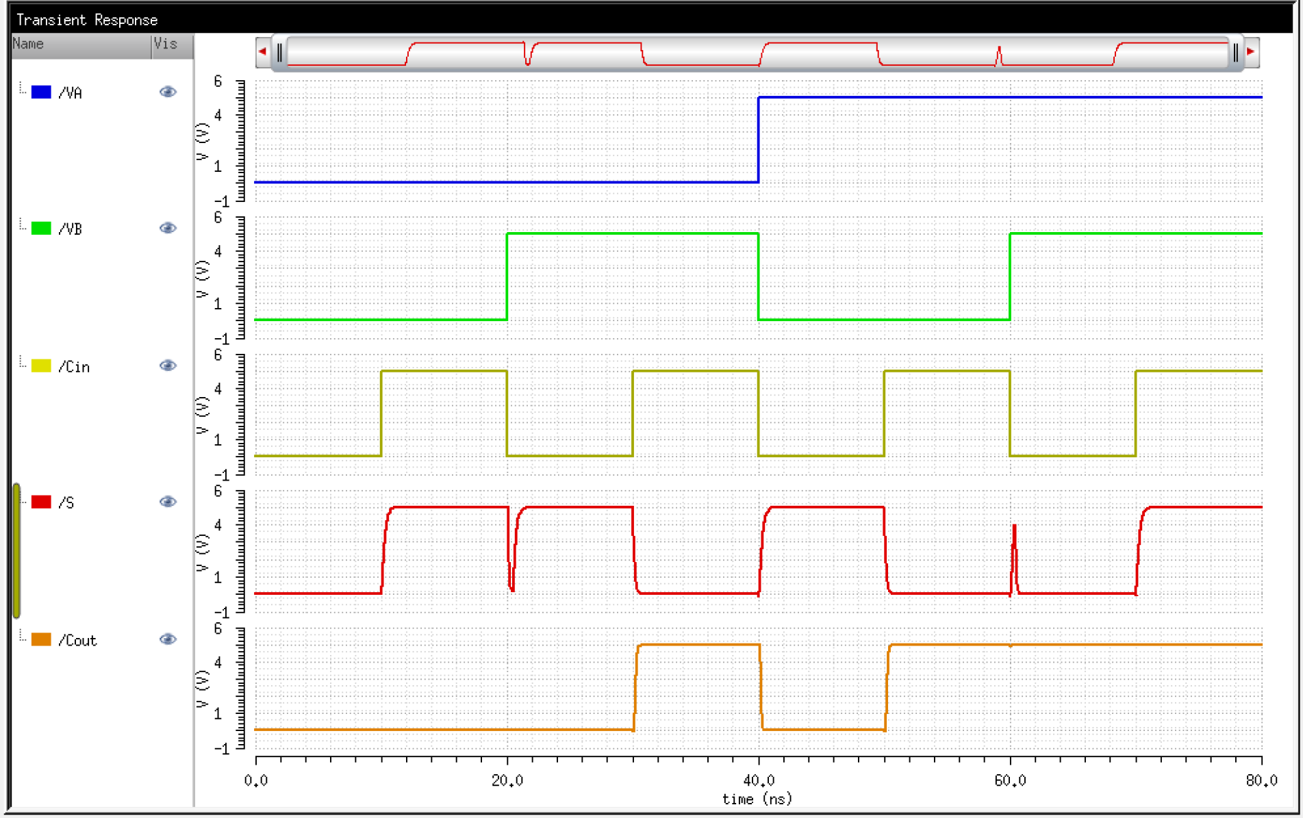
We
can notice from the above simulations some spikes in the output. These
occur during changes in the inputs. The transistor is in an undefined
state as it is neither 0 nor 1. We can go ahead and ignore the glitches
and just assume the value before and after the glitch remains constant.
Backups:
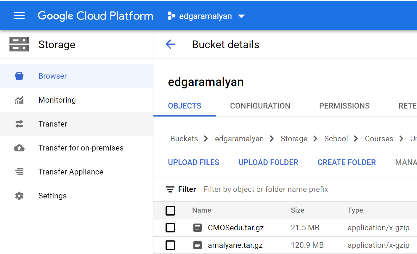
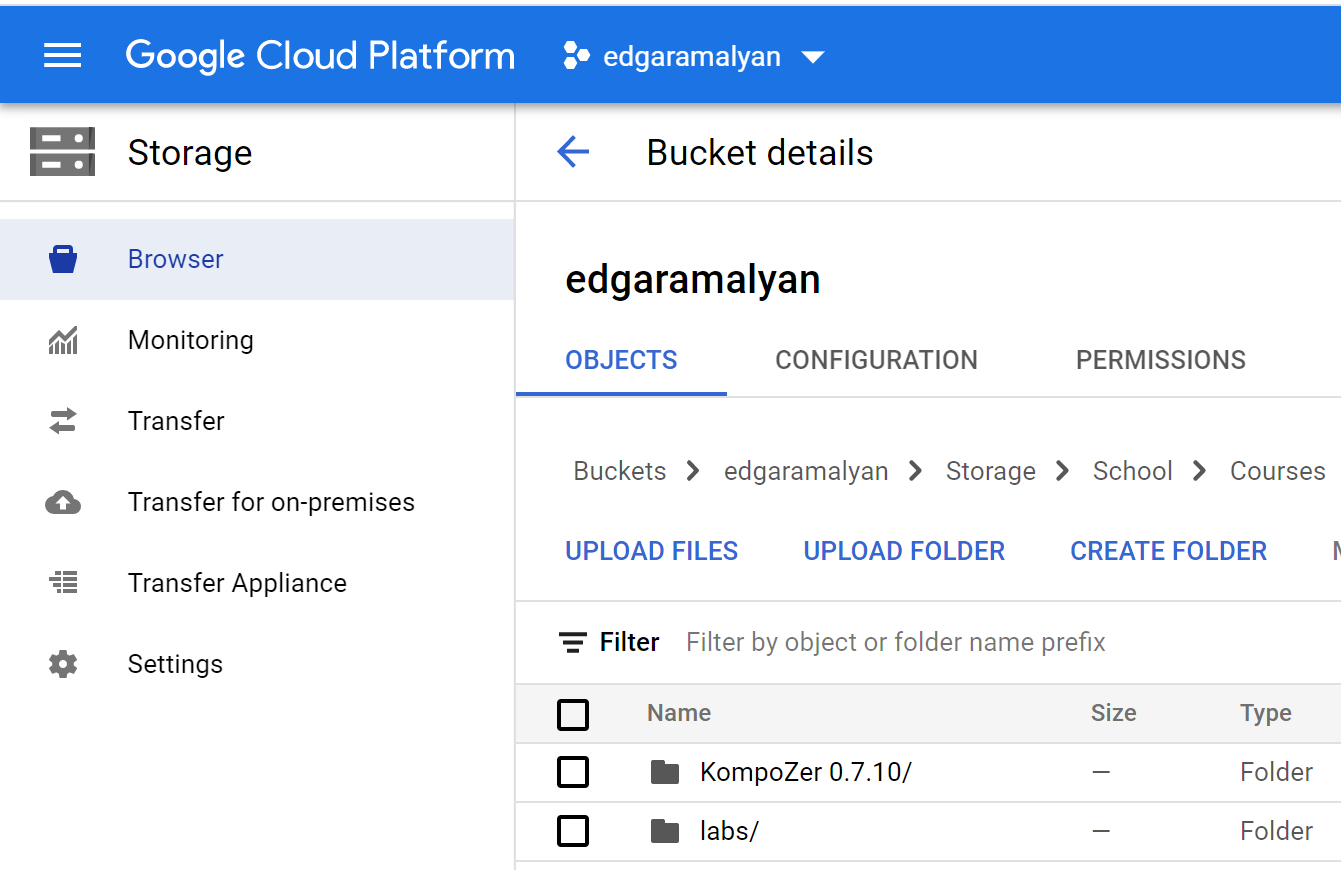
As
demonstrated in Lab 1, I run ./backup.sh from the Cadence server and
download the 'Backup' folder containing the compressed archives of my
CMOSedu and entire home directories.
All files pertaining to this lab report already exist and are directly edited from another folder that also gets synced.
I run sync_to_gcp.bat from my computer which makes my GCP Storage bucket identical to my local directory.
Return to EE 421L Labs