Lab 4 - EE 421L
Author: Edgar Amalyan
Email: amalyane@unlv.nevada.edu
Date: 09/23/2020
Goals:
This lab focuses on the layout and simulations (IV curves) of NMOS and PMOS transistors.
Prelab
Note: Click on pictures for larger views.
Tutorial 2
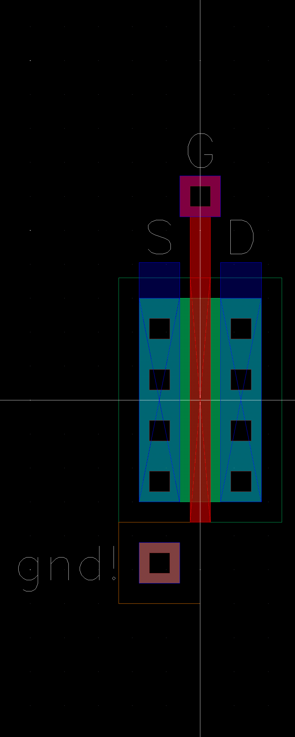
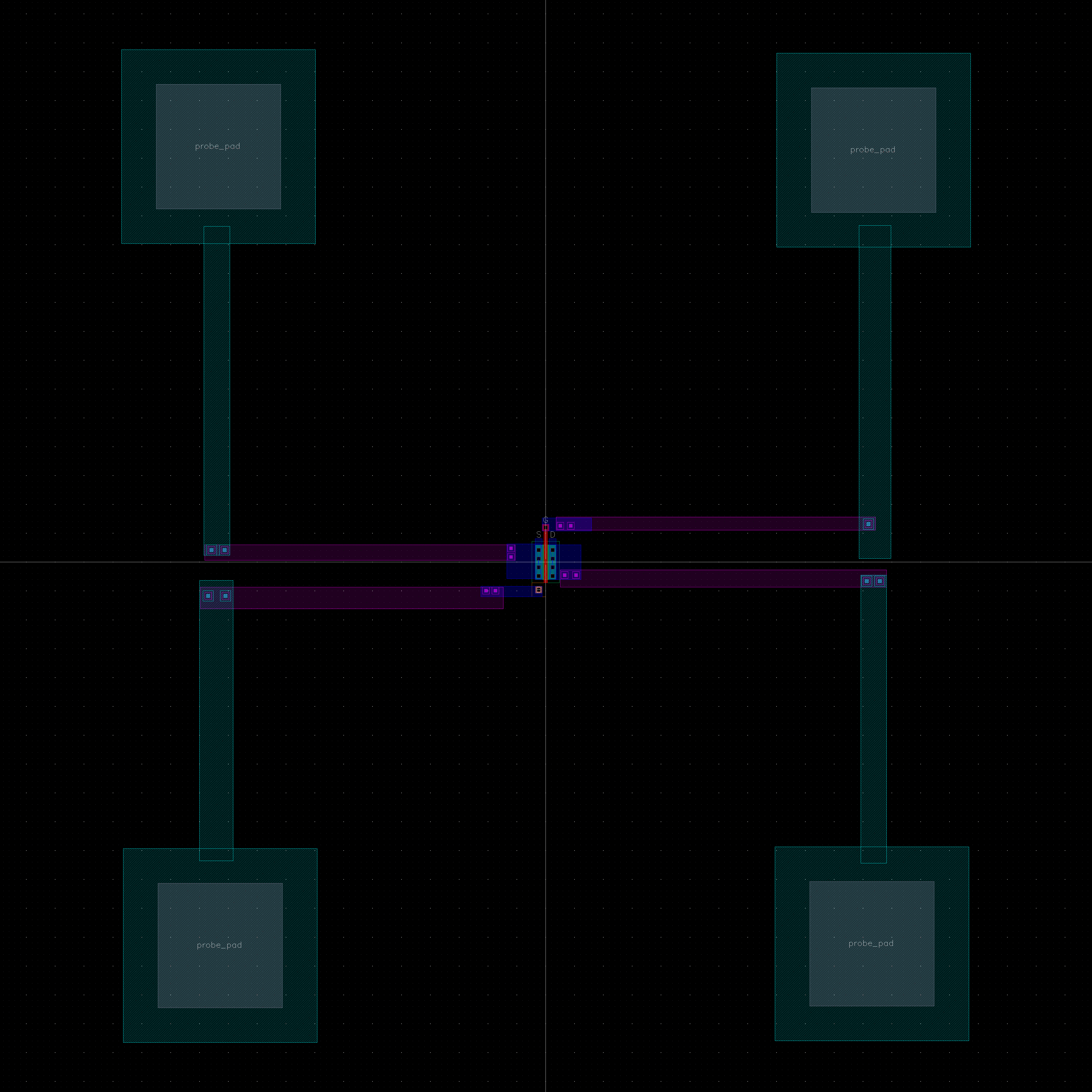
The layout of an NMOS transistor device can be seen below.
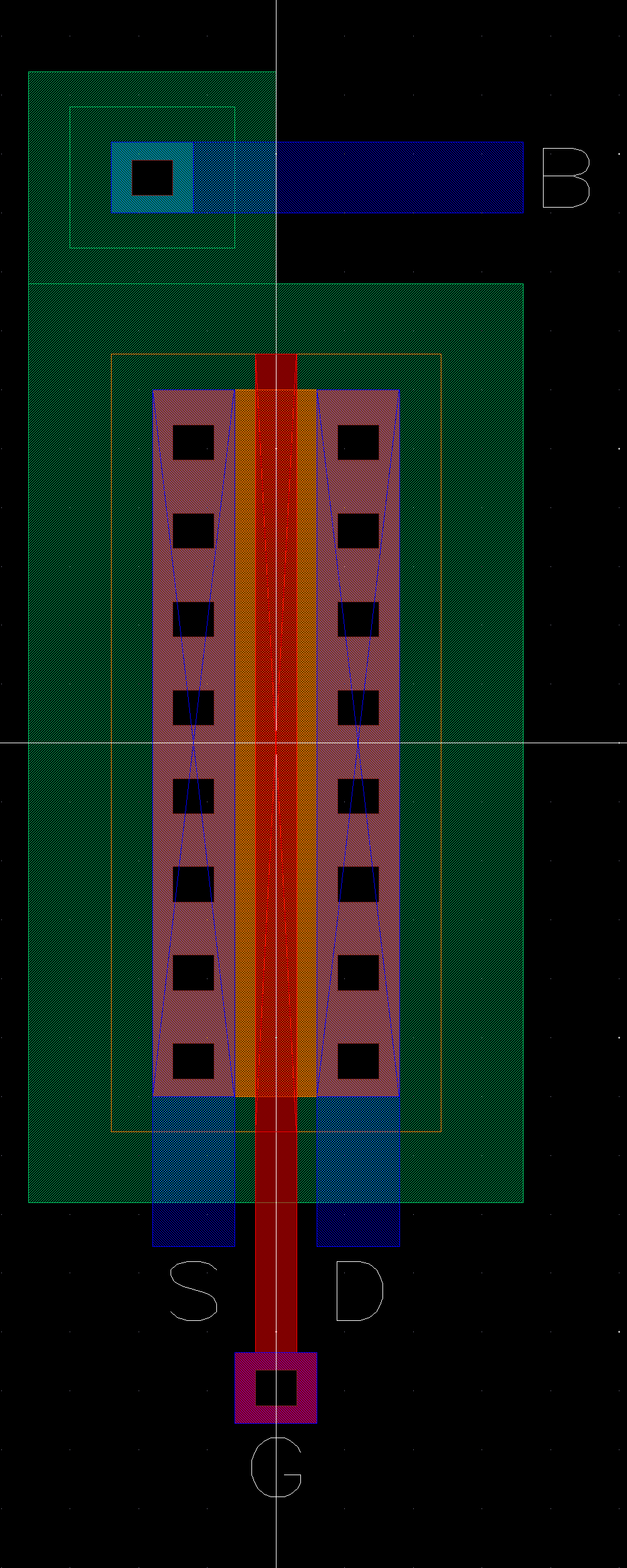
The layout of an PMOS transistor device can be seen below.
Lab
Generating Schematics and Simulations
We start off by characterizing the transistor devices we will be working with.
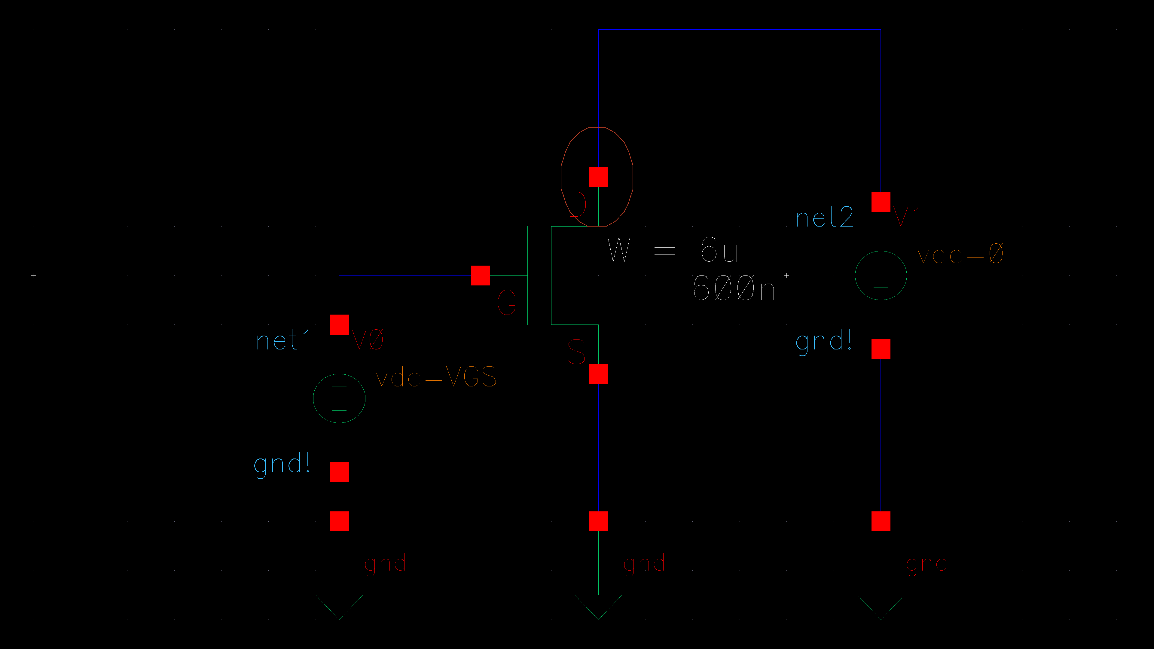
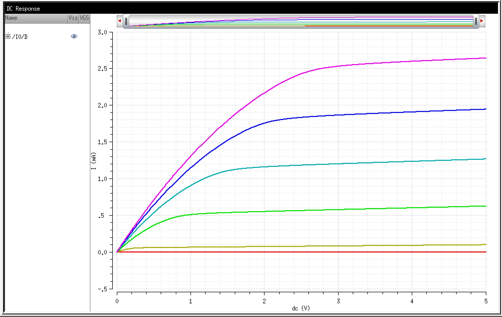
ID v. VDS of a NMOS
Here, we vary VGS from 0 to 5V in 1V steps while VDS varies from 0 to 5V in 1mV steps.
Note: A 4 terminal device can be used, connecting the body to the source. The 3 terminal NMOS has this already done internally.
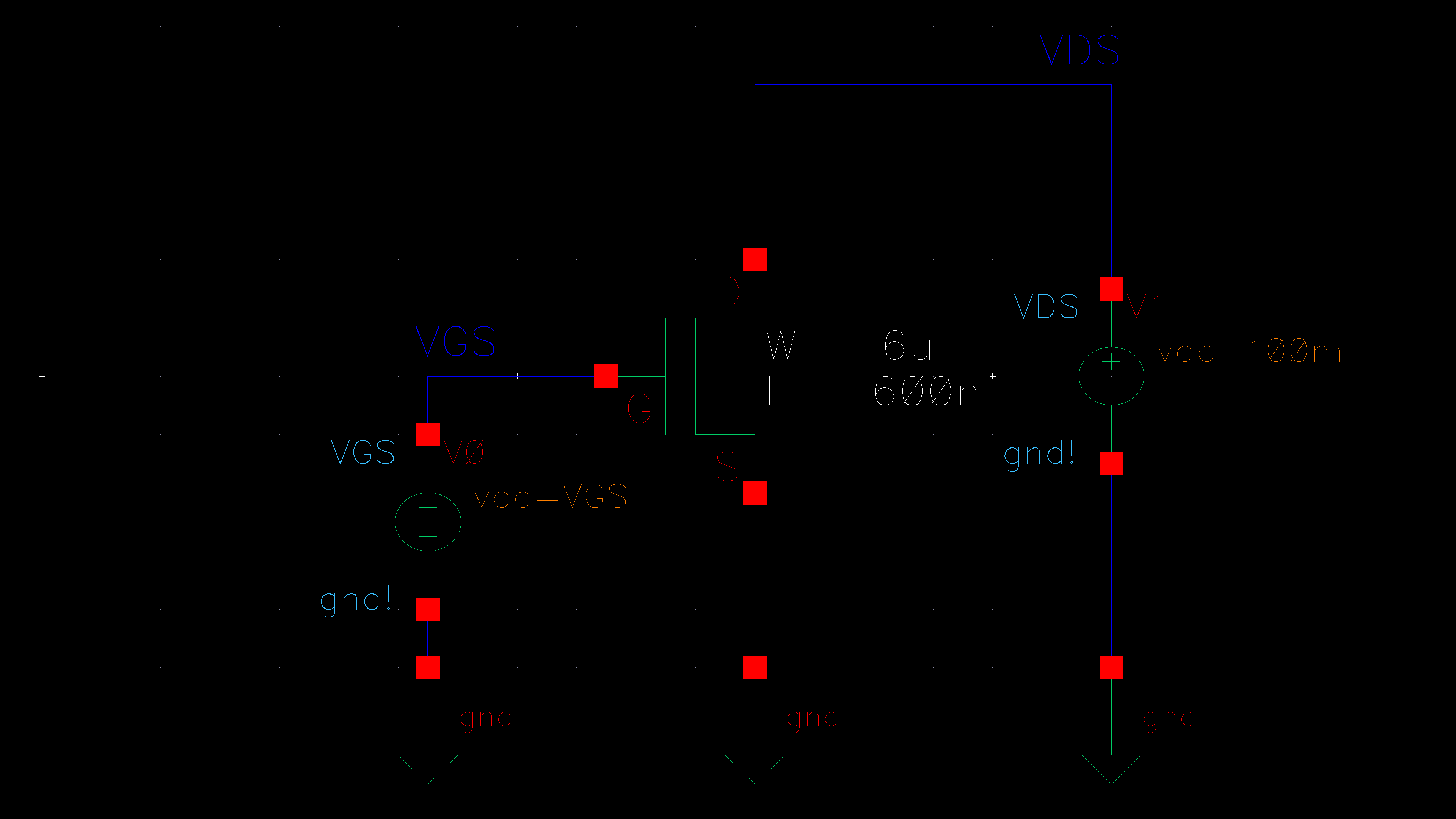
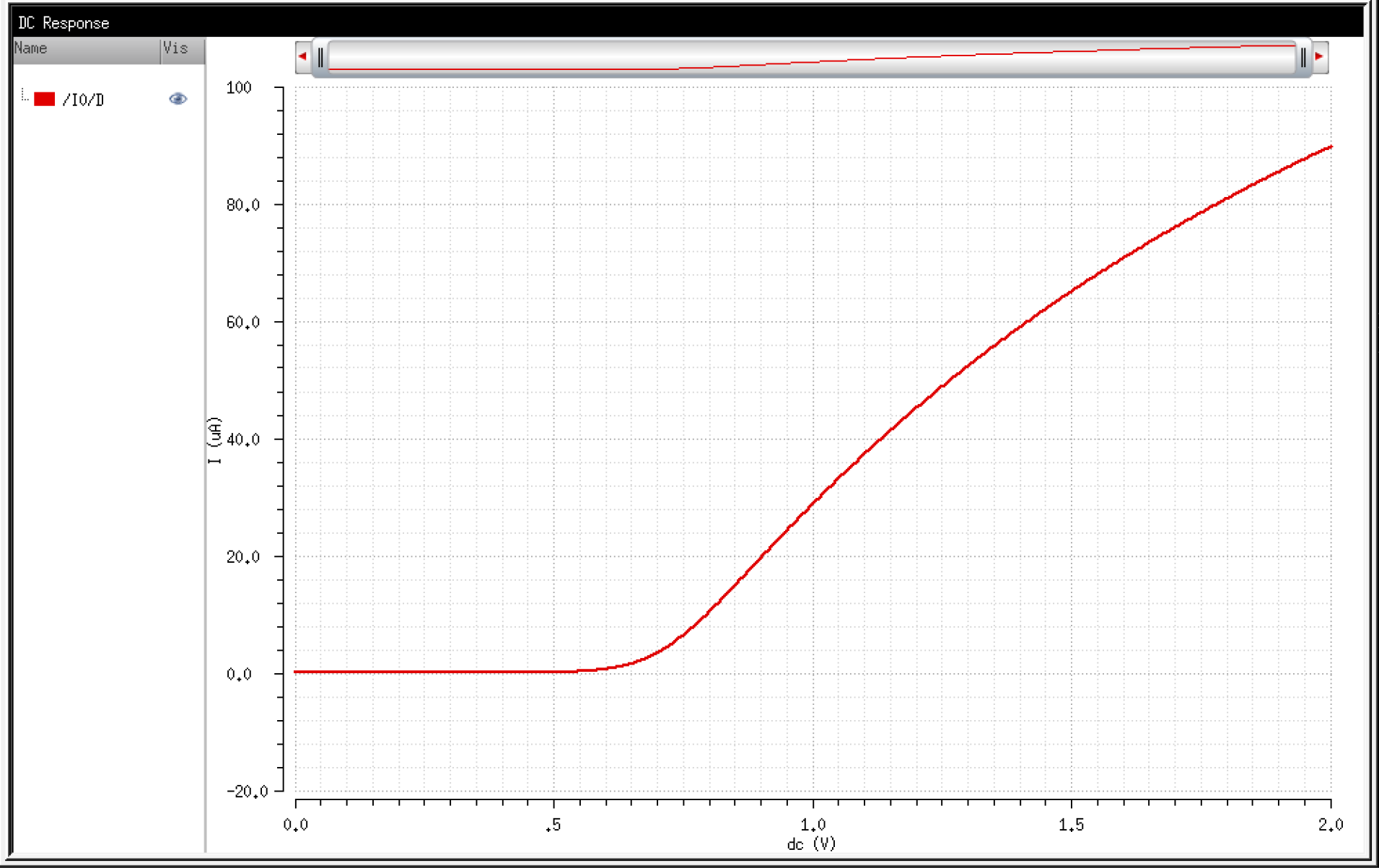
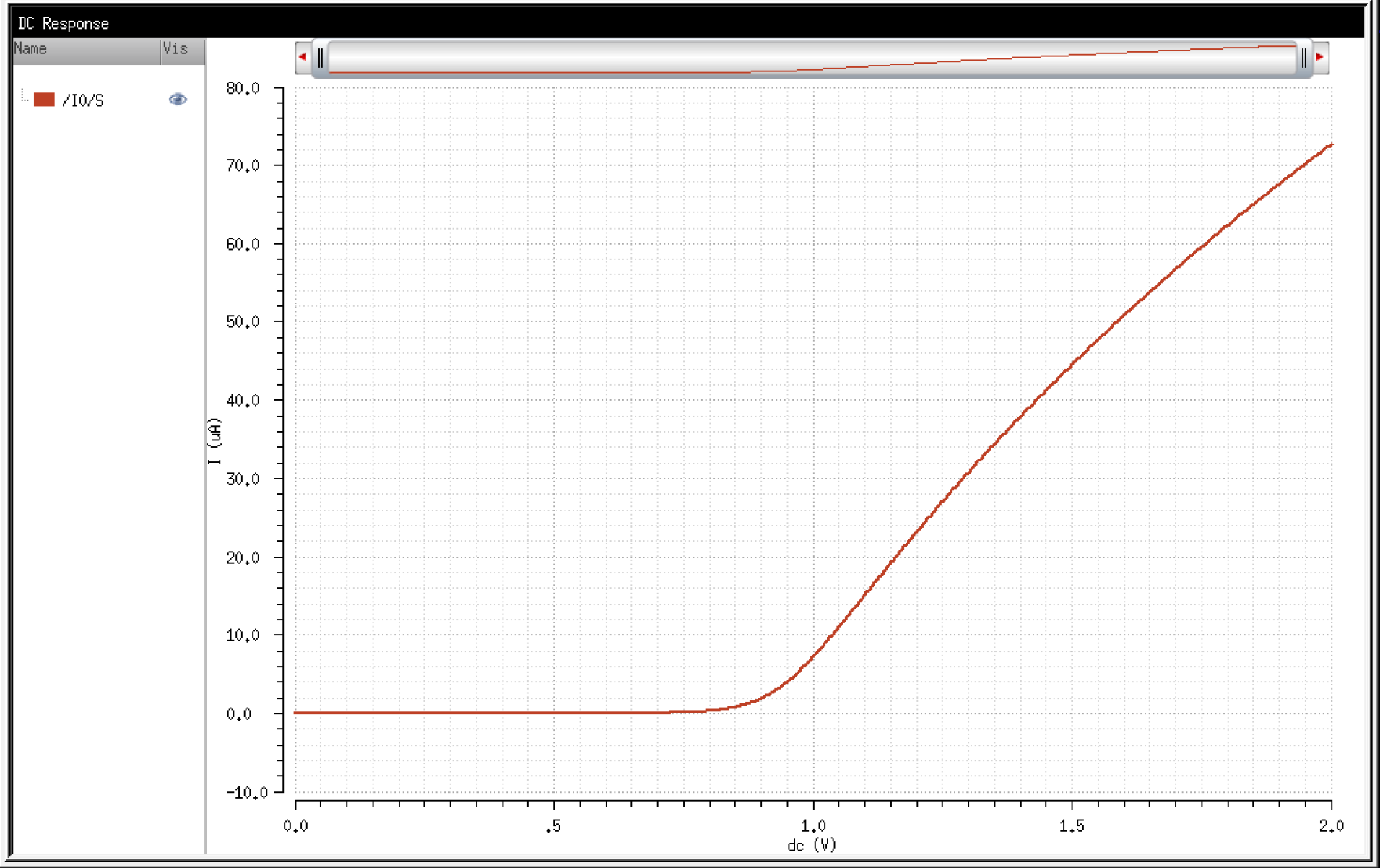
ID v. VGS of a NMOS
Here, we set VDS = 100mV and vary VGS from 0 to 2V in 1mV steps.
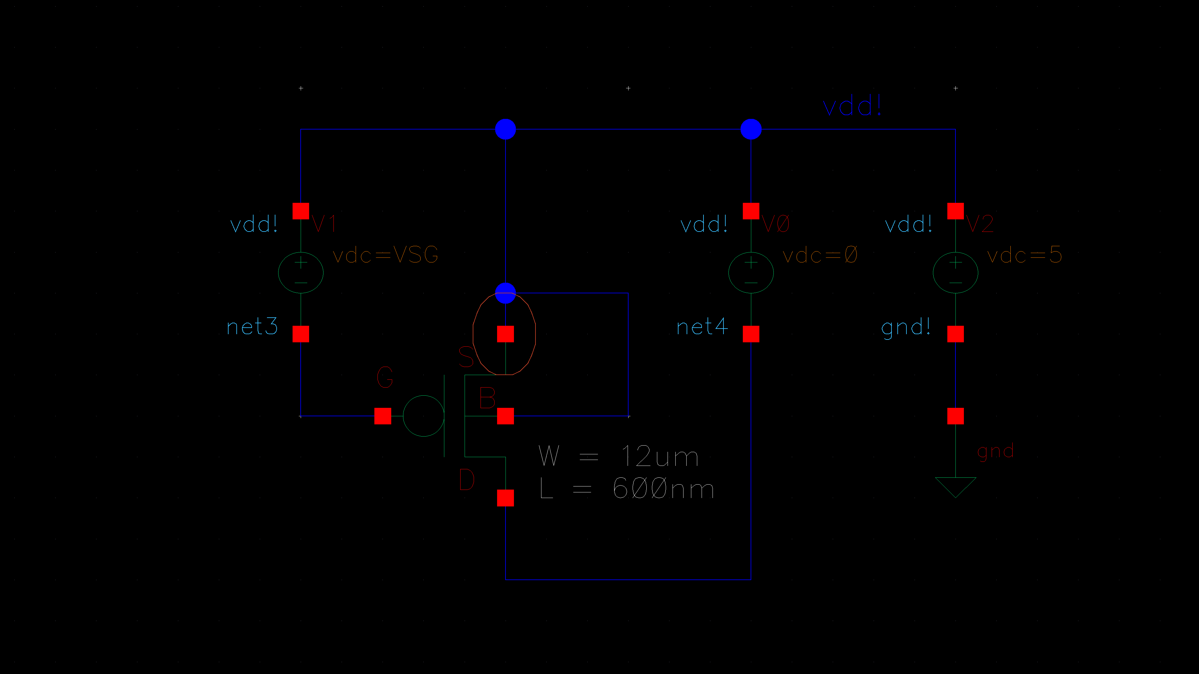
ID v. VSD of a PMOS
Here, we vary VSG from 0 to 5V in 1V steps while VSD varies from 0 to 5V in 1mV steps.
ID v. VSG of a PMOS
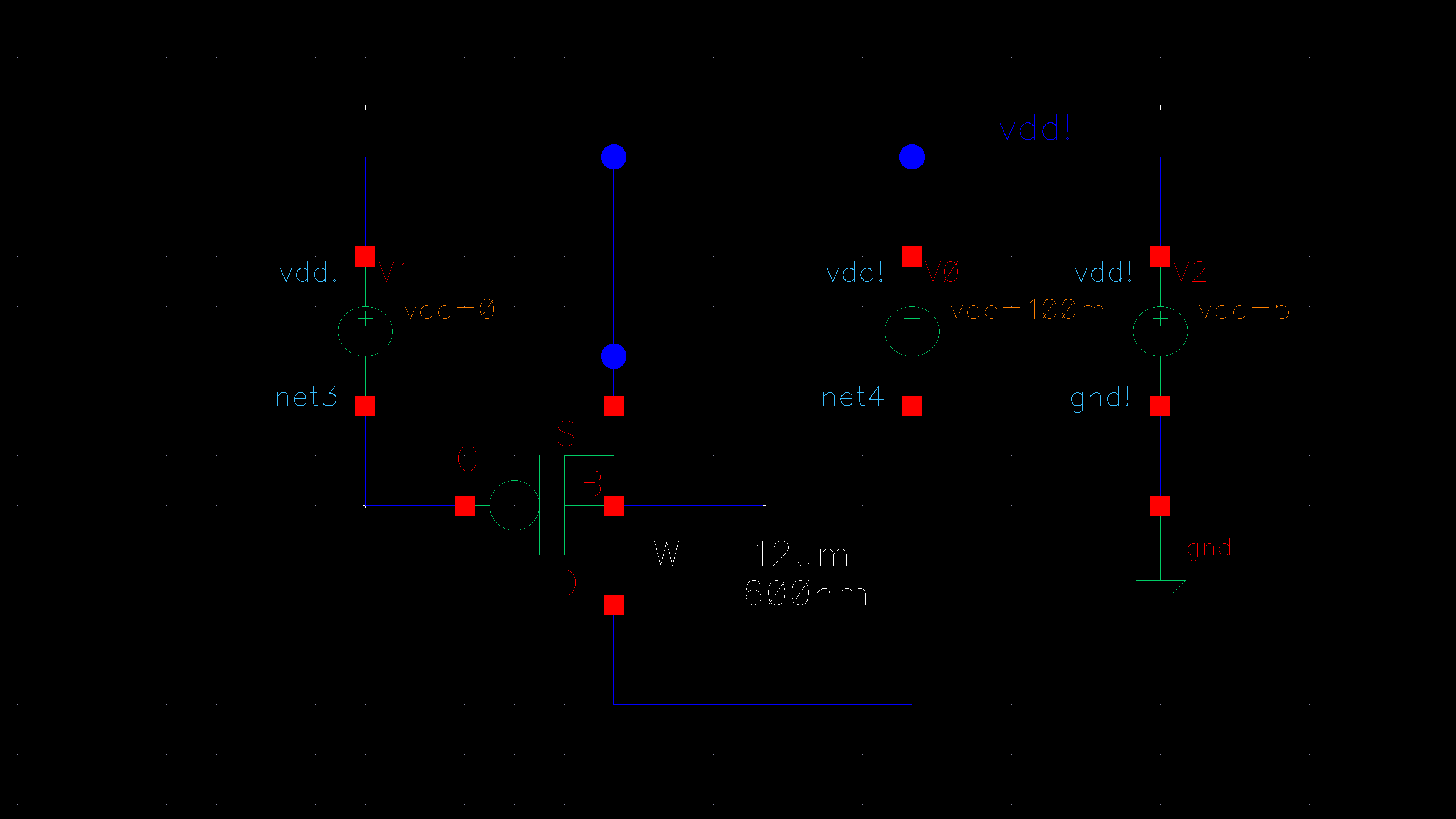
Here, we set VSD = 100mV and vary VSG from 0 to 2V in 1mV steps.
Note: The body of the PMOS should be connected to VDD.
Generating Schematics and Simulations
Now
we can layout our transistor devices. We will connect the terminals to
probe pads. Probe pads can be used after fabrication to test the real
operation of the design.
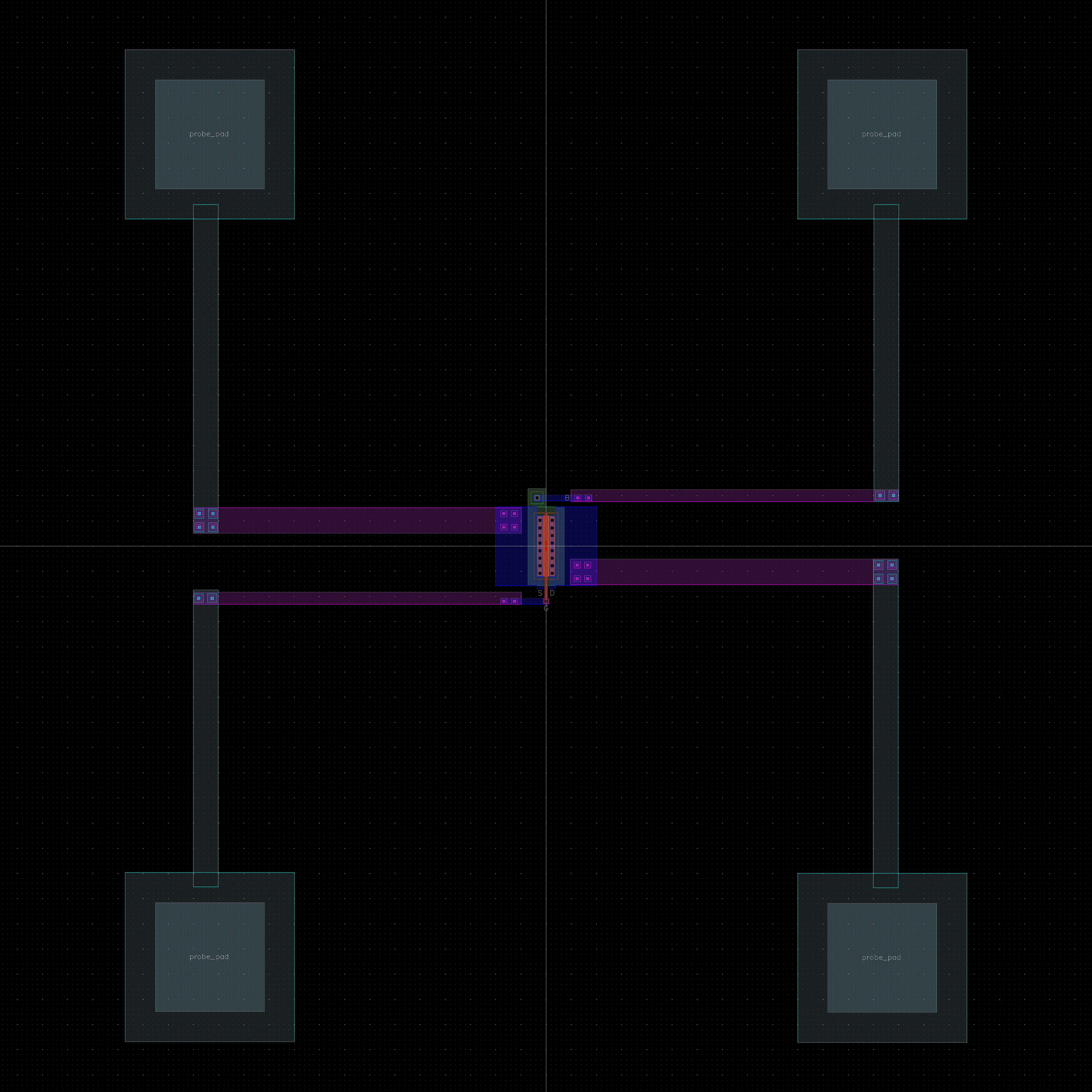
We start with the NMOS.
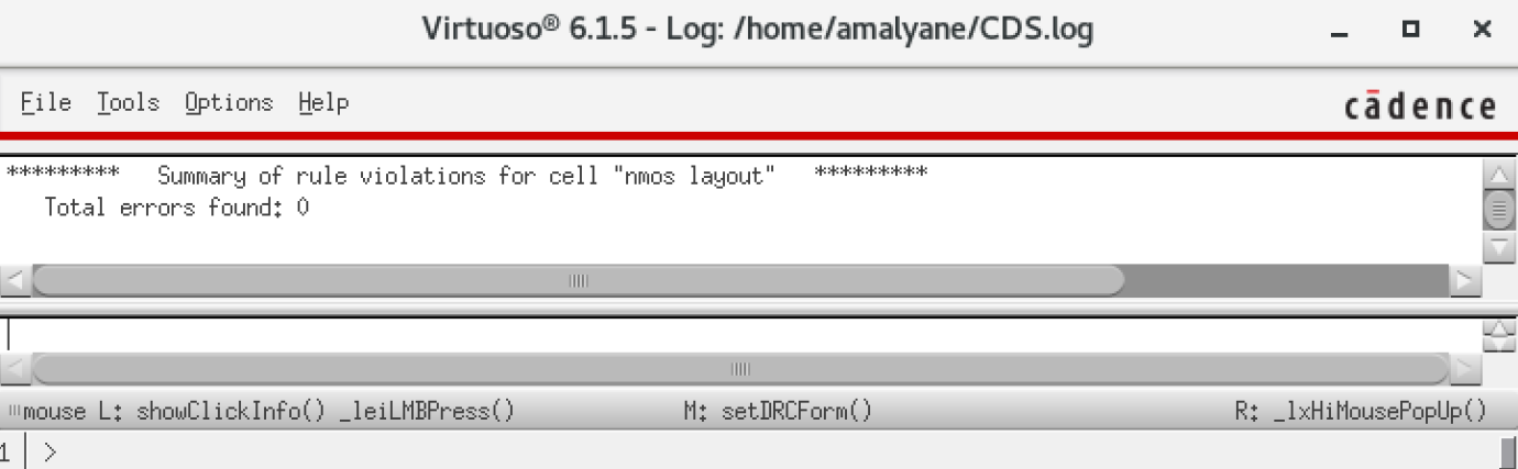
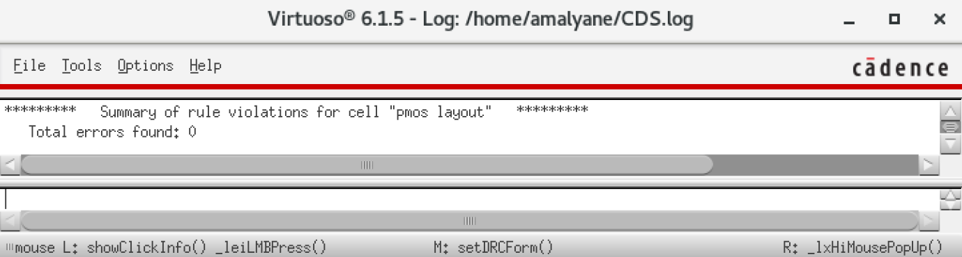
We run the DRC. Metal layers and vias should be appropriately spaced from each other.
We extract the layout.
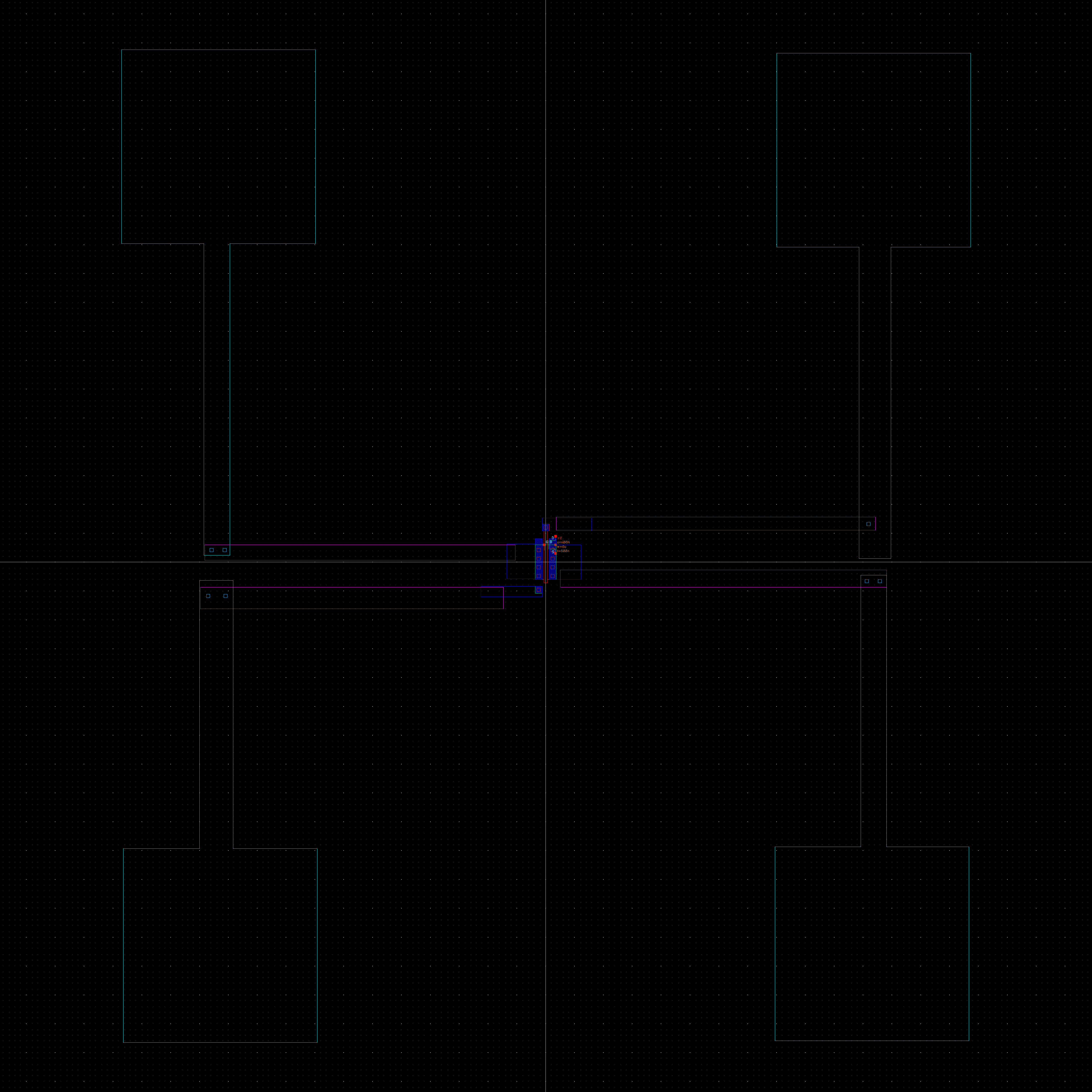
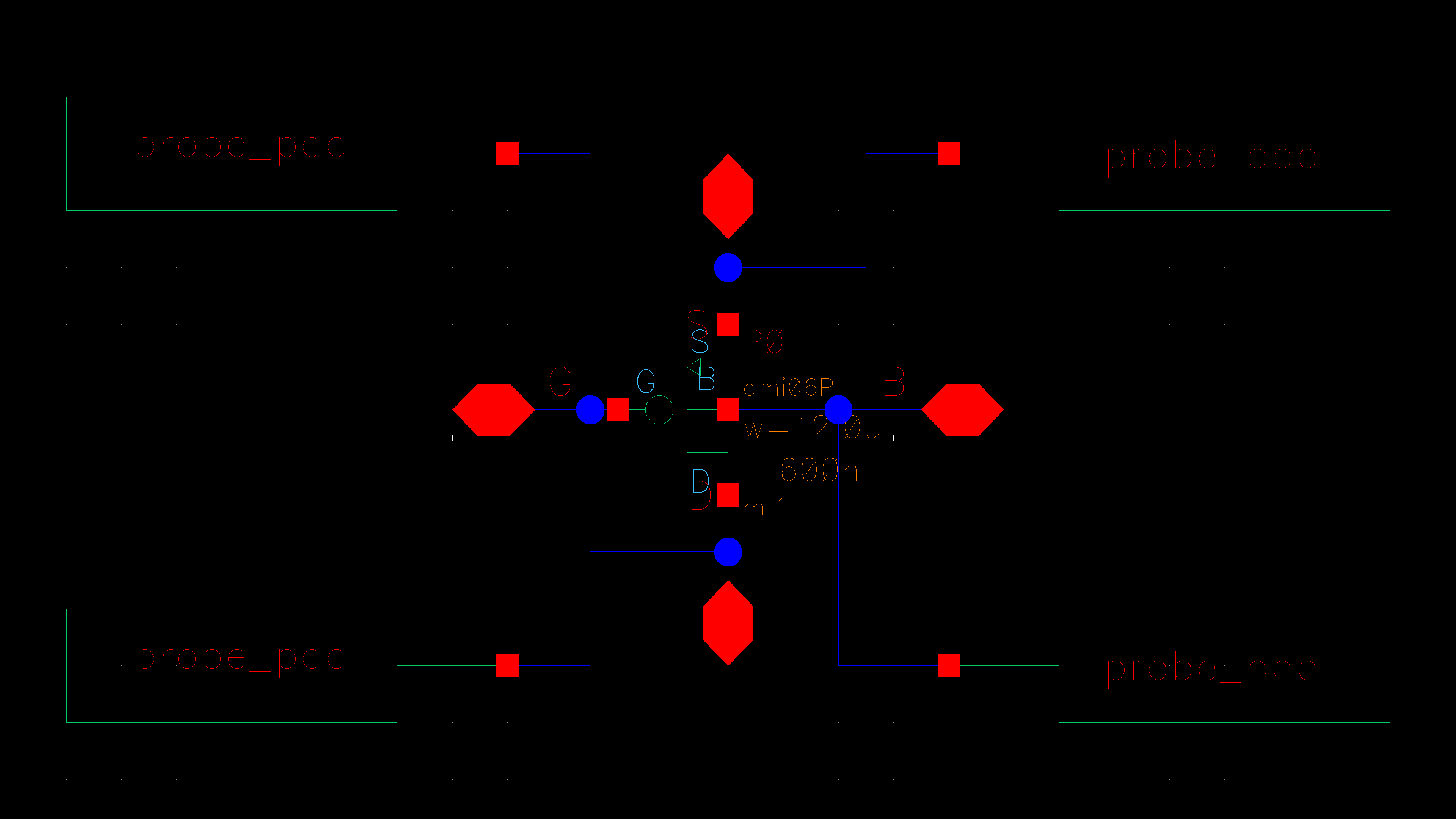
We create a schematic (4-terminal device).
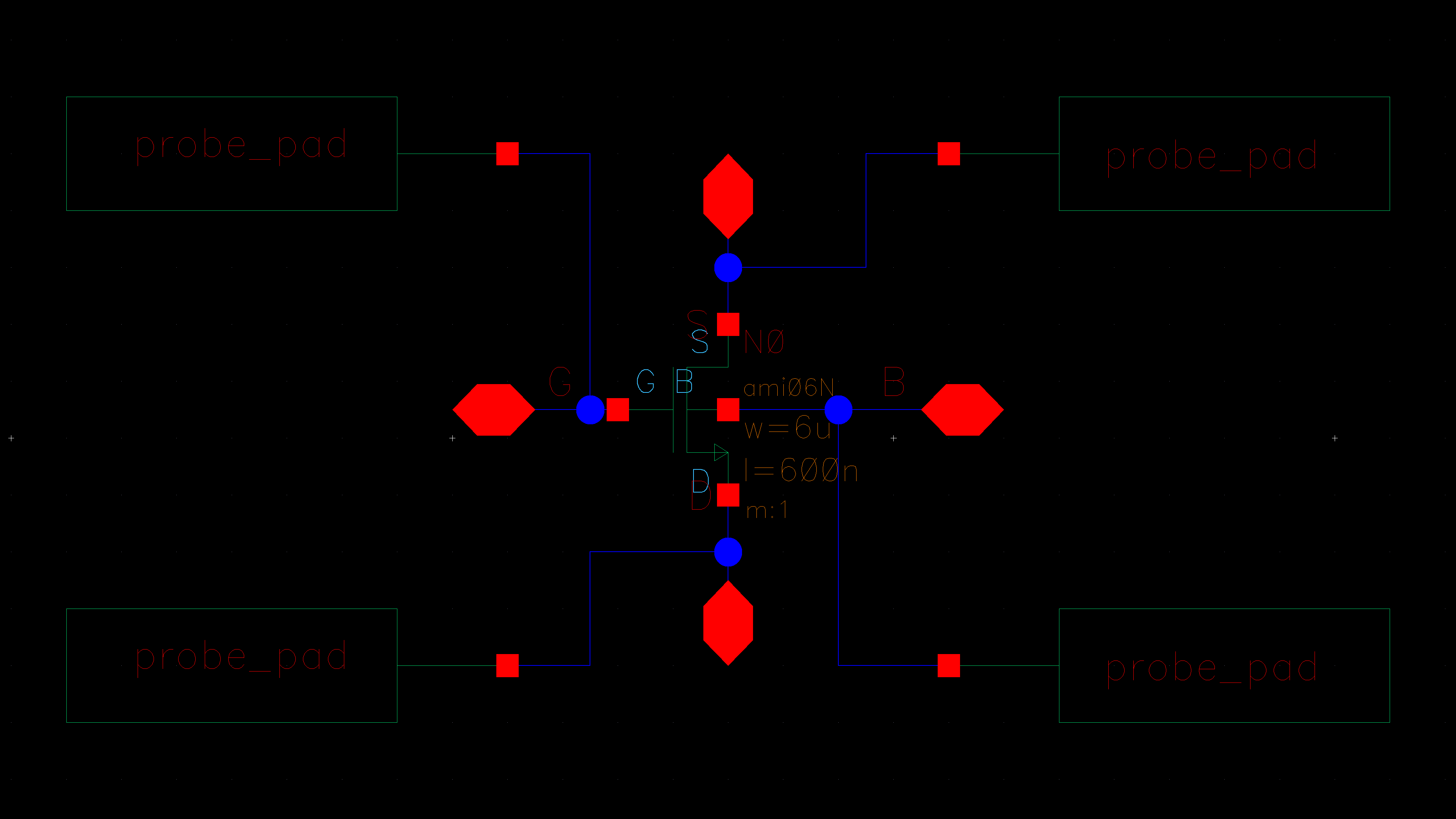
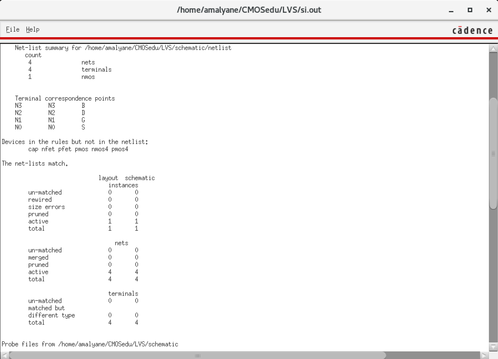
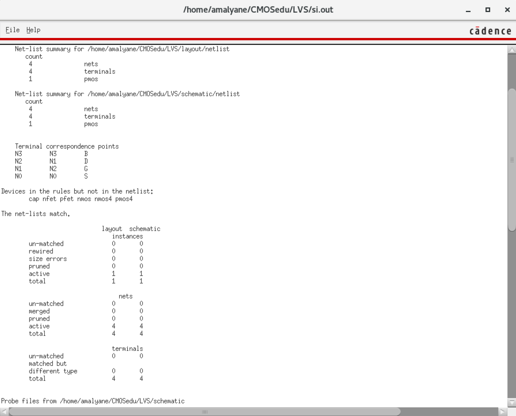
We run the LVS.
Next is the PMOS.
We run the DRC. Metal layers and vias should be appropriately spaced from each other.
We extract the layout.
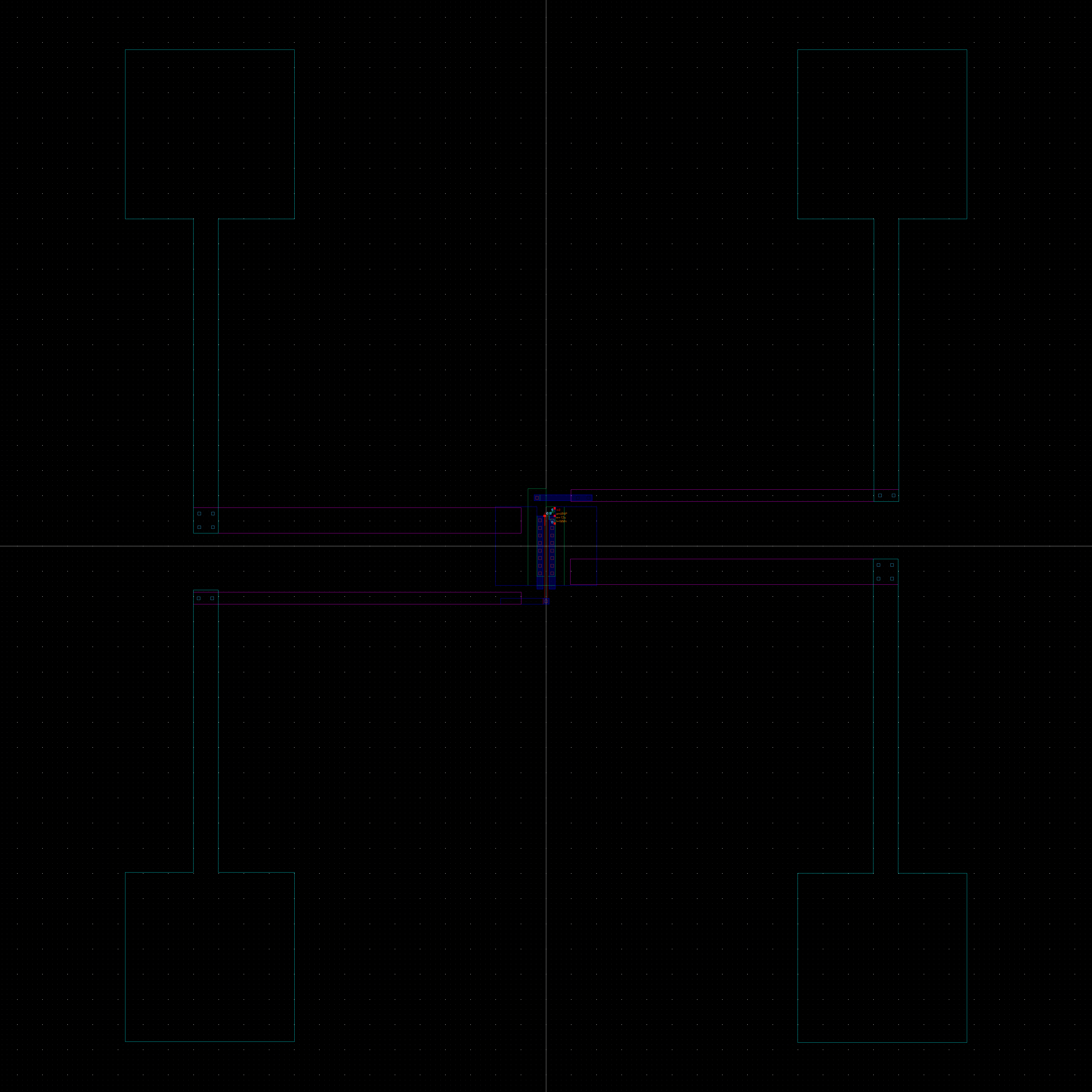
We create a schematic (4-terminal device).
We run the LVS.
Backups:
As
demonstrated in Lab 1, I run ./backup.sh from the Cadence server and
download the 'Backup' folder containing the compressed archives of my
CMOSedu and entire home directories.
All files pertaining to this lab report already exist and are directly edited from another folder that also gets synced.
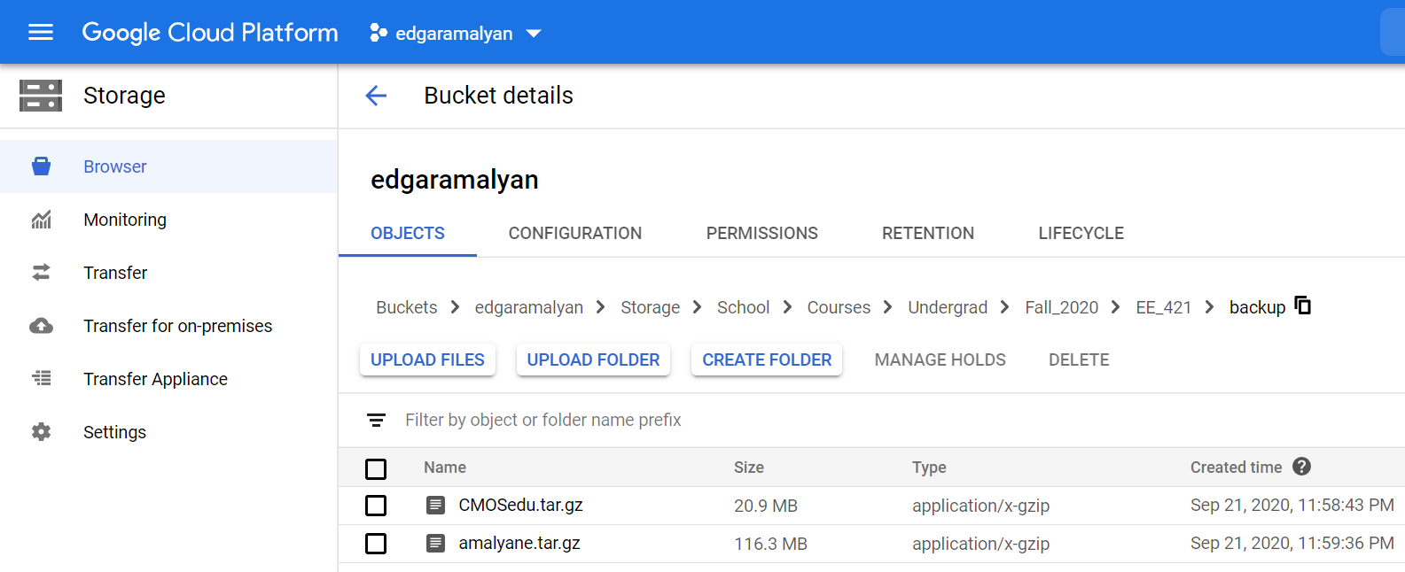
I run sync_to_gcp.bat from my computer which makes my GCP Storage bucket identical to my local directory.

Return to EE 421L Labs