Lab 3 - EE 421L
Author: Edgar Amalyan
Email: amalyane@unlv.nevada.edu
Date: 09/16/2020
Goals:
This lab focuses on the layout of the 10-bit DAC created in Lab 2.
Prelab
Note: Click on pictures for larger views.
Tutorial 1
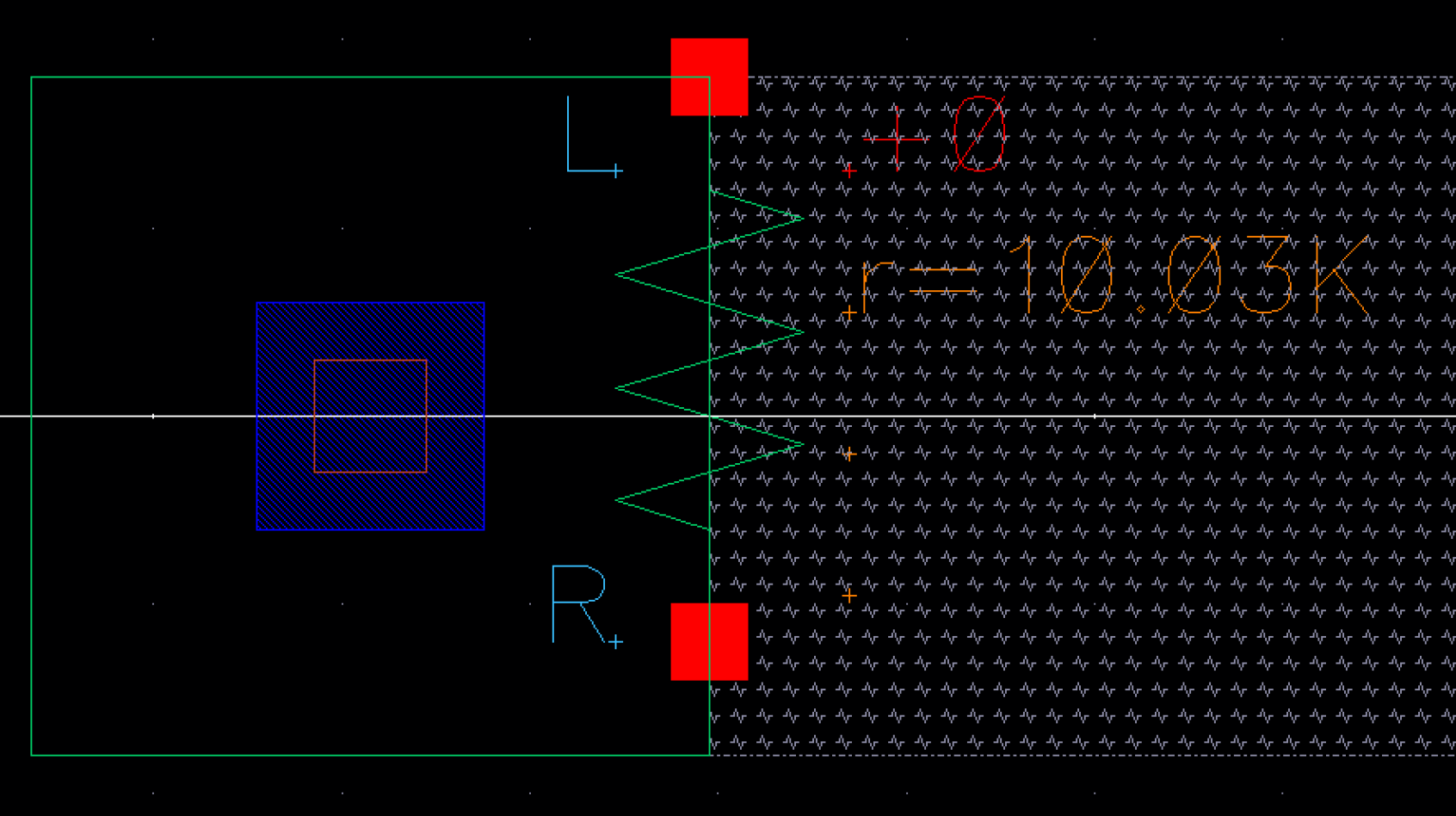
The extracted view my n-well resistor can be seen below. A resistance of 10.03kΩ can be seen.
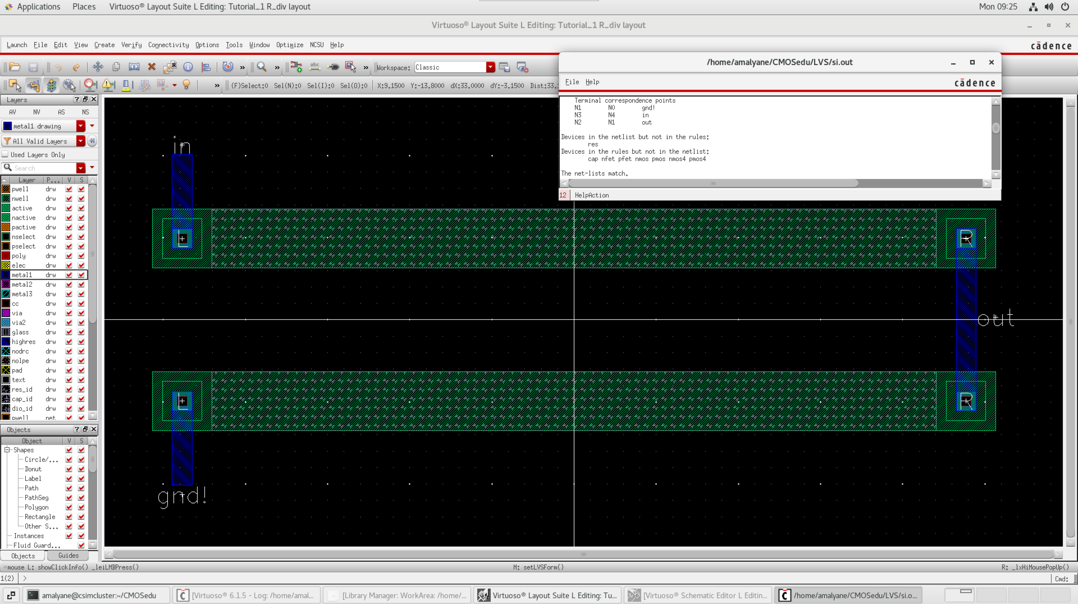
The layout with the LVS check can be seen below.
Lab
Selecting Width and Length of Resistor
The
equation, R = Rsquare * (l/w) relates the specifications of our
resistor. The Rsquare value used by Cadence for our C5 process can be
found by laying out a resistor (following the rules of the process) and
observing the resulting resistance. For example, we can use an Rsquare
value of 855, which is given in the C5 data sheet. If we want a 10k
resistor, using a width of 3.6um, we will need a length of 42.1um. We
layout a resistor with these specifications and view the resulting
resistance in the extracted view. The resistance that will be seen will
not be exactly 10k. This means that the Rsquare value was not exactly
855. If we plug the resulting resistance, the width, and the length we
used back into the equation, and solve for Rsquare, we find the a much
more accurate value of Rsquare that was used by Cadence. This value is
around 819 Ω/square. This will be the value we use.
As
stated in Tutorial 1, the minimum width of n-well is 12 lambda, where
lambda is 300nm. The minimum width resulted is 3.6um. We will use this
value as our width. Note
that this width can be increased, to for example 4.5um, just not
decreased below 3.6. Our equation becomes 10000 = 819 * (l / 3.6u), so
solving for l yields 43.956um. We can divide this by 2 so we have 2
equal halves in our layout for ease of design purposes. To follow the
design rules, the length should be a multiple of 0.15um. Creating a
ruler automatically snaps the spacing to 0.15um steps. The two closest
lengths that are multiples of 0.15 are 21.9 and 22.05. Our value of
43.956 / 2 = 21.978 is closer to 22.05, so we will 22.05 as our length
for each half of the resistor. A resistance of 10.03k is acheived as
shown in the prelab.
Layout
Now
that we have completed the DRC of our 10k n-well resistor, we can use
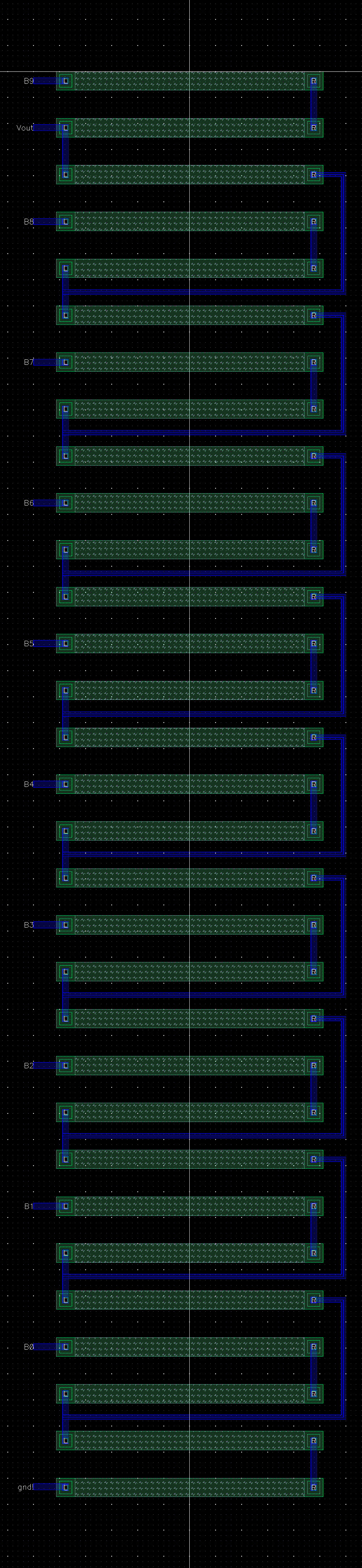
it to build our DAC. The DAC is simply ten 1/3 voltage dividers
connected together. Each one of these voltage dividers is essentially a
1-bit DAC consisting of three 10k resistors. We have to perform the
layout of this circuit. We start by instantiating three of the n-well
resistors that we just created the layout for. Note
that we should use the layout and not the extracted file when inserting
the component. Per the design rules, the resistors should be 5.4um
apart from each other in the vertical direction. We make sure that all
the resistors line up in the horizontal direction. Now that we have
positioned them physically, we can create the pins and connections. We
can open the schematic for our DAC to help us remember names and how
everything was connected. We can picture every 3 resistors as a group,
or a 1-bit DAC. The first resistor has an input of B9. This resistor is
connected to the second resistor. The end of the second resistor is
Vout and is also connected to the third resistor. The third resistor
should be connected to the end of the second resistor in the second
group. The first resistor in the second group again has an input that
we name B8. This time, we do not need a Vout terminal. Once again, the
end of the third resistor in the second group is connected to the
second resistor in the third group, and so on. We make sure to draw all
the pins and connections in the metal layer. The connections between
two adjacent resistors can be created by a simple rectangle. To make
our layout look nicer, we can use the create path tool to connect the
last resistor in each group to the second resistor of the next group.
To discontinue the drawn path, press enter on the keyboard. Now that we
have essentially what the entire layout will consist of, we can just
copy and paste the resistors and connections until we reach the last
resistor of the group that features B0 as the input. The end of the
this last resistor simply goes to just one other resistor, which is
then terminated to ground. Note
that rulers are very helpful in keeping the layout clean and organized,
which ultimately makes the entire process more efficient.
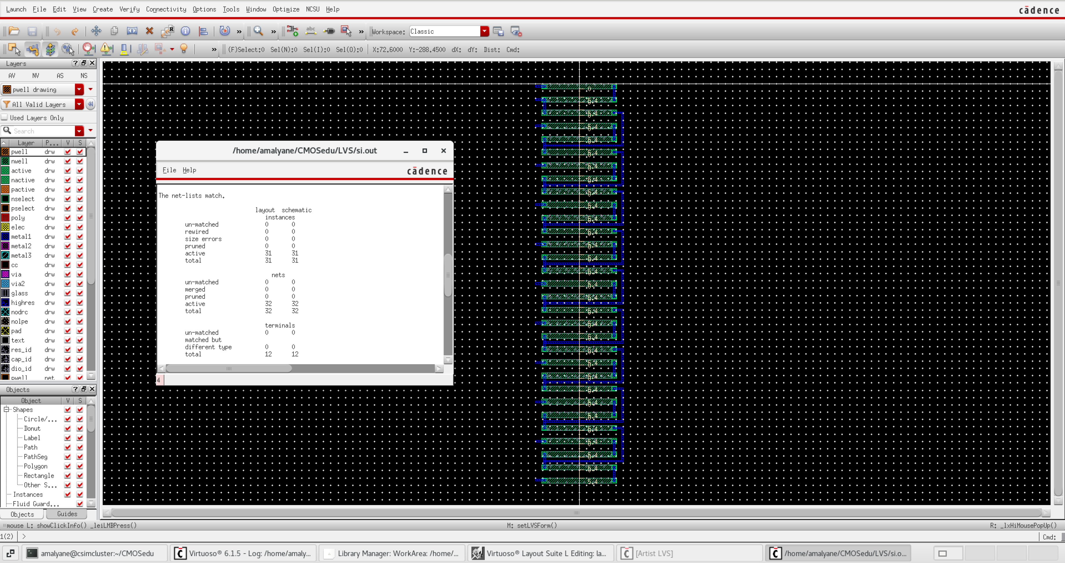
Now
that our layout is finished, we make sure we pass the DRC. After, we
can extract the view, and run the LVS. The LVS will make sure our
layout matches the schematic of our 10-bit DAC.
Design Files
Attached here is the zipped directory of lab 3.
Included
is the schematics and symbols of the 1-bit and 10-bit DACs, the layout
and extracted views of the 10k n-well resistor and 10-bit DAC, and the
schematic and simulation state of the ADC+DAC circuit.
Backups:
As
demonstrated in Lab 1, I run ./backup.sh from the Cadence server and
download the 'Backup' folder containing the compressed archives of my
CMOSedu and entire home directories.
All files pertaining to this lab report already exist and are directly edited from another folder that also gets synced.
I run sync_to_gcp.bat from my computer which makes my GCP Storage bucket identical to my local directory.
Return to EE 421L Labs