Lab 6 - ECE 421L
Authored
by Geovanni Portillo,
October 19th, 2019
Design, layout, and simulation of a CMOS NAND gate, XOR gate, and Full-Adder
All images can be double-clicked to view larger versions
Lab 6 files can be downloaded here or at the bottom of the page
Prelab:
- Back-up all of your work from the lab and course
- Go through Cadence Tutorial 4
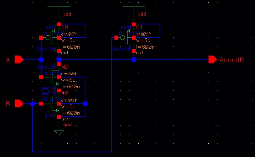
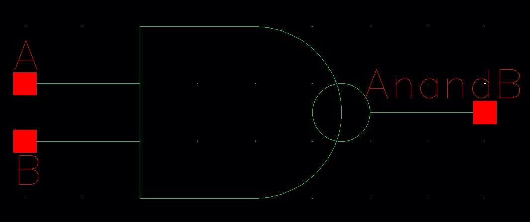
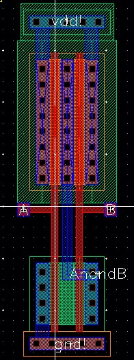
| NAND 2 Input |
| Schematic | Symbol | Layout | Extracted |
 |  |  |  |
| LVS |
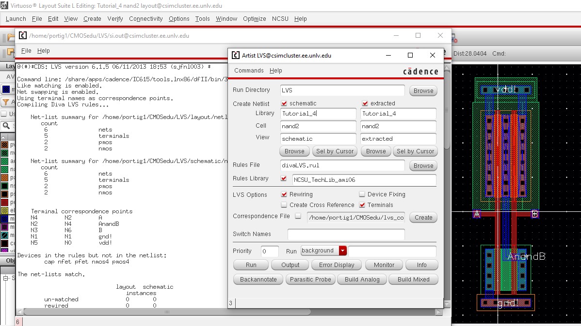 |
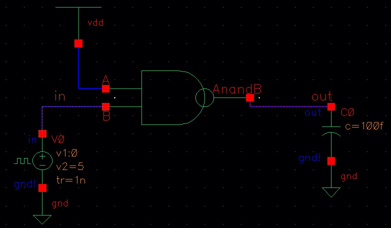
| NAND 2 Input Simulation |
| Schematic | Plot |
 | 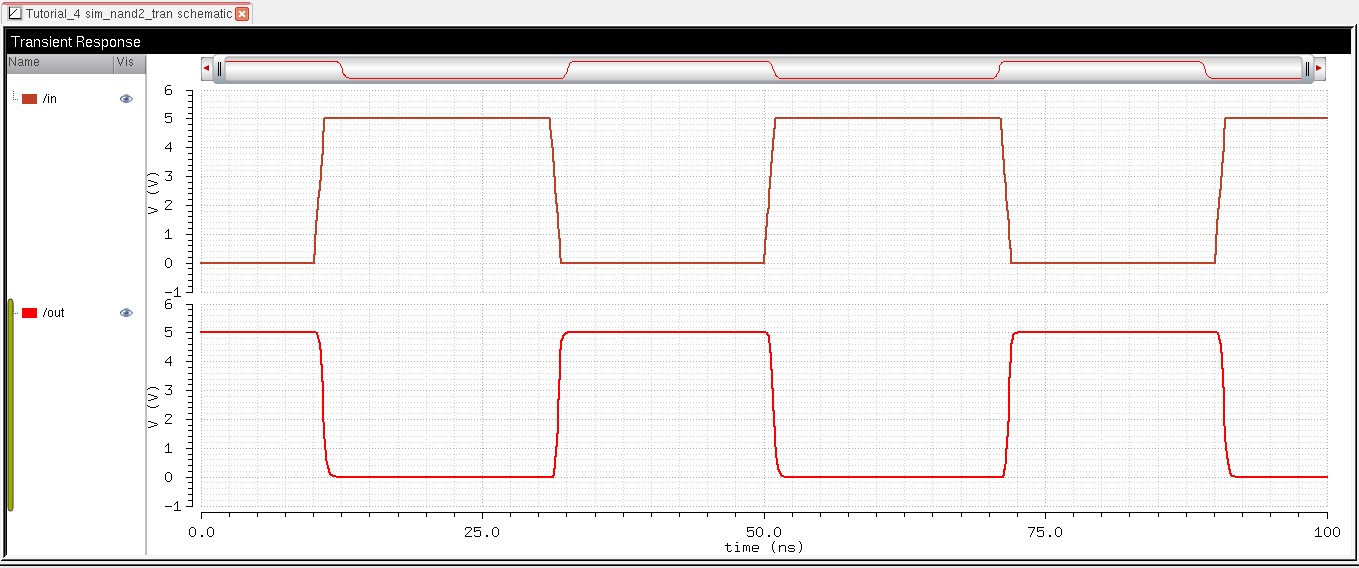 |
Lab:
Draft
the schematics of a 2-input NAND gate (Fig. 12.1), and a 2-input XOR
gate (Fig. 12.18) using 6u/0.6u MOSFETs (both NMOS and PMOS)
| NAND |
| Schematic | Layout |
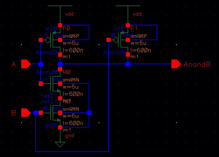 | 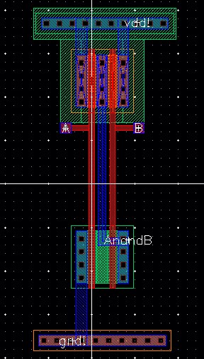 |
| Extracted | Symbol |
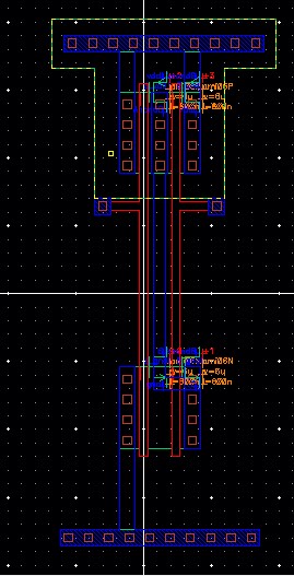 | 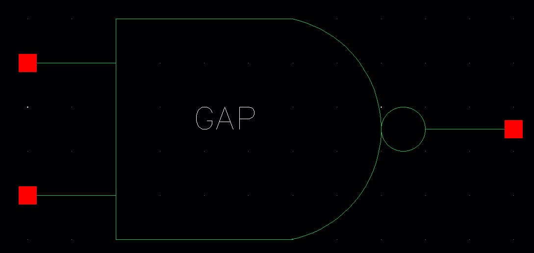 |
| DRC | LVS |
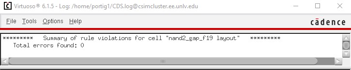 | 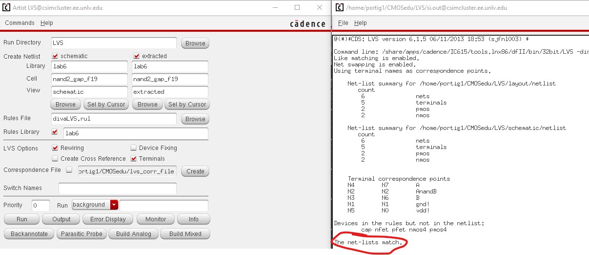 |
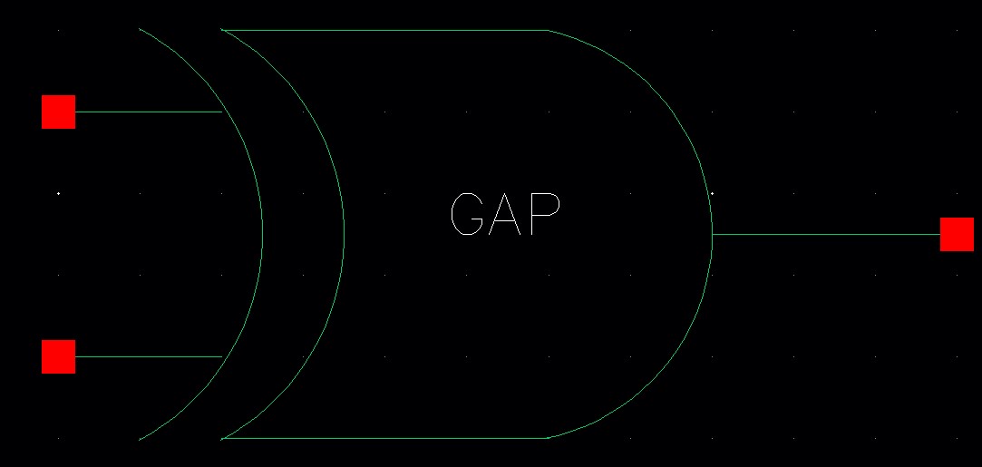
| XOR |
| Schematic | Layout |
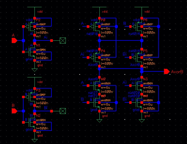 | 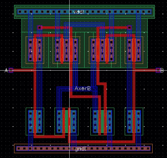 |
| Extracted | Symbol |
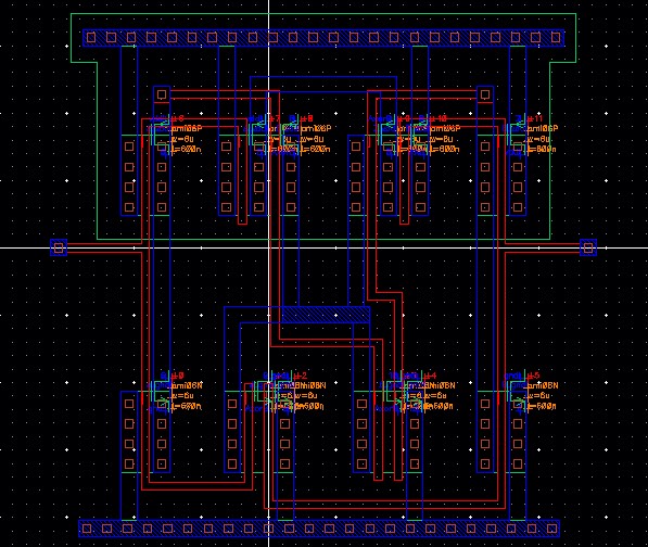 |  |
| DRC | LVS |
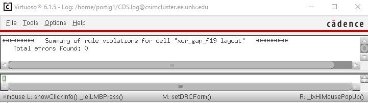 | 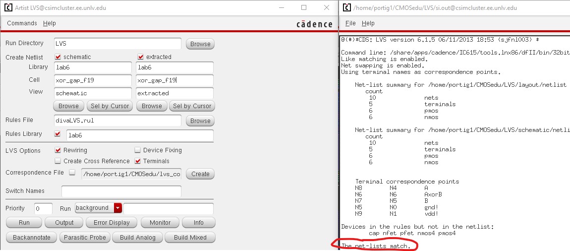 |
Using Spectre simulate the logical operation of the gates for all 4 possible inputs (00, 01, 10, and 11)
| Schematic | Plot |
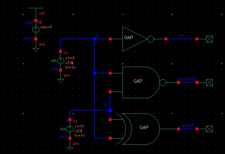 |  |
We
can see that the inverter, nand and xor gates are operating as
expected. Though, the xor gate shows glitches when we go from A'B to
AB' since the transition between the inputs isn't instant. If the
rise/fall times aren't fast enough the output can show a different
behavior for a brief period of time, as we see in the xor waveform. One
method of resolving this would be to have an even number of inverters
so on the inputs so that when there is a change, the rise/fall times
will be quick enough.
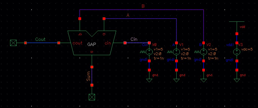
Using these gates, draft the schematic of the full adder. Create a symbol for this full-adder.
Simulate, using Spectre, the operation of the full-adder using this symbol. DRC and LVS your full adder design.
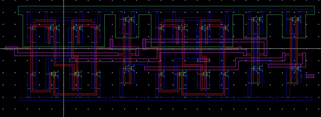
| Full Adder |
| Schematic | Layout |
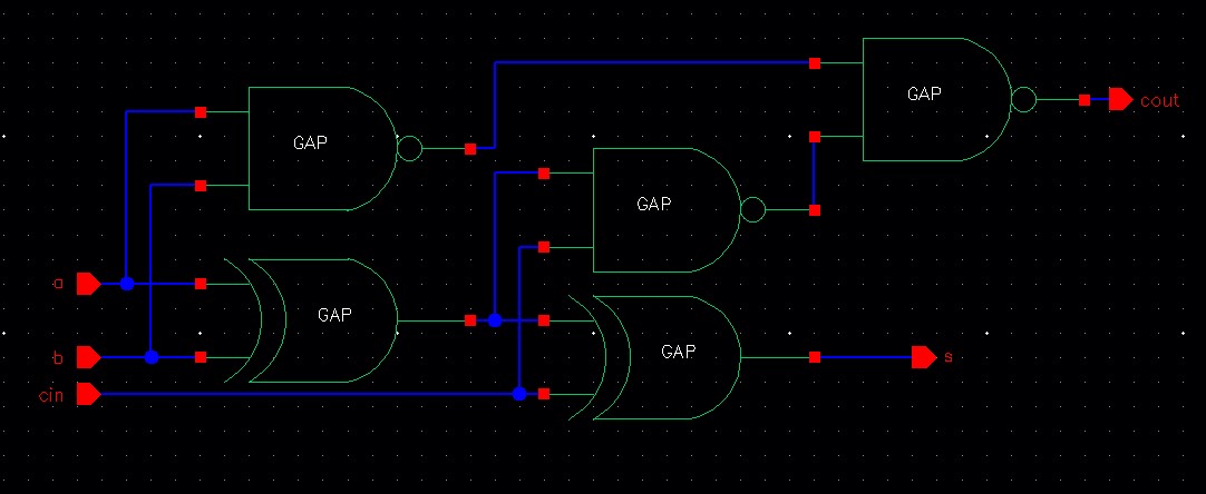 | 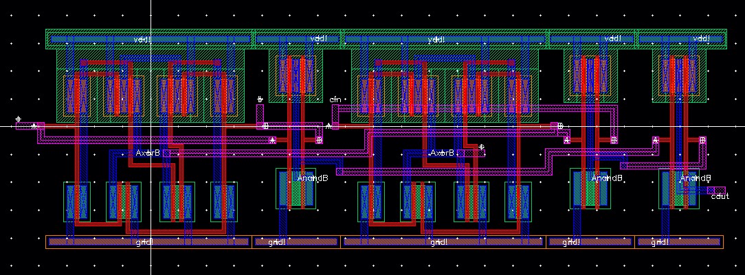 |
| Marked up layout view to point out pins |
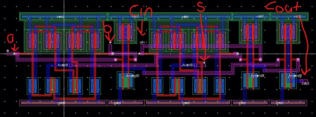 |
| Extracted | Symbol |
 | 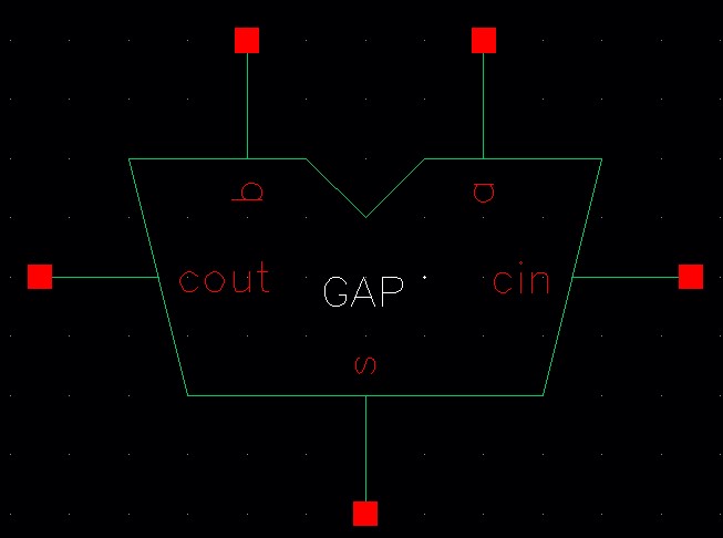 |
| DRC | LVS |
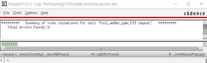 | 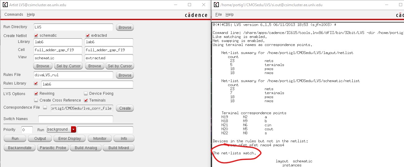 |
Simulate, using Spectre, the operation of the full-adder using the symbol
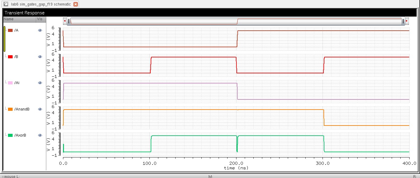
| Full Adder Simulation |
| Schematic | Plot |
 | 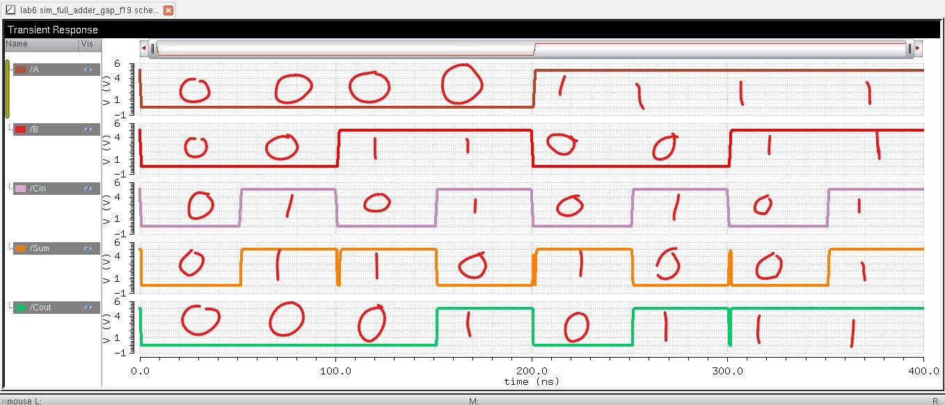 |
The output matches what is expected of a full adder.
Design files and lab reports are backed up to October 18th, 2019
Files for lab6 can be downloaded here or at the top of the page
Return to Index
Return to EE 421 Labs