Lab 4 - ECE 421L
Authored
by Geovanni Portillo,
September 16th, 2019
portig1@unlv.nevada.edu
IV characteristics and layout of NMOS and PMOS devices in ON's C5 process
Prelab:
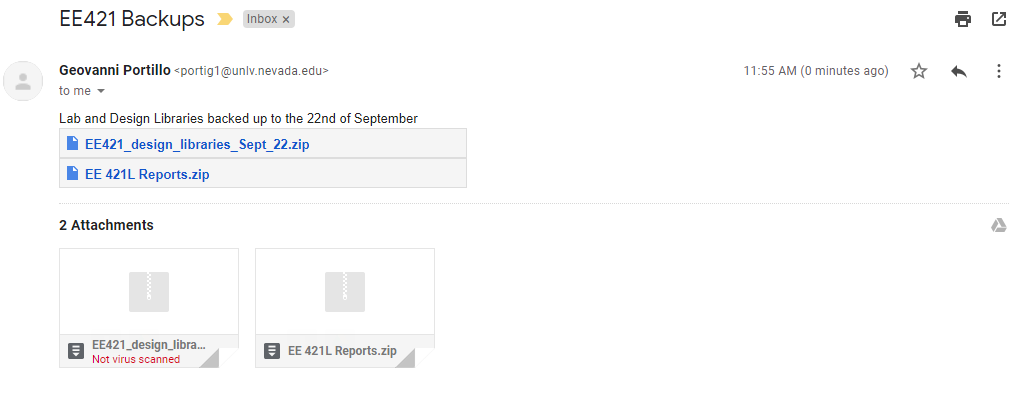
- Work from labs and course is backed up via email
- Tutorial
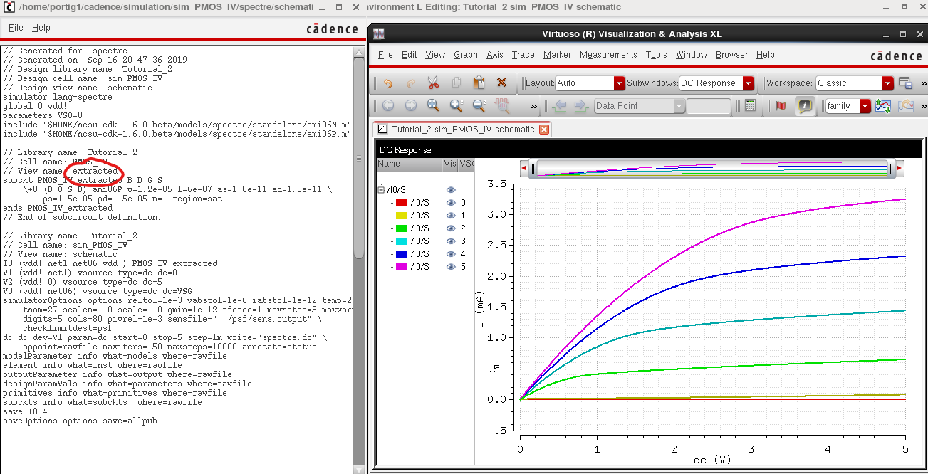
2 goes through modeling the schematic and layout of NMOS and PMOS as
well as simulating the circuits and plotting their IV curves
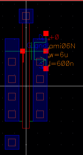
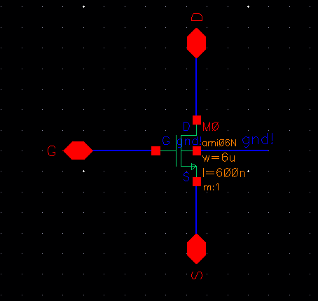
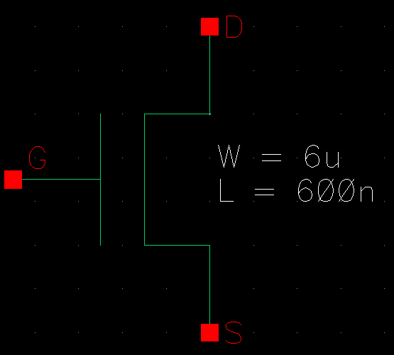
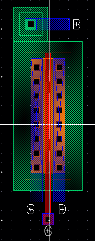
| NMOS/PMOS Layout | NMOS/PMOS Extraction | NMOS/PMOS Symbol | NMOS/PMOS Schematic |
 |  |  |  |
 |  |  |  |
Simulation for NMOS
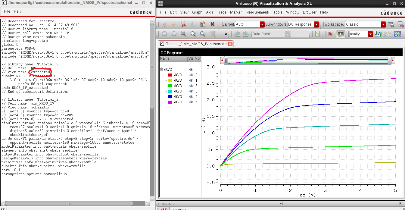
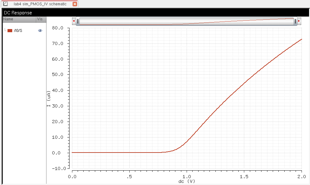
Simulation for PMOS
Lab:
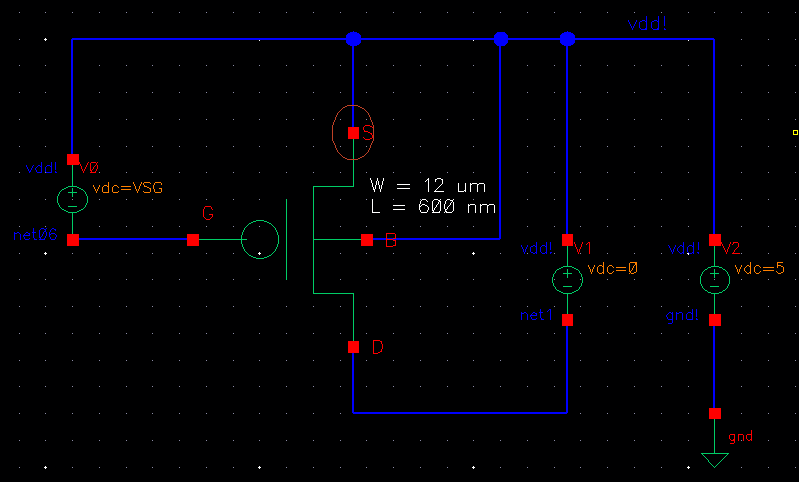
- Generate 4 schematics and simulations (see the examples in the Ch6_IC61 library, but note that for the PMOS body should be at vdd! instead of gnd!):
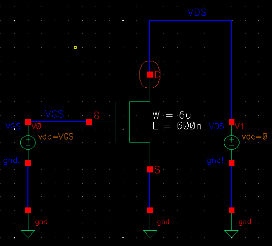
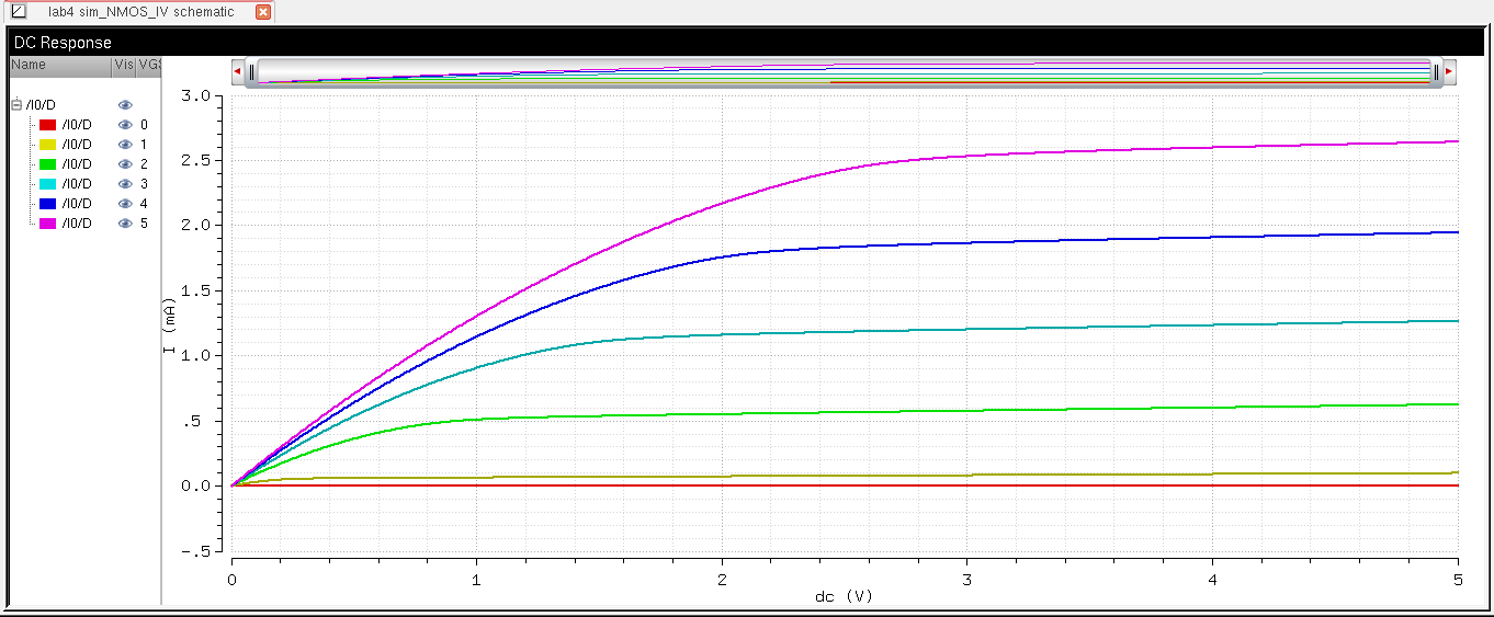
- A schematic for simulating ID
v. VDS of an NMOS device for VGS varying from 0 to 5 V in 1 V steps
while VDS varies from 0 to 5 V in 1 mV steps. Use a 6u/600n
width-to-length ratio.
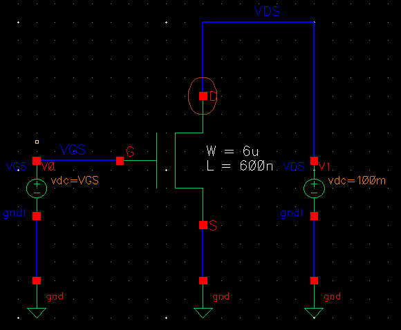
- A
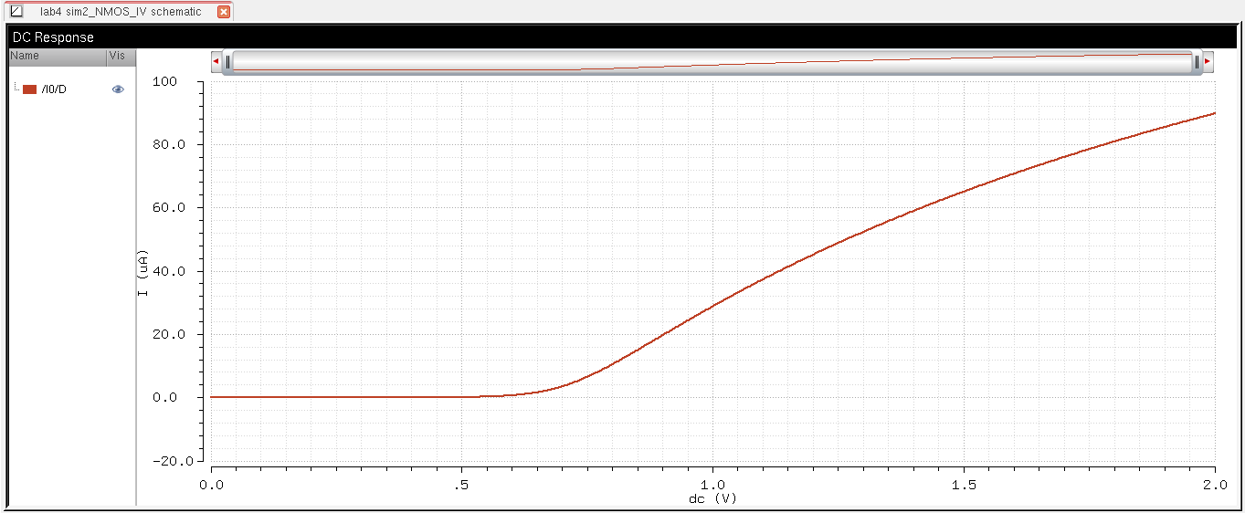
schematic for simulating ID v. VGS of an NMOS device for VDS = 100 mV
where VGS varies from 0 to 2 V in 1 mV steps. Again use a 6u/600n
width-to-length ratio.
- A
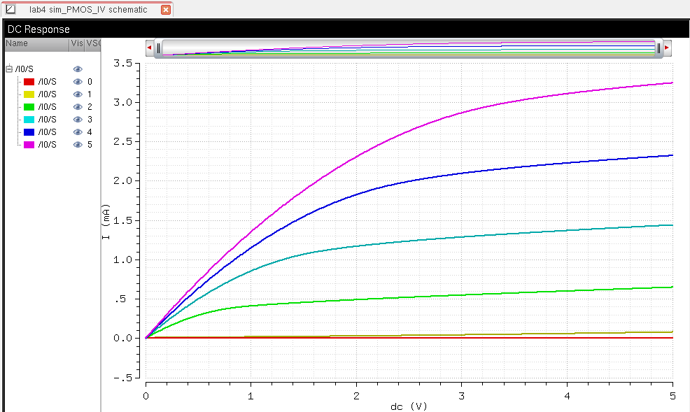
schematic for simulating ID v. VSD (note VSD not VDS) of a PMOS device
for VSG (not VGS) varying from 0 to 5 V in 1 V steps while VSD varies
from 0 to 5 V in 1 mV steps. Use a 12u/600n width-to-length ratio.
- A
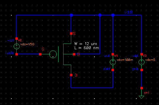
schematic for simulating ID v. VSG of a PMOS device for VSD = 100 mV
where VSG varies from 0 to 2 V in 1 mV steps. Again, use a 12u/600n
width-to-length ratio.
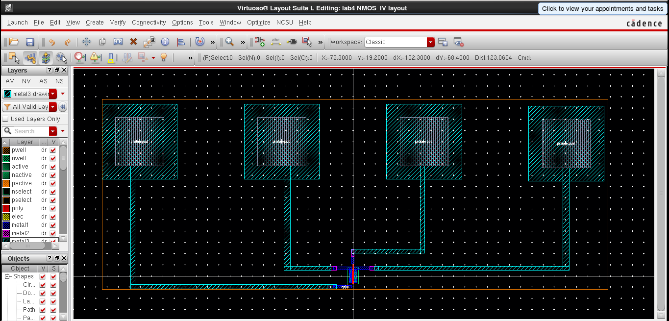
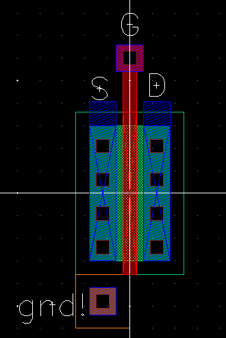
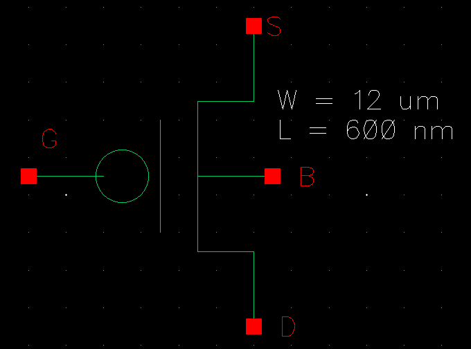
- Lay
out a 6u/0.6u NMOS device and connect all 4 MOSFET terminals to probe
pads (which can be considerably smaller than bond pads [see MOSIS design rules] and directly adjacent to the MOSFET (so the layout is relative small).
- Show your layout passes DRCs.
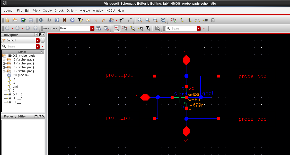
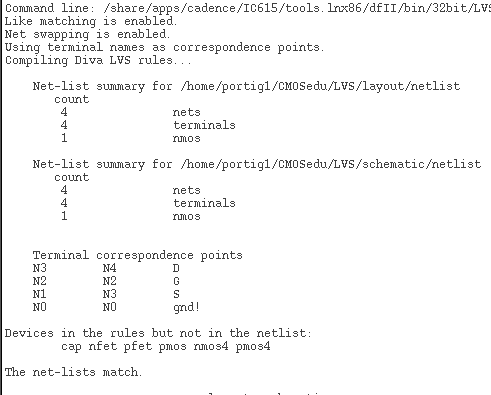
- Make a corresponding schematic so you can LVS your layout.
In the prelab, the NMOS was made
to these specficications so we can just reuse it and connect the
terminals to the probe pads.
Click on image to view layout without DRC box 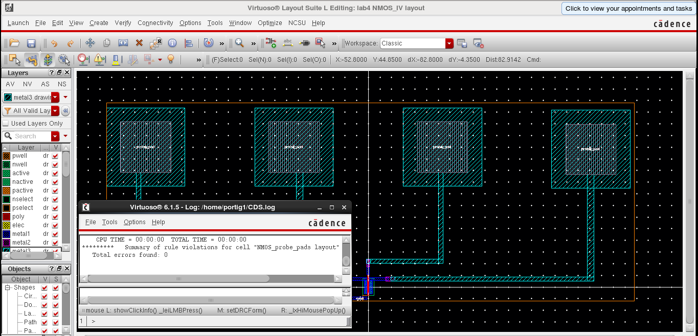
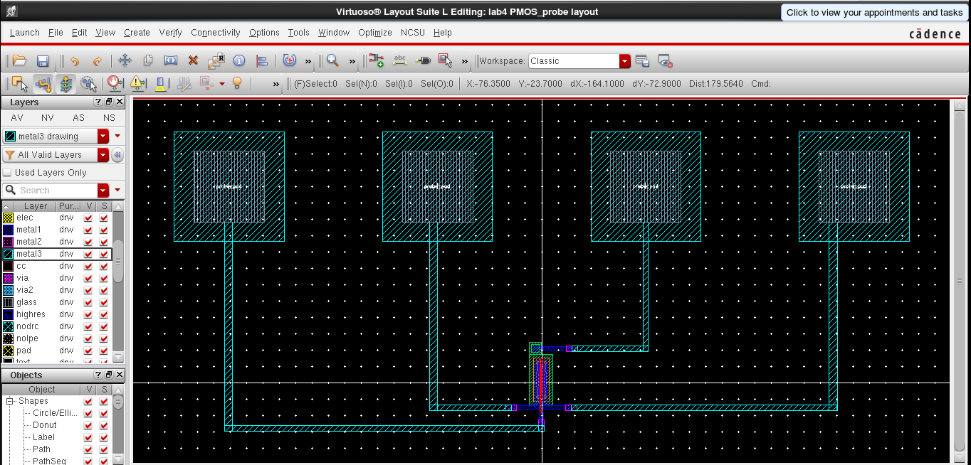
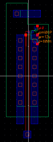
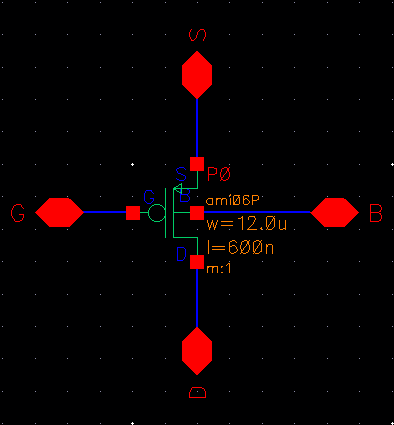
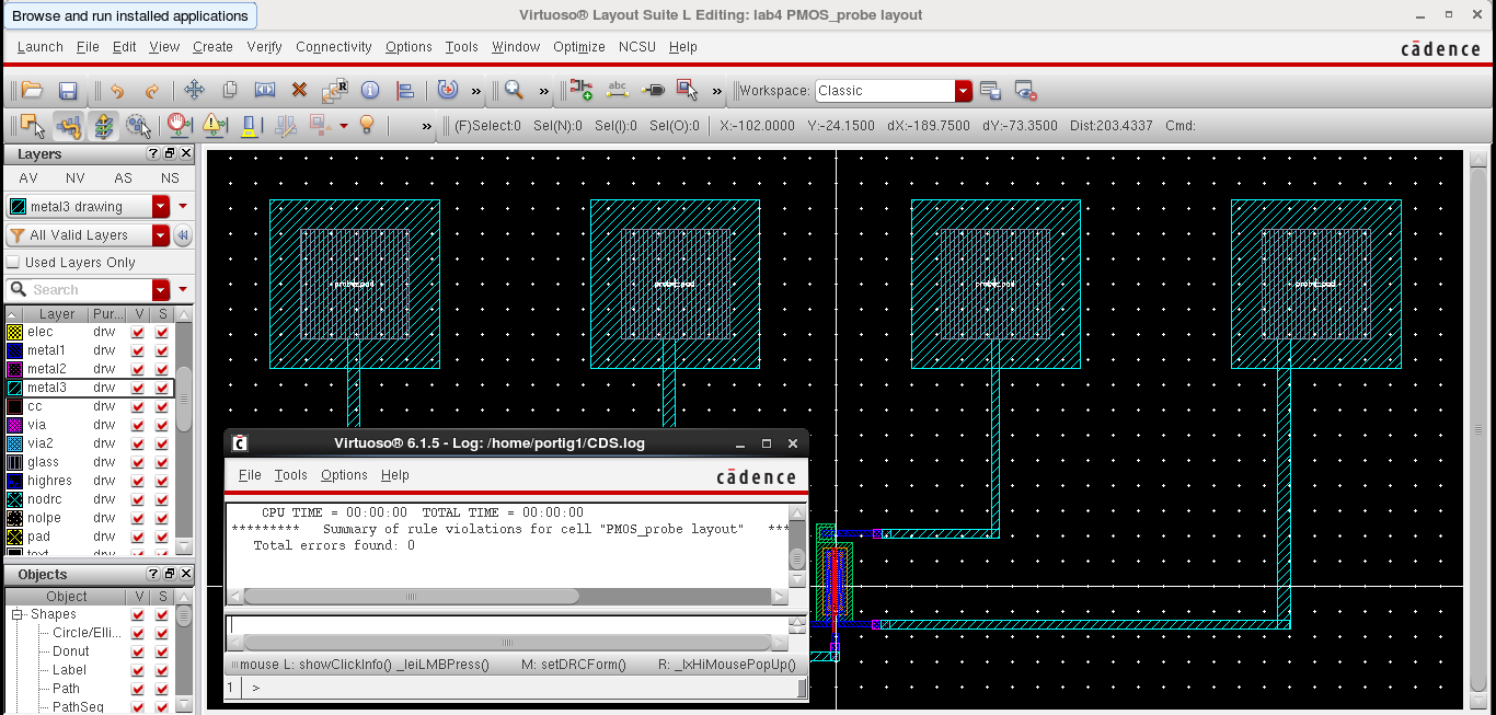
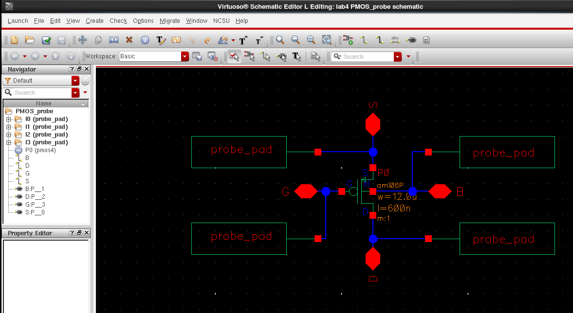
- Lay out a 12u/0.6u PMOS device and connect all 4 MOSFET terminals to probe pads.
- Show your layout passes DRCs.
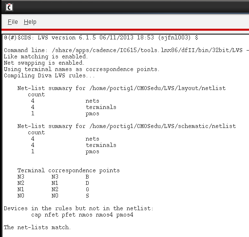
- Make a corresponding schematic so you can LVS your layout.
As with the NMOS, the PMOS was also laid out in the prelab.
Click on image to view layout without DRC box
Ensure that your html lab report includes your name and email address at the beginning of the report (the top of the webpage).
When finished backup your work (webpages and design directory).
Return to EE 421 Labs