Lab 3 - ECE 421L
Authored
by Geovanni Portillo,
September 11, 2019
Email: portig1@unlv.nevada.edu
All images can be clicked on to view larger versions
Lab Description: This lab will focus on the layout of the 10-bit DAC you designed and simulated in Lab 2
lab3.zip available here
Prelab:
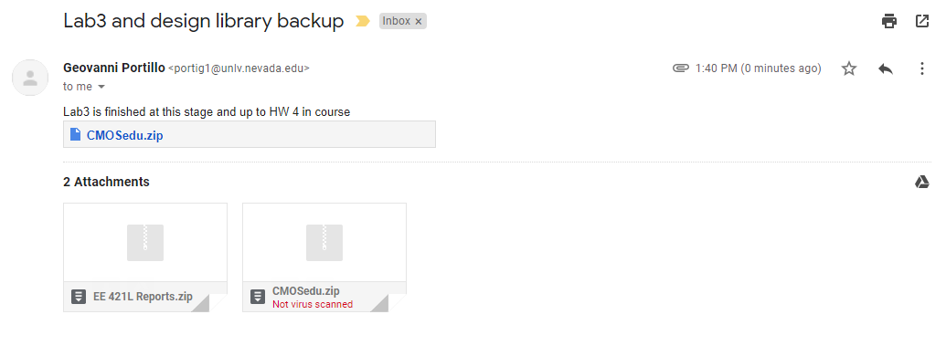
Previous work from labs and courses has been backed up via email
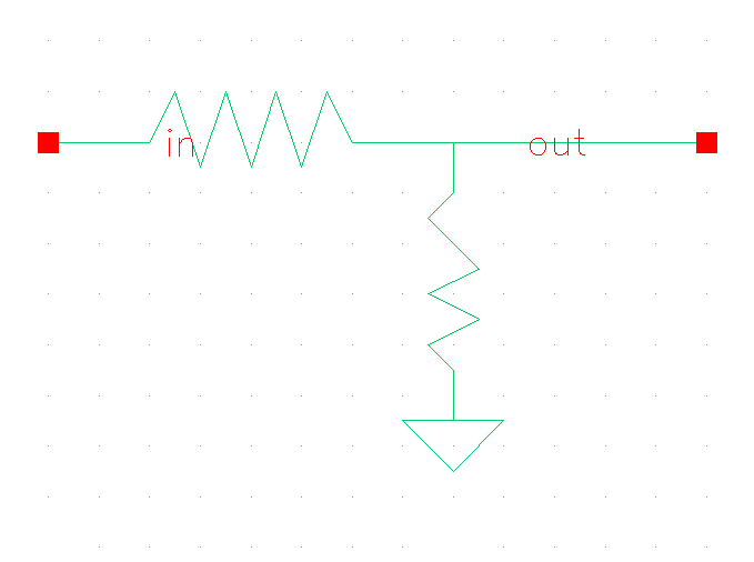
Finishing Tutorial 1 from the pre-lab of lab 1, the next step is to create a symbol for the voltage divider and then use it in a seperate cellview for simulation.
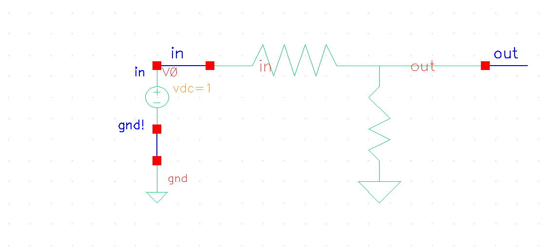
The
next step was to then layout the 10K resistor and verify it by a design
rule check (DRC) and extraction to confirm the resistivity.
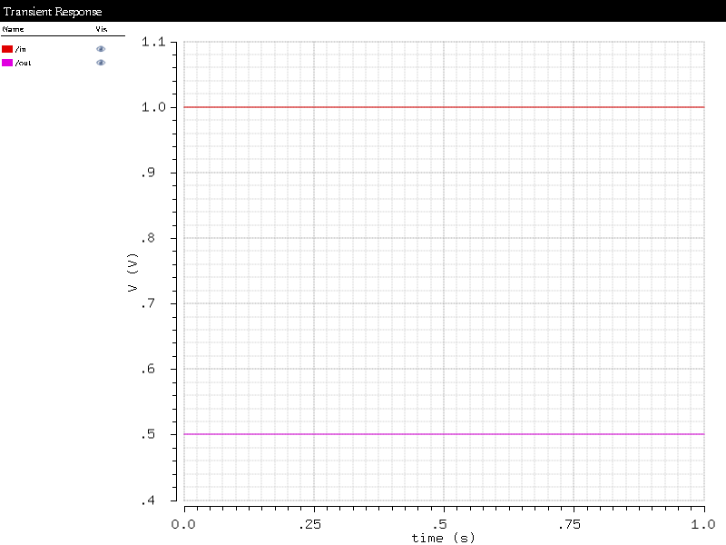
After
that, we create a layout of the divider and complete the same
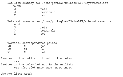
verification steps with the addition of doing a layout versus schematic
(LVS) to check if the netlists match.
Lab:
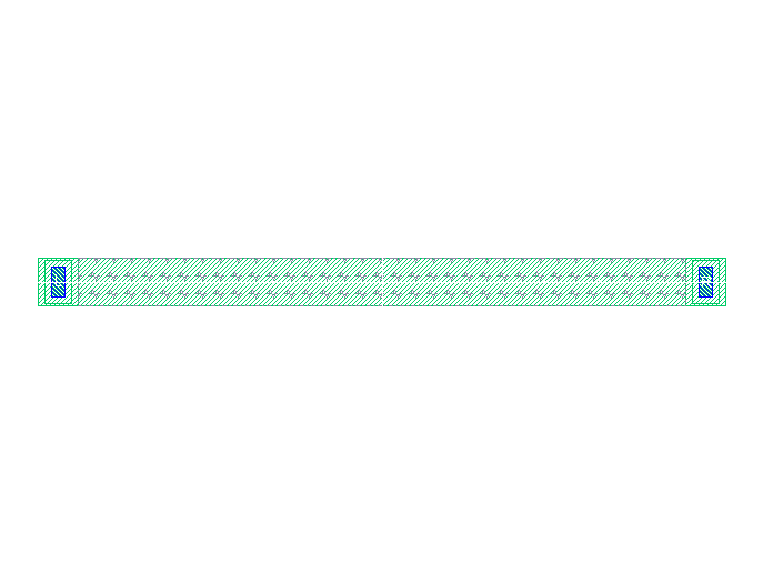
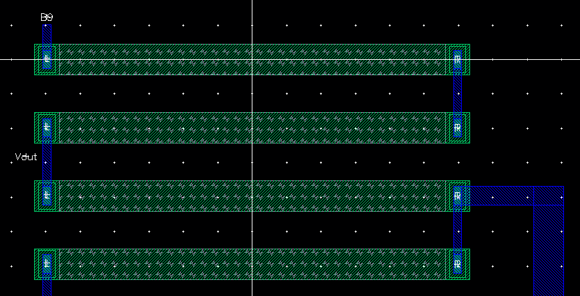
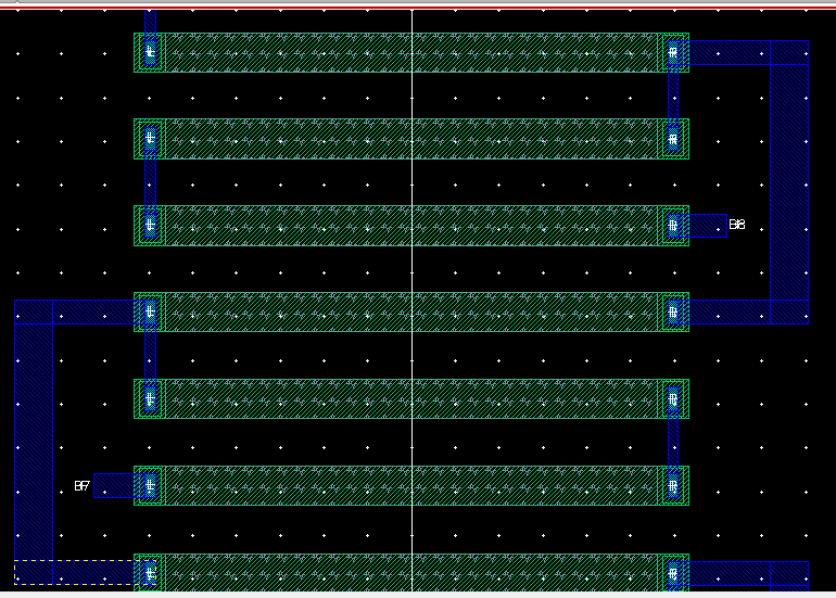
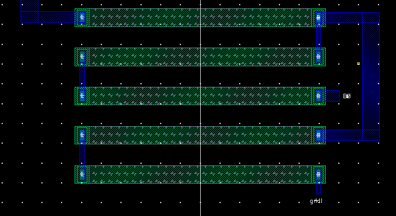
- Use the n-well to layout a 10k resistor as discussed in Tutorial 1
- For the n-well, I copied the R_N_well_10K cell that was completed for Tutorial 1 using the instructions found here.
- To select the width and length of the resistor, the following formula R= Rsquare*(L/W) can be used. With width given as 4.5um from the tutorial, the length can be solved with L = R*W/Rsquare. Rsquare is also given as roughly 800um/square and we want a 10K resistor so R = 10K. Then L = 10K * 4.5/(800/square) = 56.25um..
In the tutorial, a length was picked as 56um but that did not pass the
DRC as the length, and the width, has to be divisible by 0.15um.Instead, length was changed to 56.1um and that did pass.
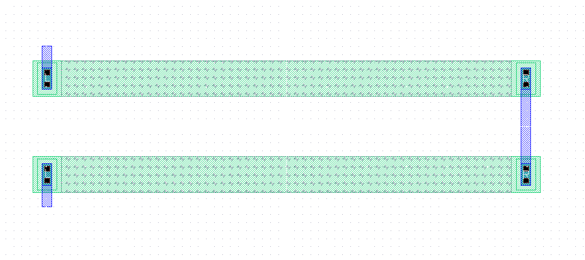
- Use the n-well in your layout of the DAC
- Note:
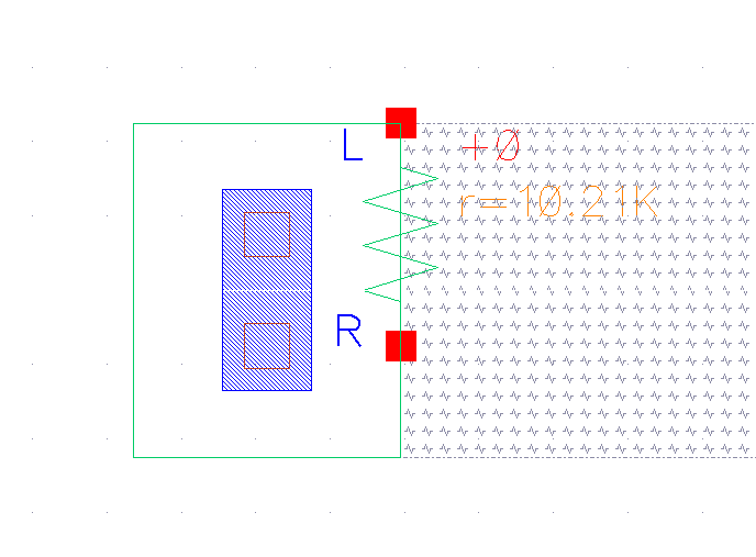
when centered on the origin, the bottom of the n-well resistor extends
2.25um up and down the y-axis. This is important to remember as each
resistor needs to be at minimum 5.4um away from one another on the
y-axis. So in layout view, if you edit a resistor by using q, you can
change its x and y values. Using that, each resistor can be set away
the appropriate distance from each other by moving in increments of
9.9um. 5.4um from each other, then 2.25um from each of the centers.
- Additionally, all resistors are centered at x = 0 with varying y positions. Also, all pins and connections are on metal1.
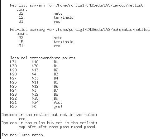
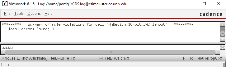
- DRC and LVS, with the extracted layout, your design (show the results in your lab report)
- Zip up your final design directory and place it in
the lab3 directory, with a link on your lab report, so the grader can
examine both the layout and schematic (and simulations)
- lab3.zip located here and at the top of the page
- The
lab as well as the design libraries have been backed up. This contains
everything up to 9/11/2019 done both in lab and course.
Return to EE 421 Labs