Lab 2 - ECE 421L
Prelab:
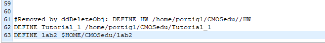
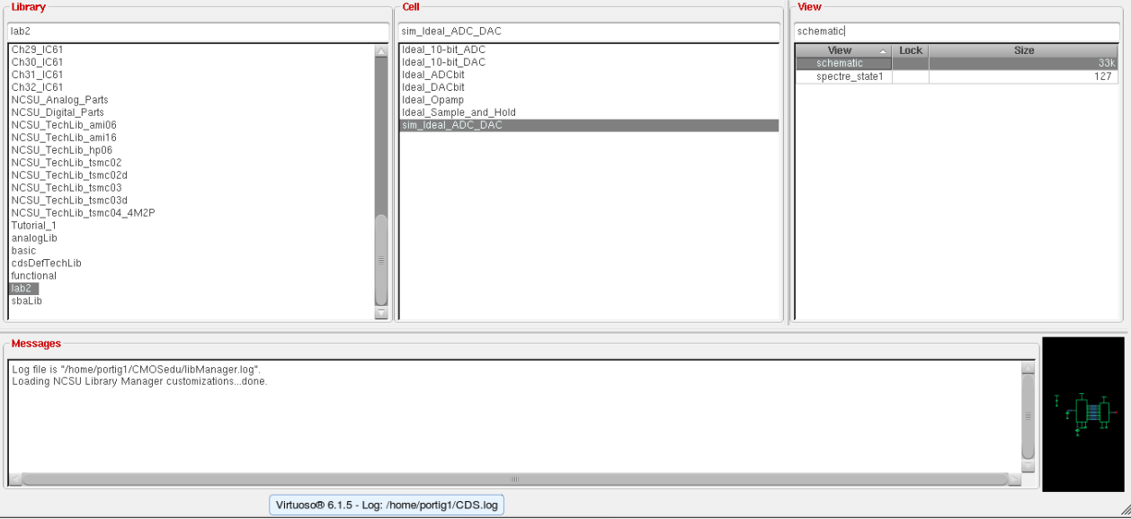
We need to add the lab2 library to our design directory and update the cds.lib file to be able to use it
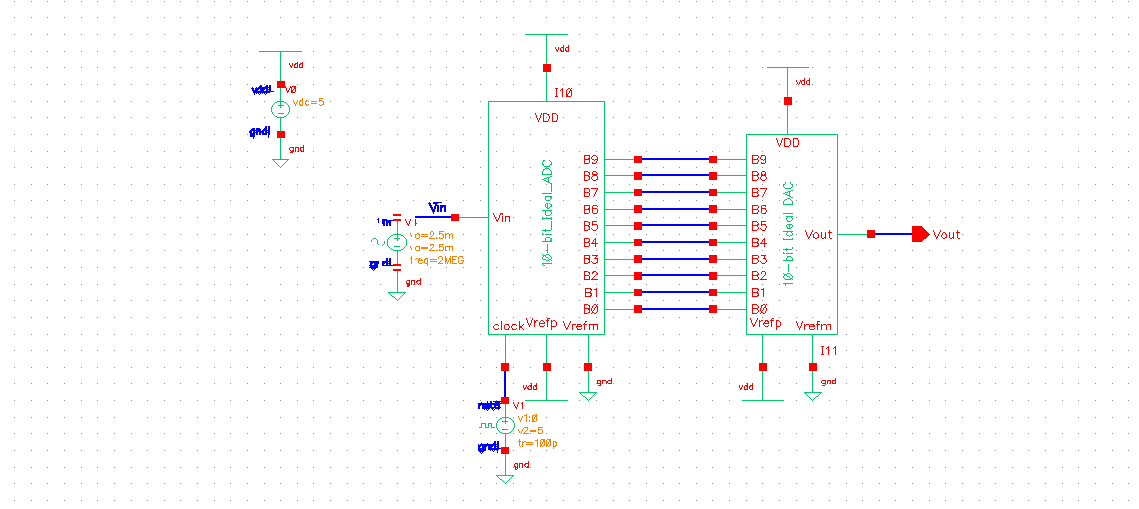
I changed amplitude and offset of Vin to 25mV to get the following plot. Line width, style, and color were changed to demonstrate understanding of how to change aesthetics.
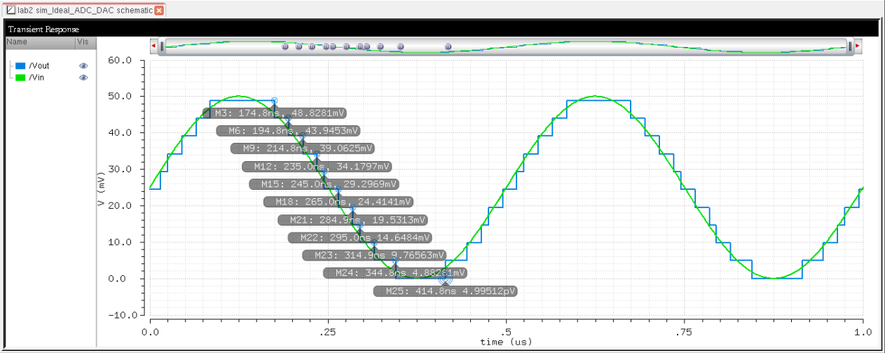
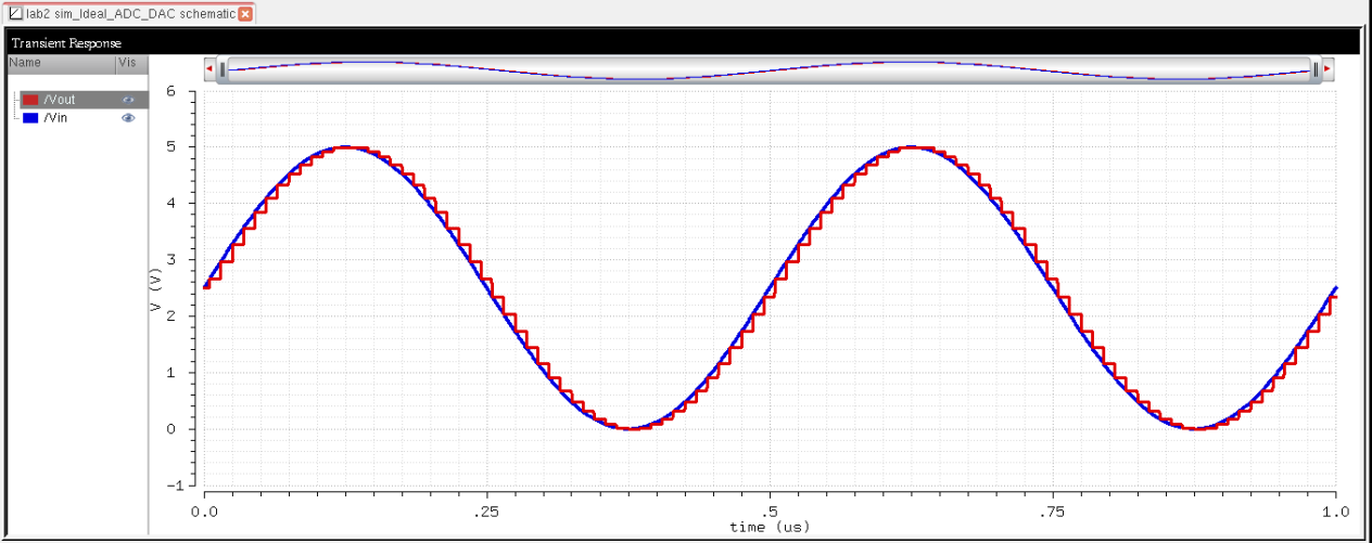
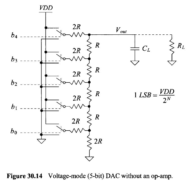
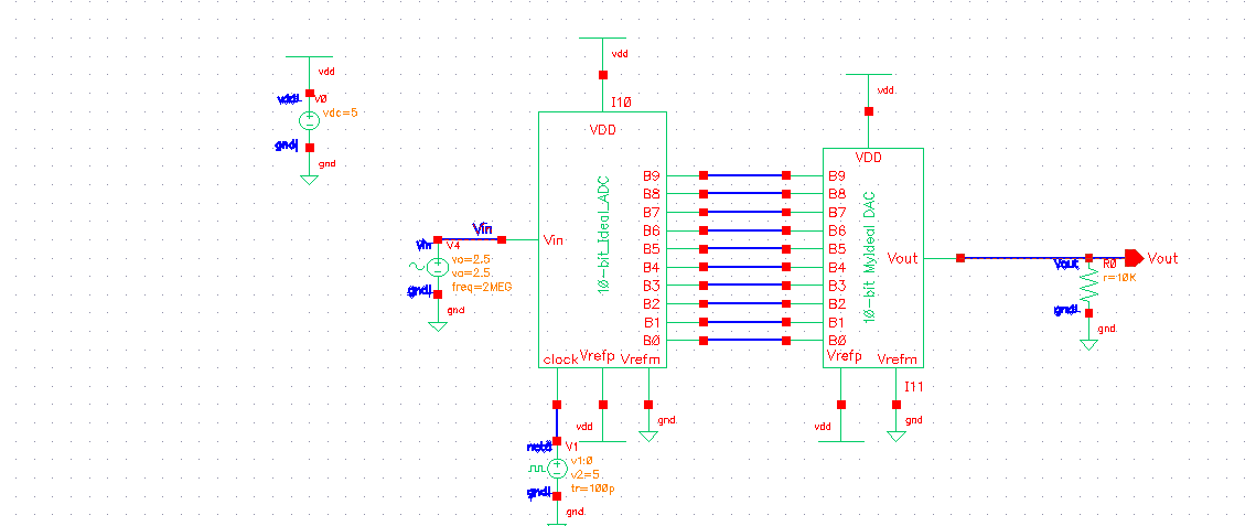
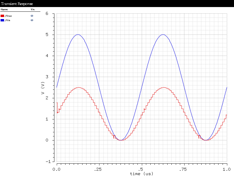
In the circuits above, we have an ADC taking our Vin then converting that in a 10-bit value across B[9:0] to the DAC which then converts our value back out in a analog signal. From Figure 30.14 below, we can determine the LSB for both plots since VDD was kept the same.
LSB = 5V/2^10 ~= 4.88mV
So each step or bit is gonna represent 4.88mV. That is why in the second plot, we have 10 steps since our amplitude is 25mV.
Lab:
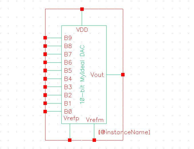
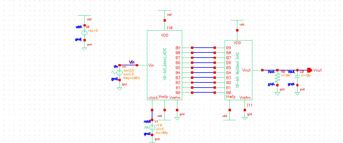
First I made a schematic for the 10-bit DAC using an n-well R of 10K then created the symbol view with the exact same footprint as the Ideal_10-bit_DAC .
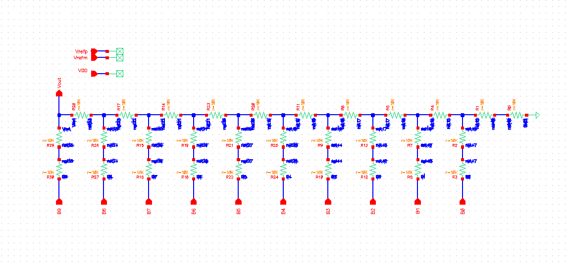
To get the total output resistance, the formula to get the equivalent parallel resistance [Rt = R1*R2/(R1+R2)] and for series resistance (Rt = R1 + R2) are used. And doing so from the right to left side, we can find that the output resistance equals R (10K in the context of this lab).
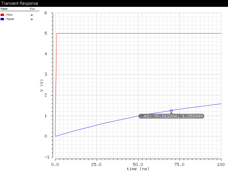
In the following circuit, all inputs are grounded except B9 which has a pulse source going from 0 to VDD (5V). I verify that the result from using 0.7RC to calculate the delay for a 10pF load matches the simulation results.
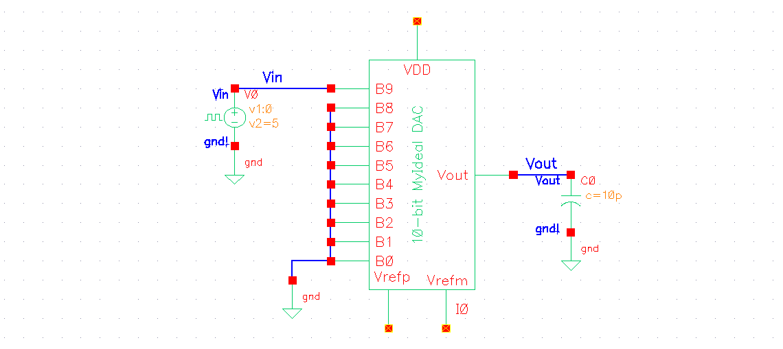
The calculation 0.7RC = 0.7(10K)(10pF) = 70ns matches with the expected result of about 1.25V at 70ns
To further verify that the design is working similarly to Ideal 10-bit DAC, I copied the simulation cell from the prelab and replaced the Ideal DAC with mine and ran the simulation again.

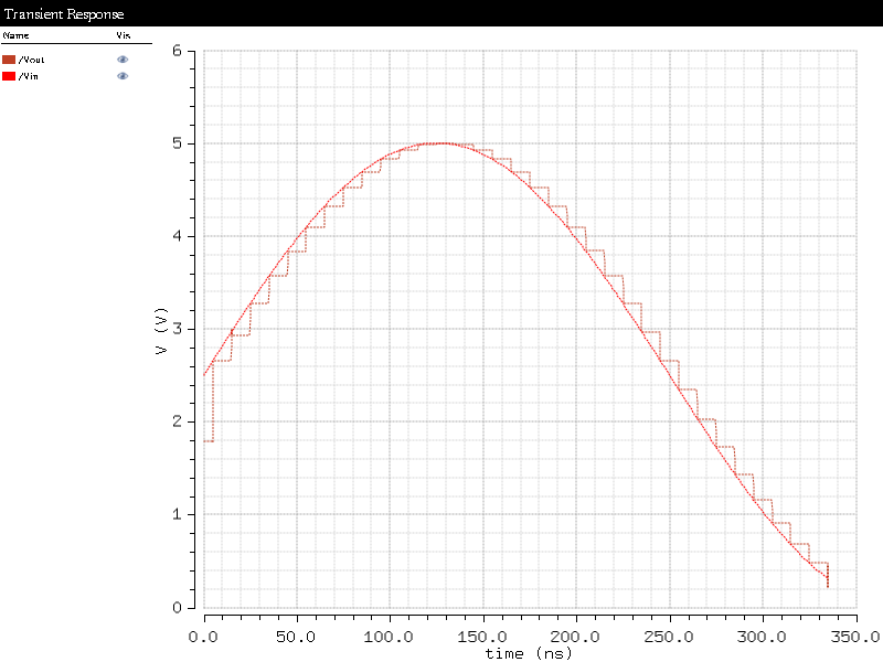
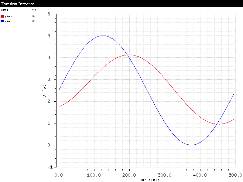
There was an issue with the simulation not converging as the plot shown is different from the Ideal
from the prelab. To fix this, the simulation needs to be forced to
converge by going to, in the ADE, Simulation -> Options -> Analog
and then setting the following values. The downside being the accuracy
of the simulation will be degraded.
Relative tolerance, reltol, of 10% (= 1e-1)
Voltage absolute tolerance, vabstol, of 100 mV (= 1e-1)
Current absolute tolerance, iabstol, of 1 mA (= 1e-3)
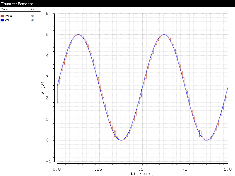
The following plot is the result from changing these settings.
Below are schematics and simulations for driving R/C/RC loads
R load of 10K
C load of 10pF

RC load of 10K and 10pF
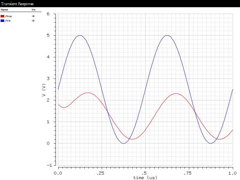
When we drive a 10K resistor as the load, we see it functions as a voltage divider. Being that it and the total output resistance are equal, are output voltage is halved as seen in the plot.
If the resistance of the switches (Fig 30.14) are not small compared to R, then the overall output voltage will decrease. As you go up from ground and find the equivalent resistances at each intersection, the equivalent resistance increases somewhat. If the resistance of a switch was for example 0.5R, then the first equivalent resistance would be 1.11R repeating, the second would be 1.145R, the third 1.154R, the fourth 1.157R, the fifth 1.158R, and the sixth through eigth as 1.158R again. This would result in the top branch for bit 9 having a resistance of 2.5R and the bottom branch having a resistance of 2.158R. Since the circuit would act as a voltage divider, the output would when Vin is 5V would be equal to 5V * 2.158R/(2.5R + 2.158R) = 2.32V. This is lower compared to if the resistance in the switch was minimal and Vout would be equal to 5V * 2R/(2R + 2R).
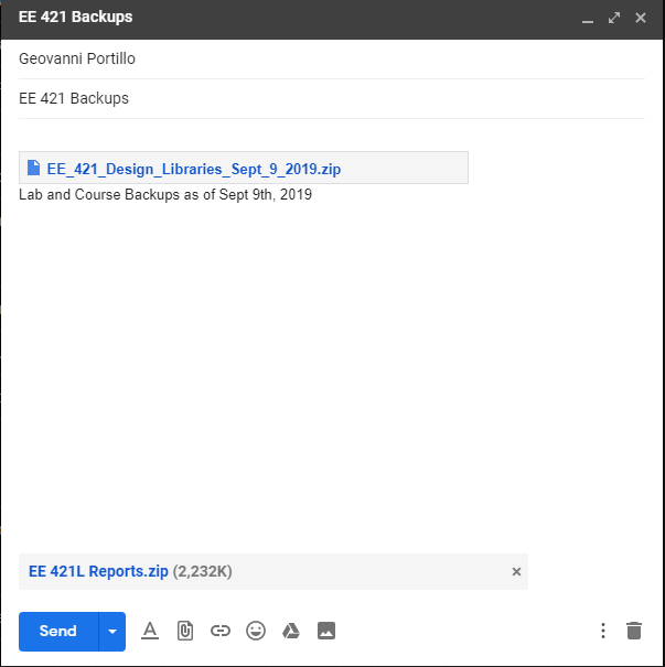
Labs and course files have been backed up