Lab 06 - EE 421L
Authored
by Cody Jones,
E-mail:
Jonesc30@unlv.nevada.edu
10/19/18
Lab 06: Design, layout, and simulation of a CMOS NAND gate, XOR
gate, and Full-Adder.
----------------------------------------------------------------------------------------------------
Prelab:
To
view the pictures larger, right click on image and open in new tab.
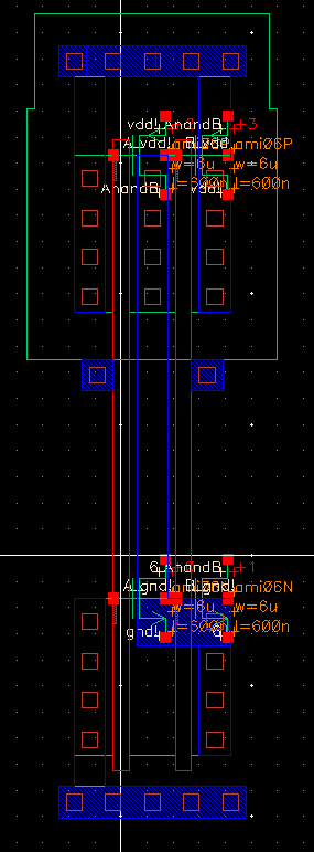
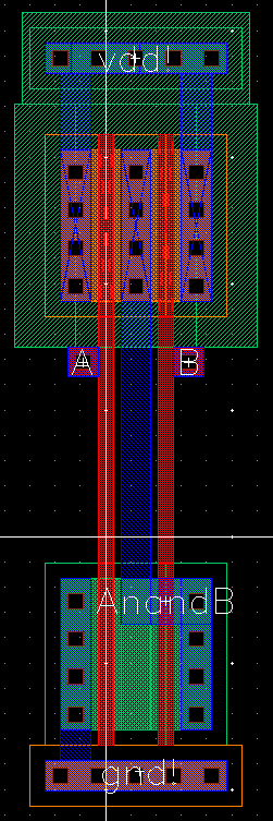
Go
through tutorial 4. This was creating an NAND gate. Since we have to create our
own NAND gate with our initials in the lab, I will post the schematic, layout
and extracted below for the lab content since they are the same.
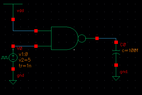
|
Simulation
for the prelab NAND gate |
|
|
|
|

----------------------------------------------------------------------------------------------------
Lab:
Step 1: Draft the schematics of a 2-input NAND gate (Fig. 12.1), and a 2-input XOR gate (Fig. 12.18) using 6u/0.6u MOSFETs (both NMOS and PMOS).
Create
layout and symbol views for these gates showing that the cells DRC and LVS
without errors.
|
NAND
Schematic |
NAND
Symbol |
|
|
|
|
NAND
Extracted |
NAND
Layout |
|
|
|


The
DRC and LVS (with FET parameters on) approved
![]()

|
XOR
Schematic |
XOR
Symbol |
|
|
|
|
XOR
Layout |
XOR
Extracted |
|
|
|


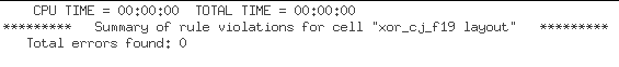
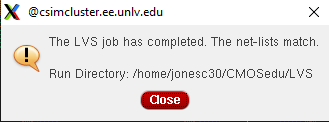
The
DRC and LVS (with FET parameters on) approved
Step 2: Simulation of the NAND and XOR.
|
Schematic
for simulation |
Graph
of the inputs and outputs |
|
|
|
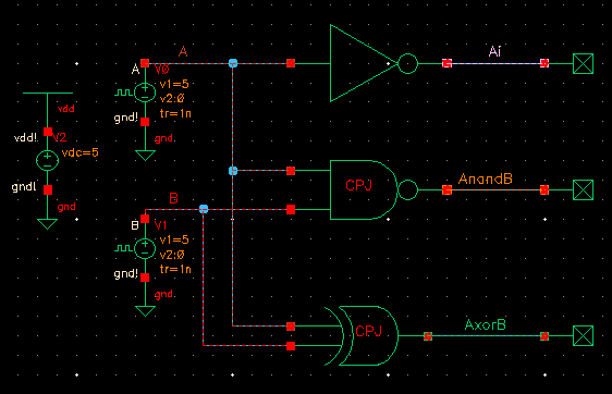

Glitches are caused by the input voltage not fully being 0V and 5V. For example, on my simulation at 200ns, A is switching from 0V to 5V and B is also switching at that time from 5V to 0V. Since, it takes a nanosecond to make the transition, the output AxorB will try to go to zero because both A and B are not high for that nanosecond. The input has to be 5V to get a digital 1 for the gates.
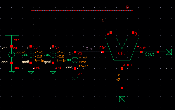
Step 3: Using these gates, draft the schematic of the full adder. Create a symbol for this full-adder.
Simulate,
using Spectre, the operation of the
full-adder using this symbol. DRC and LVS your full adder design.
|
Full-adder Schematic |
Full-adder Symbol |
|
|
|
|
Full-adder Layout |
Full-adder Extracted |
|
|
|


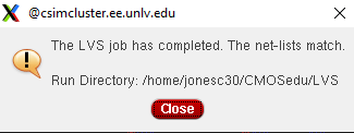
The
DRC and LVS (with FET parameters on) approved
![]()
Step 4: Simulation for the full-adder.
|
Schematic
for simulation |
Simulation
with the inputs and outputs |
|
|
|

----------------------------------------------------------------------------------------------------
This
Concludes the Lab 6 Report.