Lab 03 - EE 421L
Authored
by Cody Jones,
E-mail:
Jonesc30@unlv.nevada.edu
9/23/18
Lab 03: Layout of NMOS and PMOS devices in ON’s C5 process.
----------------------------------------------------------------------------------------------------
Prelab:
|
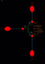
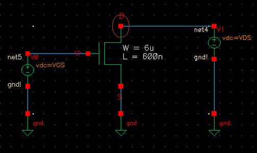
NMOS schematic |
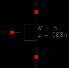
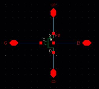
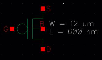
NMOS symbol |
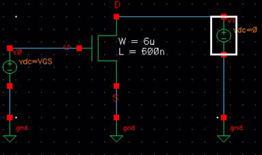
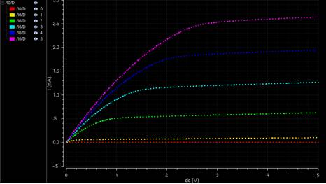
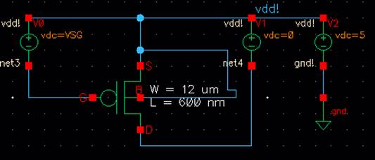
Sim of NMOS circuit |
|
|
|
|
|
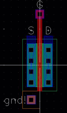
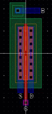
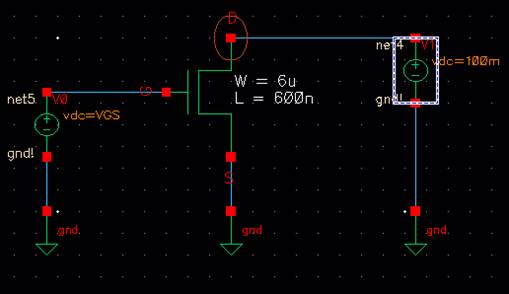
Layout of NMOS |
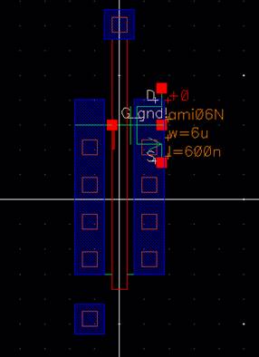
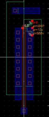
Extracted layout |
Simulation |
|
|
|
|
|
PMOS schematic |
PMOS symbol |
Sim of PMOS circuit |
|
|
|
|
|
Layout of PMOS |
Extracted layout |
Simulation |
|
|
|
|
----------------------------------------------------------------------------------------------------
Lab:
Step
1:
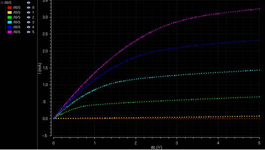
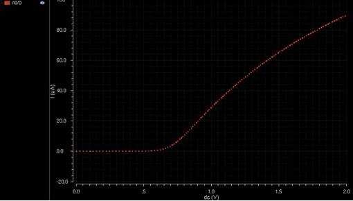
Sim the NMOS Id v VGS
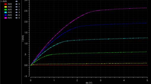
Sim
the NMOS Id v VDS
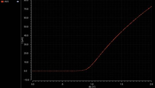
Sim
the PMOS Id v VSD


Sim
the PMOS Id v VSG

Step 2:
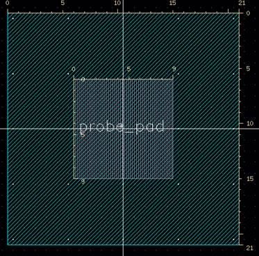
For
the probe pads
|
|
|
|


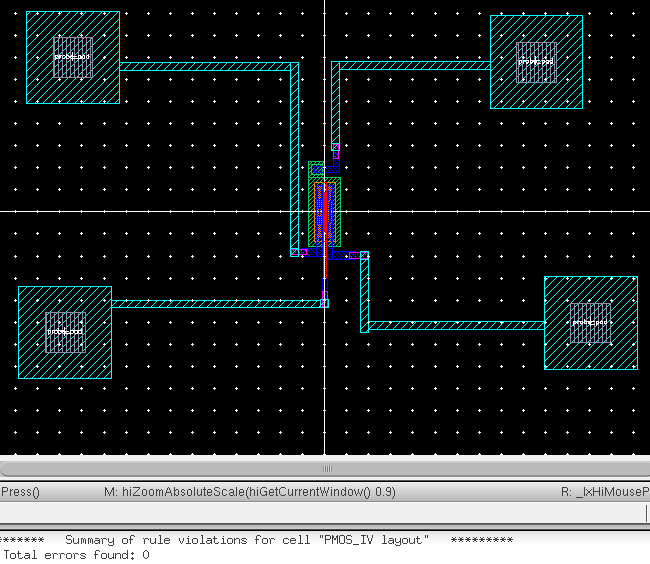
Layout
of the NMOS 6u/0.6u with proof of DRC
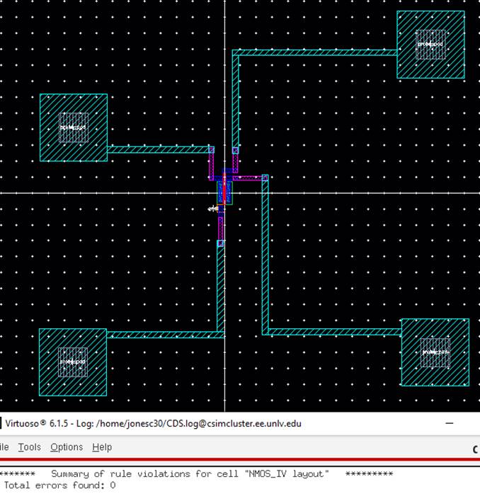
Schematic
representing NMOS with probe pads
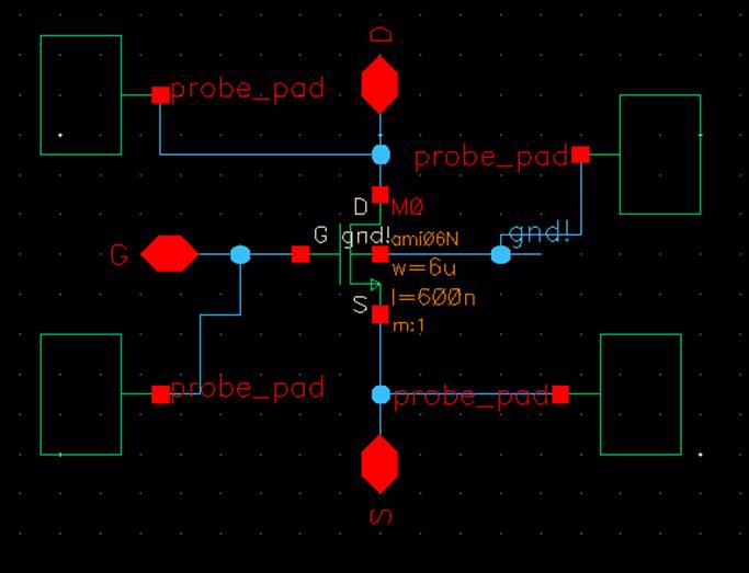
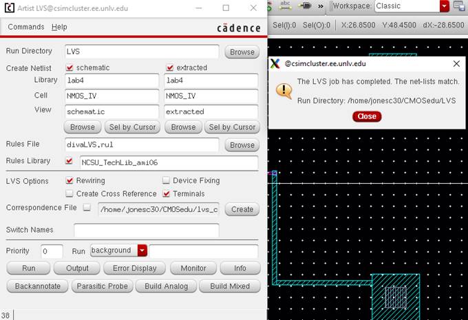
My
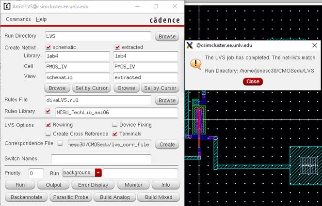
design satisfies LVS
Step 3:
Layout of PMOS with probe pads and DRC verification
Schematic of PMOS with probe pad connections
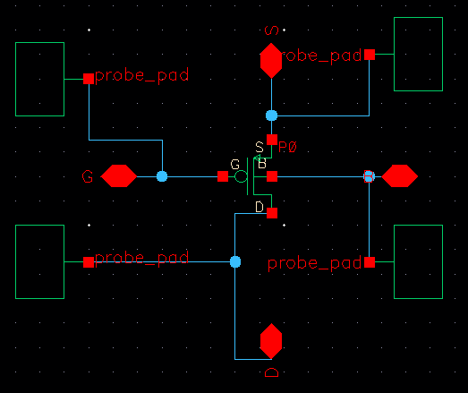
My design satisfies LVS