Lab 3 - ECE 421L
PRELAB
Finish Tutorial 1
(In Tut.1 we
created the layout of a resistive voltage divider)
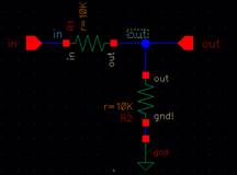
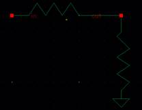
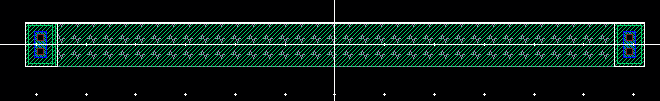
We created a
Schematic (Fig1), Symbol(Fig2), a layout (Fig3),
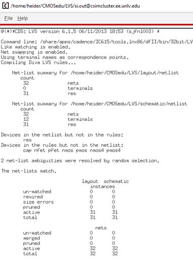
and did a LVS check (Layout VS Schematic)
LAB3
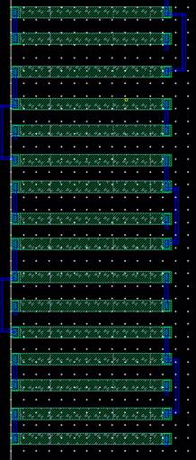
In LAB 3 we
are using the n-well to layout a 10k resistor
(Tutorial 1)
We will use
this n-well resistor in the layout of our DAC, then we will verify with LVS
that they match.
ð How to select
the width and length of the resistor (according to MOSIS):
L = 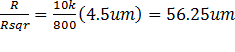
Thus, L = 56.25um and W
= 4.5um
Although, Cadence didn’t agree with
56.25 since it is not divisible by .15 – thus changed 56.25 to 56.1.
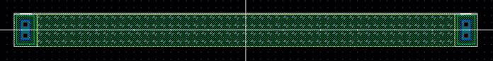
1)
Just
as in Tutorial 1 – we created a 10k resistor:
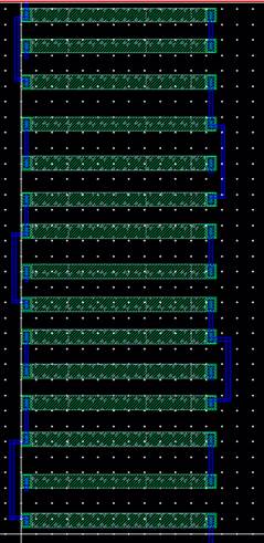
2) To measure the width and
length of the resistor you can use the
ruler (bindkey- k) or you can hit “q” to view the
properties of the
dimensions of your resistor.
-
The
x positions are all the same as I lined them all up with the
y-axis marking line, as well as checked with a ruler.
4) DRC Check
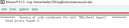
5) LVS Check (Layout VS
Schematic)
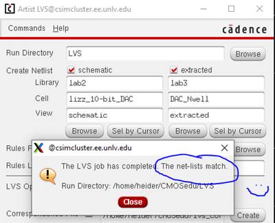
noting that ‘lizz_10-bit_dac’ is
the schematic of my
10-bit DAC.