EE 421L – Digital IC Design Lab – Project
Clock Signal Multiplier
Author: Darryl Derico
E-Mail:
derico@unlv.nevada.edu
11/13/2019
Zip File: lab_project.zip
Project Description:
The goal of this project is
to design a circuit that would take a 9 to 11 MHz clock signal and increase it
to a 36 to 44 Mhz. clock signal.
(Part 1) Schematics used:
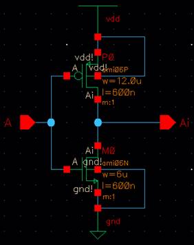
Inverter (12u/.6u):
This inverter is used as my
standard inverter of “short length.”
The measurements on the
symbol represent the width and length of the PMOS respectively. The width of
the NMOS is half of the width of the PMOS, while the length NMOS and PMOS are
equal. Since it is of short length, it should not contribute any significant
amount of delay to the overall circuit.

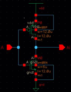
Inverter (12u/12u):
The 12u/12u inverter is used
as the “long-length” inverter. Its main purpose is to generate a significant
delay between its input and output.
Putting these in series will
increase the delay in the circuit it is implemented in. The measurements of the
PMOS and NMOS can be obtained through the symbol in the same way as the short
length inverter.

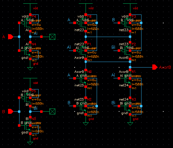
XOR Gate:
The XOR gate will be
responsible for the comparison between the original clock signal and the clock
signal after it is delayed by a quarter of its period. If done correctly, the
output of the XOR gate would be a signal that is twice as fast as the original
clock signal.
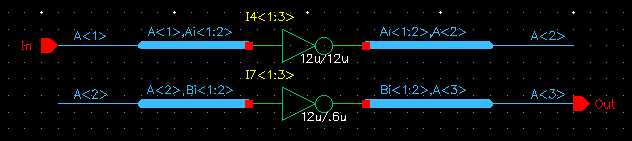
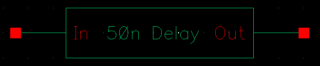
50ns Buffer:
This buffer consists of 3
long length inverters and 3 short length inverters. The 3 long length inverters
will contribute to the delay while the 3 short length inverters will square out
the resulting wave. In order to keep the signal equivalent to the original
signal but with delay, an even number of total inverters must be used which is
why 3 short length inverters are used instead of the minimum 2 to square out
the wave. Only the original clock signal will run through this, and its output
will go through the first XOR gate to be compared with the unaltered clock
signal.
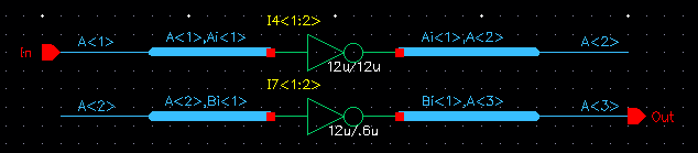
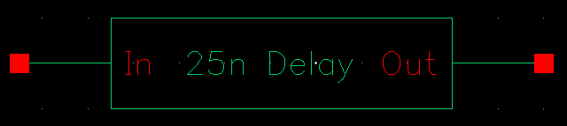
25ns Buffer:
The 25ns Buffer acts just
like the 50ns, but only delays the input signal by 25ns instead of 50. It uses
2 long length inverters, and 2 short length inverters. Its purpose in the
schematic is to create a delayed signal on the output of the first XOR gate.
Its output would go into the second XOR gate to be compared with the unaltered
output of the first XOR gate.
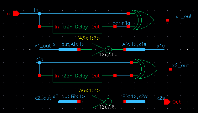
4X Clock Multiplier
(Simulation and Schematic):
The 4x clock multiplier
utilizes two edge detectors in series. The input “in” is representative of the
original clock signal and is connected to the 50ns buffer. The original clock
signal and the buffer output would then be run through an XOR gate. This
creates the first edge detector and makes a signal that is twice as fast as the
original clock signal. From there, the signal is run through two short length
inverters to square out the waveform. Finally, it is plugged into another edge
detector with a 25ns buffer instead of a 50ns buffer. Once output through the
second XOR gate, the signal is equivalent to 4 times the frequency of the
original clock and squared out again to make the final output of the entire
multiplier.
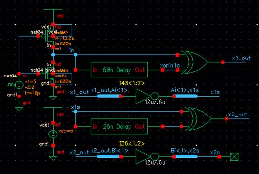
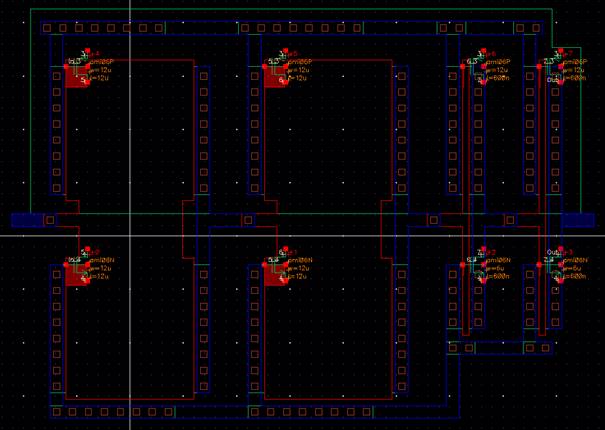
Schematic:
Simulations:
To simulate the clock signal,
a pulse signal was connected to a transistor-level inverter which would output
an input signal that would run through the signal multiplier. This was done so
that all traced signals, including the input, would not exceed vdd.
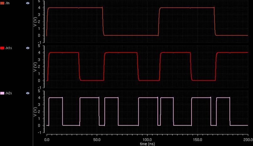
4V @ 9MHz frequency:
5V @ 10MHz frequency:
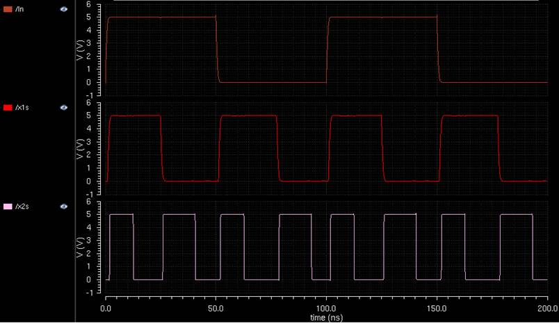
6V @ 11MHz:
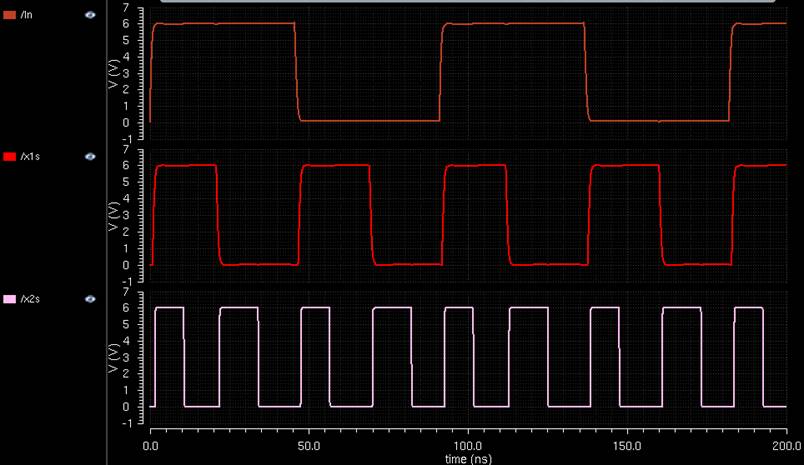
From the simulations, it is
noted that lower voltages require lower frequencies and vice versa for the output
wave to still be visibly acceptable. When a voltage or frequency is not
adjusted accordingly, the waves start to overlap and create a noticeably
inconsistent duty cycle with varied widths, and hazards.
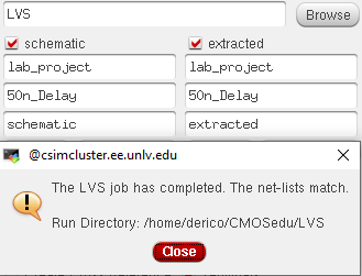
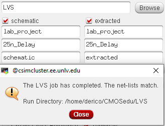
(Part 2) Layouts &
Verifications:
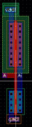
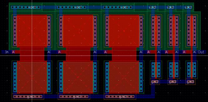
Inverter (12u/.6u):
This is the layout of the
standard inverter created in Tutorial 3.
![]()

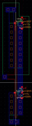
Inverter (12u/12u):
The 12u/12u inverter’s layout
is the same as the standard inverter, except the lengths and widths of both the
PMOS and NMOS are increased to both be 12u.
![]()

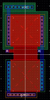
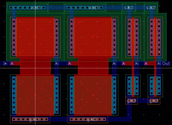
XOR Gate:
Responsible for the
comparison between an original signal and a delayed signal in this particular
project, this layout is used twice in the final schematic.
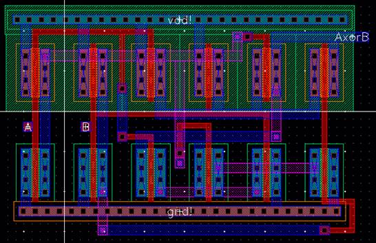
![]()

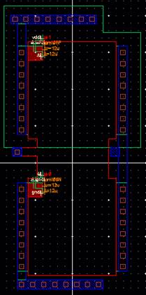
50ns Buffer:
This layout will take in the
original clock cycle and output a delayed equivalent of it. It consists of 3
long length inverters followed by 3 short length inverters.
![]()
25ns Buffer:
The last buffer in the
schematic, this layout will receive the output of the 1st XOR gate
and delay it to create another equivalent but delayed signal before sending it
the last XOR gate.
![]()
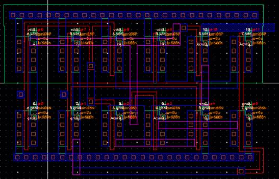
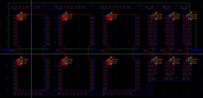
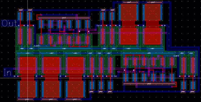
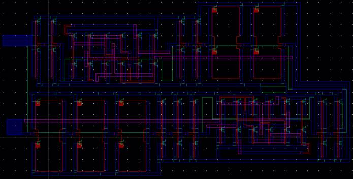
4X Clock Multiplier
(Layout):
The bottom half of the layout
from left to right, consists of the Input terminal indicated by large “In”
label, the 50 ns buffer, and the 1st XOR gate. The XOR gate is
followed by 2 short length inverters to help square out its output before
sending it to the next XOR gate and 25 ns buffer.
The top half of the layout from right to left, consists of the 25 ns buffer and
the 2nd XOR gate followed by another 2 short length inverters to
square out the output which result in the output terminal indicated by the
large “Out” label.
![]()