EE 421L – Digital IC Design Lab – Lab 7
Using buses and arrays in
the design of word inverters, muxes, and high-speed adders
Author: Darryl Derico
E-Mail: derico@unlv.nevada.edu
11/6/2019
Lab Description:
In this lab, we are to first
design, layout, and simulate a ring oscillator and learn how to implement buses
and arrays into the designs of word inverters, muxes, and high-speed adders.
Prelab:
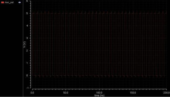
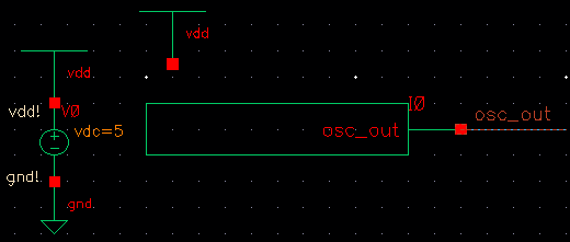
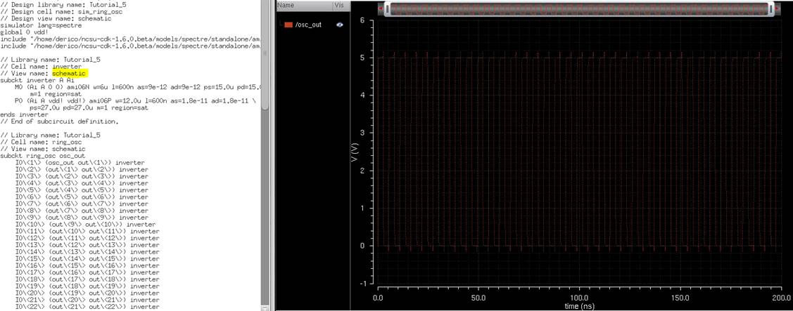
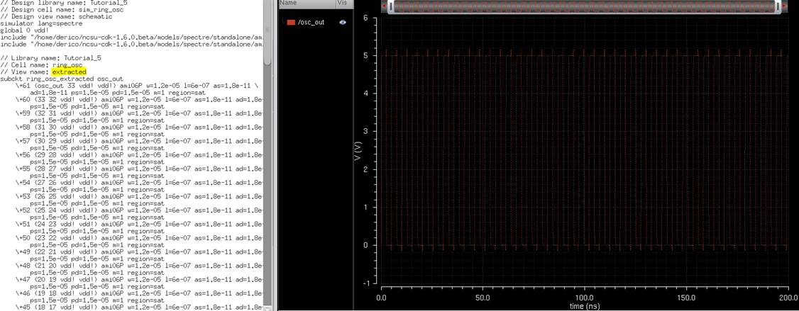
Went through Tutorial 5 to design,
layout, and simulate, a ring oscillator.



Lab:

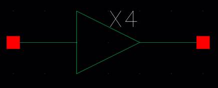
Created a cellview to
simulate the 4x inverter.
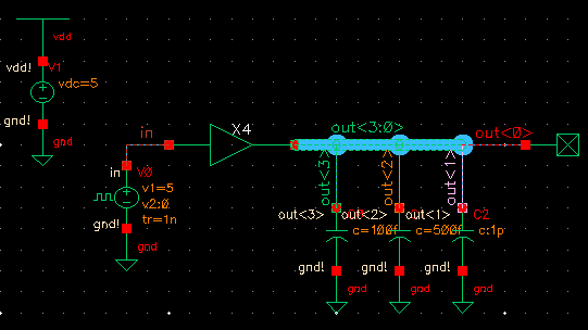
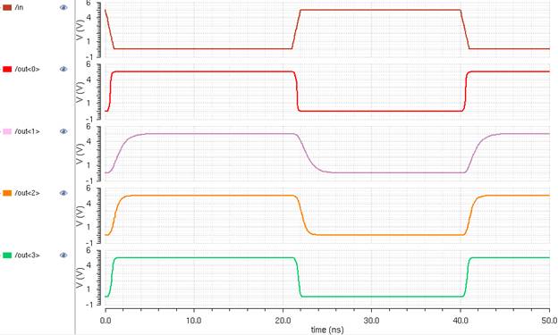
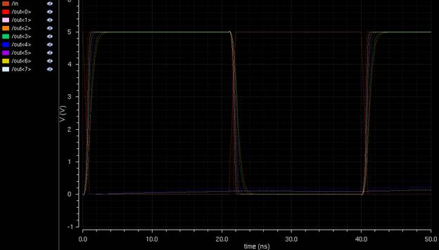
Show, in your lab report, how
a capacitive load influences the delay and rise/fall times.
Created schematics and
symbols for an 8-bit input/output array of: NAND, NOR, AND, inverter, and OR
gates.
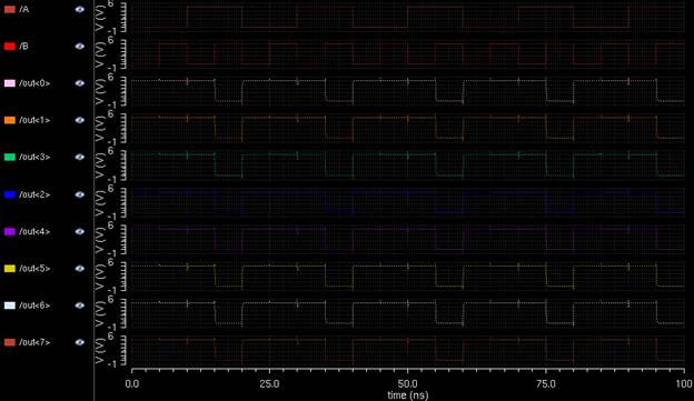
Also provided a few
simulation examples using these gates. To simplify the process, I made the
MOSFET equivalents of the NAND, NOR, and inverter gates. I would use the NAND
and NOR in conjunction with the inverter to create the schematics for the AND
and OR gates.
8-bit NAND:

8-bit NOR:

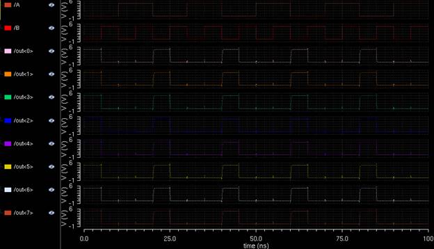
8-bit AND:

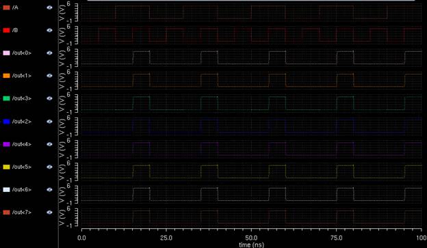
8-bit Inverter:

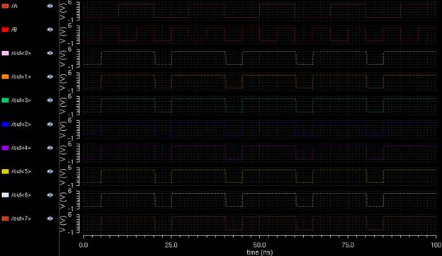
8-bit OR:

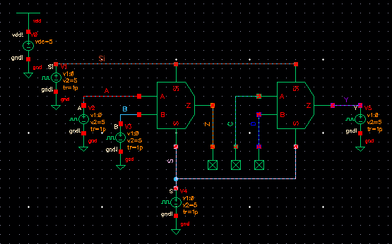
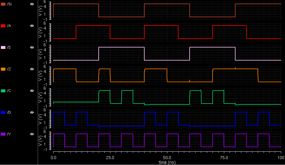
MUX Simulation:
A MUX is created using two transmission gates.
Neither transmission gate are on at the same time as the other. When S is 0,
the bottom PMOS is active, while the NMOS is not. When S is 1, it is opposite
where the top PMOS is active and the bottom NMOS is not. Si holds the opposite
value of S and is responsible for the triggering of the corresponding MOSFET.
When the top two MOSFETs are active, A is connected to the output. When the
bottom two MOSFETS are active, B is connected to the output.
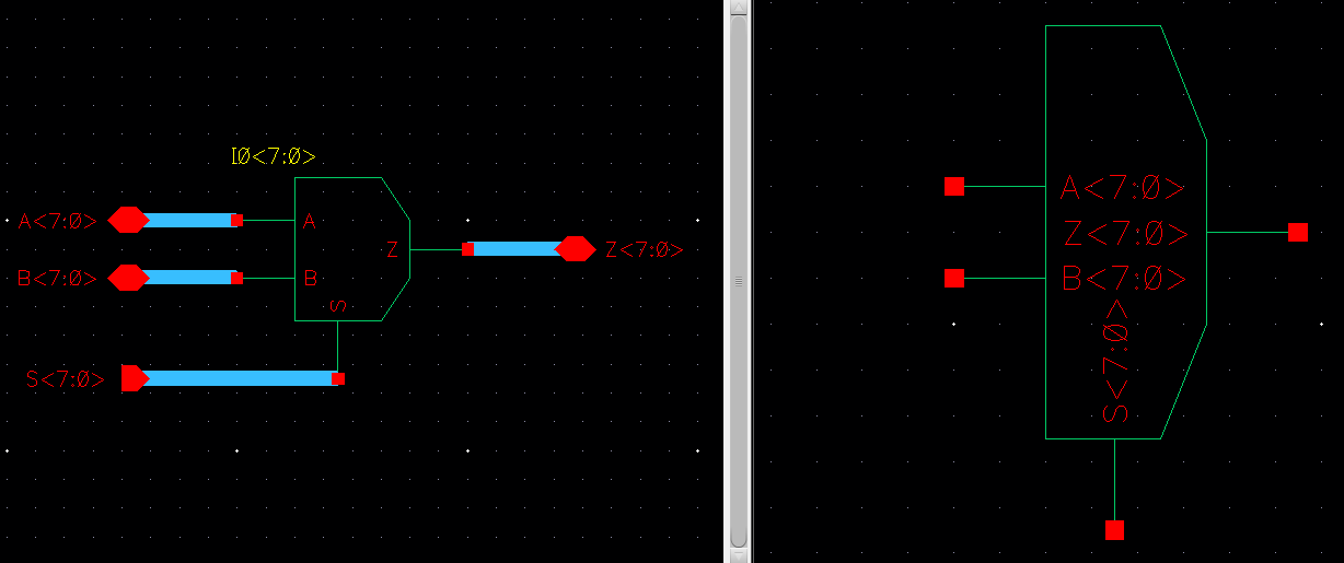
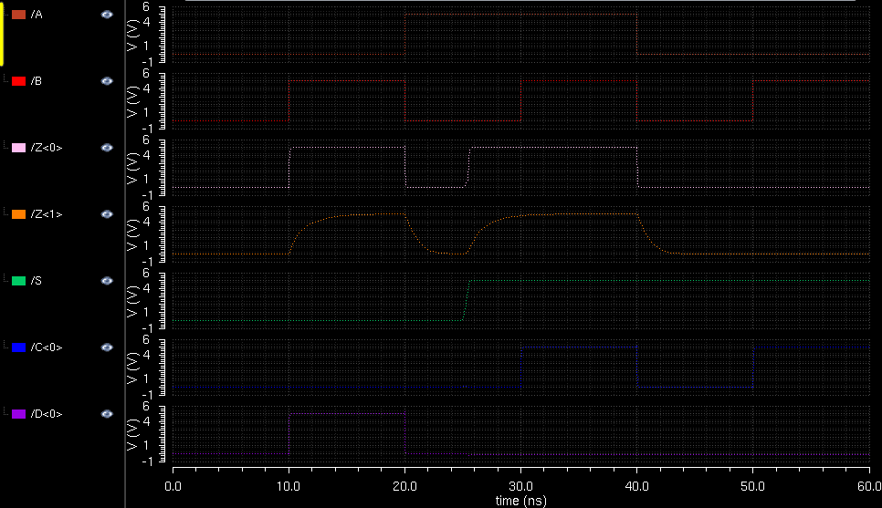
A demux is when you take the
S input of a mux, run it through an inverter, and connect the inverter’s output
to Si of the mux.
8-bit DEMUX:
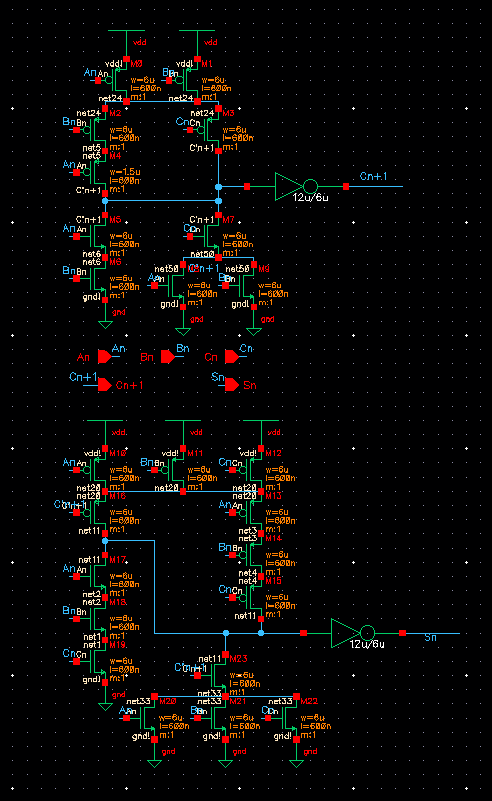
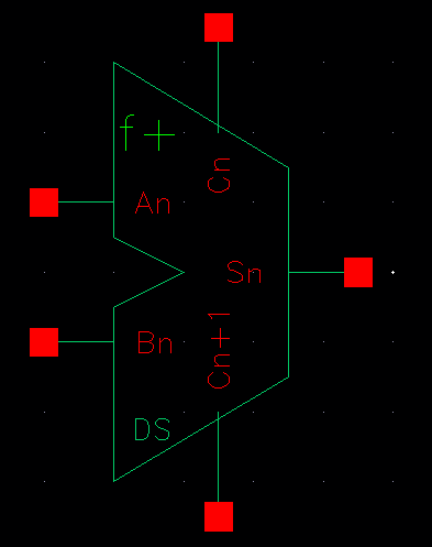
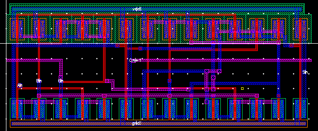
Drafted the schematic of a
full adder as shown in the book, then created a corresponding symbol and layout:
Using the Full Adder symbol,
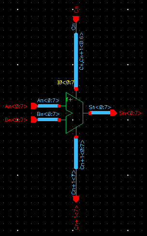
created the schematic for an 8-bit Full Adder, its layout, and its symbol:

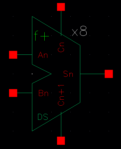
DRC LVS verification for
8-bit Full Adder:
![]()
