EE 421L – Digital IC Design Lab – Lab 5
Design, layout, and
simulation of a CMOS inverter
Author: Darryl Derico
E-Mail:
derico@unlv.nevada.edu
9/25/19
Lab Description:
The lab today is about
creating a CMOS inverter symbol and layout followed by simulating its
functionality.
Prelab:
Finished Tutorial 3:
Lab:
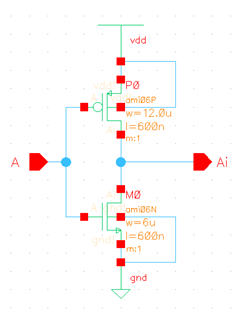
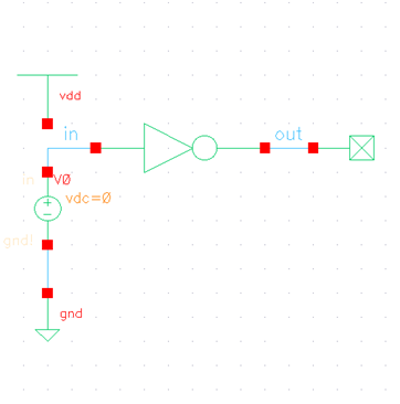
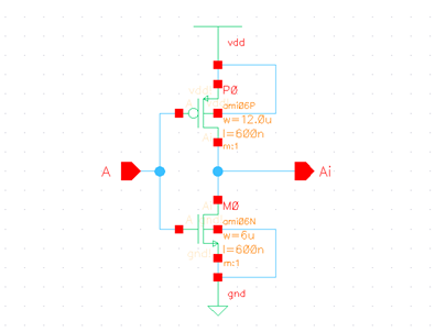
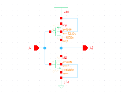
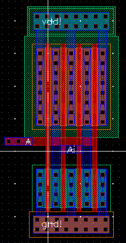
Created a schematic for an
inverter and an 4x inverter:
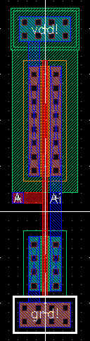
As well as their respective
symbols and layouts:
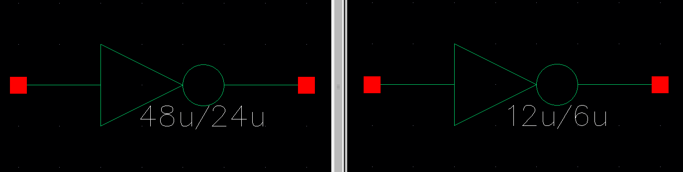
12u/6u: 48u/24u:
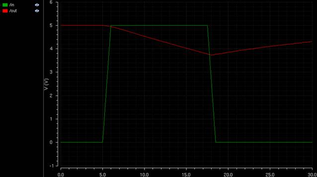
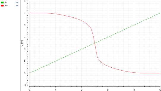
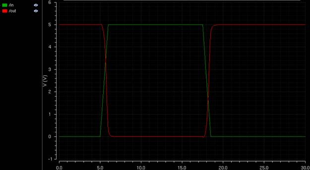
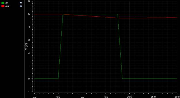
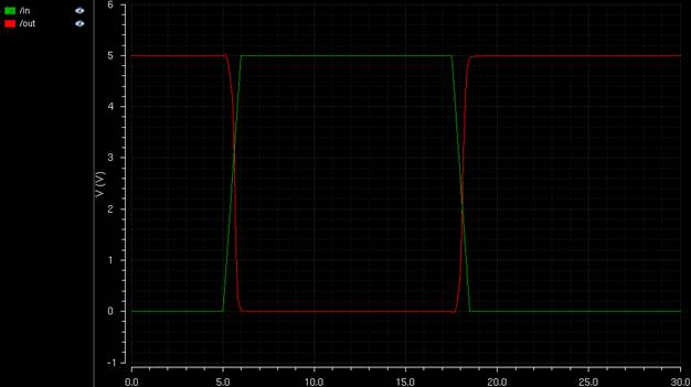
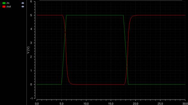
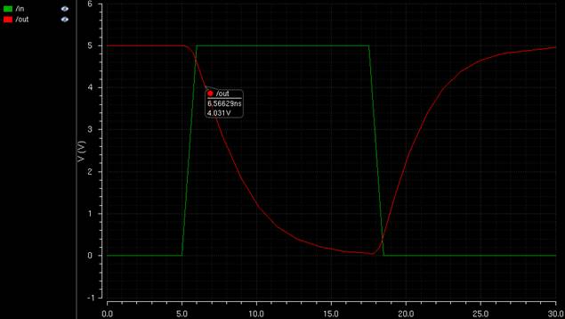
I then simulated both
inverters driving a 100fF, 1pF, 10pF, and 100pF capacitive load across both
inverters individually.
12u/6u Inverter simulations:
100fF:
1pF:
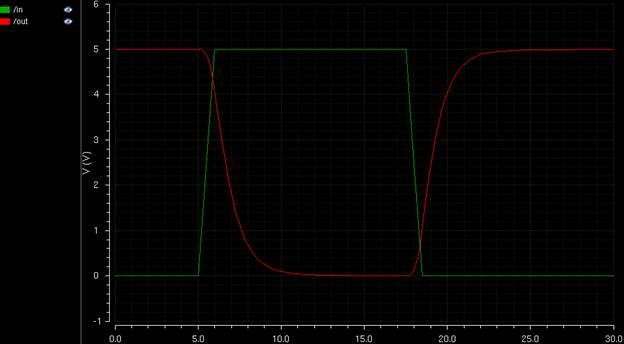
10pF:
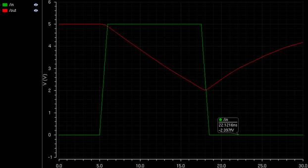
100pF:
48u/24u Inverter Simulations:
100fF:
1pF:
10pF:
100pF: