EE 421L – Digital IC Design Lab – Lab 4
IV characteristics and
layout of NMOS and PMOS devices in ON's C5 process
Author: Darryl Derico
E-Mail:
derico@unlv.nevada.edu
9/18/19
Lab Description:
For this lab, we are going
over the characteristics and layouts of both NMOS and PMOS devices in the C5
process.
Prelab:
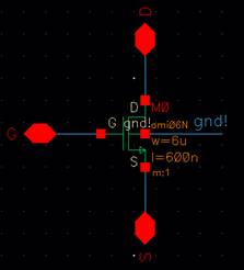
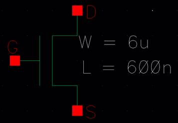
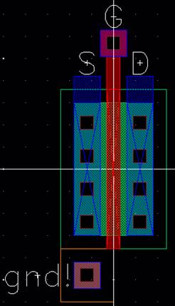
Finished Tutorial 2 resulting
in the creation of NMOS and PMOS schematics, symbols, and layouts as seen
below. Also performed the parametric analysis of their respective
schematics.
NMOS:
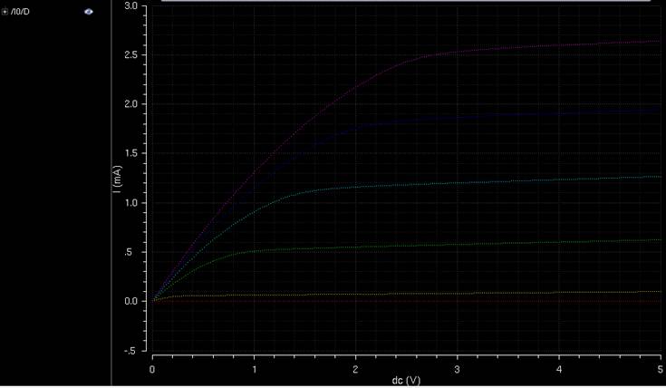
PMOS:
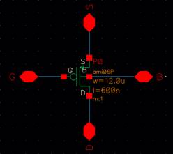

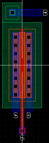
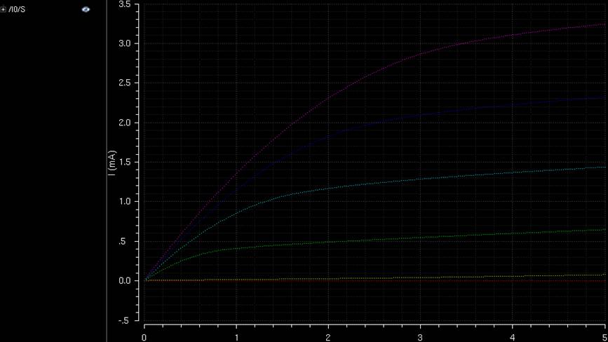
Lab:
For the first part, I
generated 4 schematics along with their corresponding simulations:
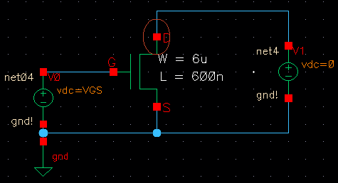
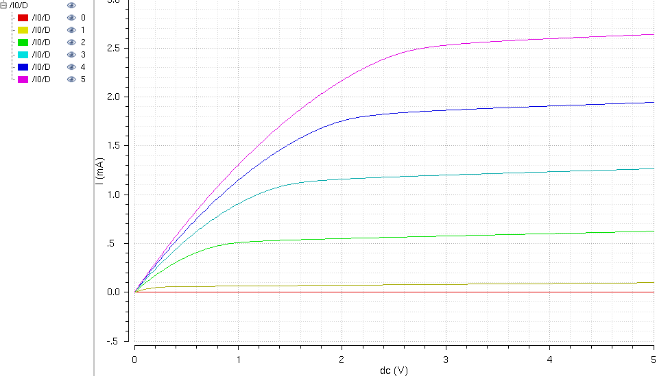
A schematic for simulating ID
v. VDS of an NMOS device for VGS varying from 0 to 5 V in 1 V steps while VDS
varies from 0 to 5 V in 1 mV steps. Use a 6u/600n width-to-length ratio:
![]()
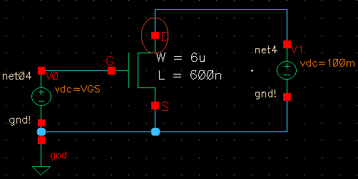
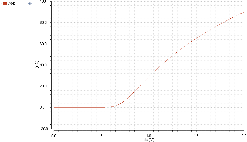
A schematic for simulating ID
v. VGS of an NMOS device for VDS = 100 mV where VGS varies from 0 to 2 V in 1
mV steps. Again use a 6u/600n width-to-length ratio:
![]()
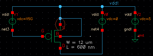
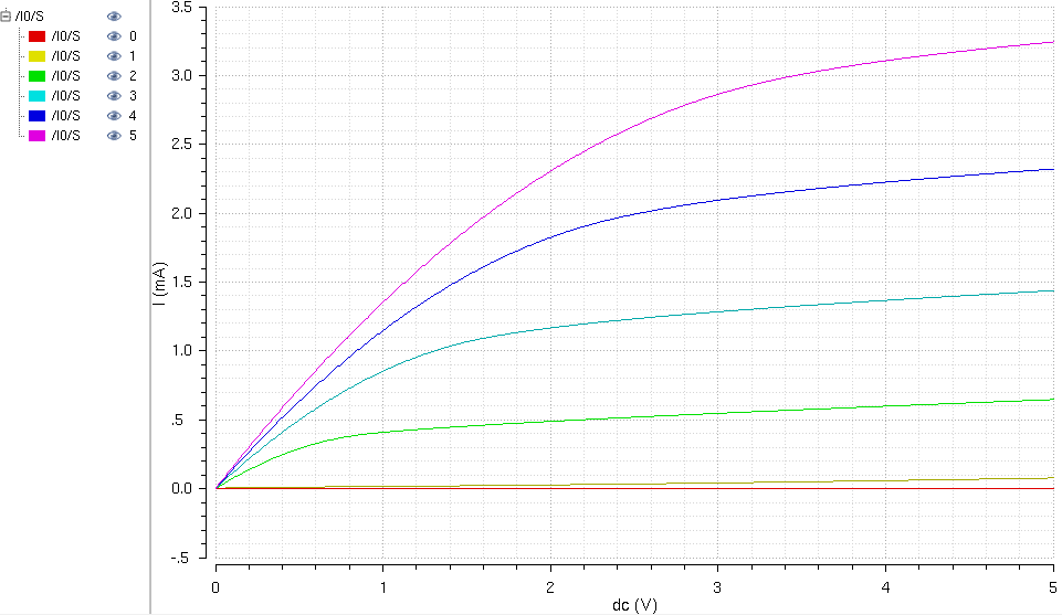
A schematic for simulating ID
v. VSD (note VSD not VDS) of a PMOS device for VSG (not VGS) varying from 0 to
5 V in 1 V steps while VSD varies from 0 to 5 V in 1 mV steps. Use a 12u/600n
width-to-length ratio:
![]()
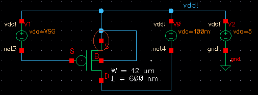
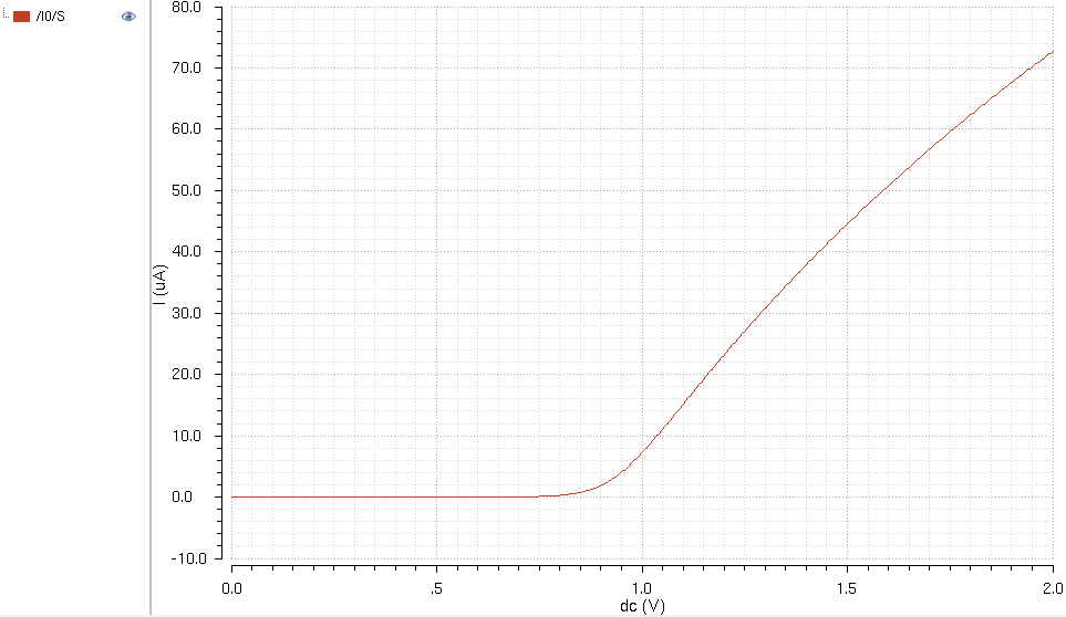
A schematic for simulating ID
v. VSG of a PMOS device for VSD = 100 mV where VSG varies from 0 to 2 V in 1 mV
steps. Again, use a 12u/600n width-to-length ratio:
![]()
Next, I had to make a layout
for a 6u/0.6u NMOS device and connect all its MOSFET terminals to probe pads.
Instead of downloading the zip file for the necessary parts, I decided to make
my own probe pads to get a little more practice with following MOSIS design
rules.
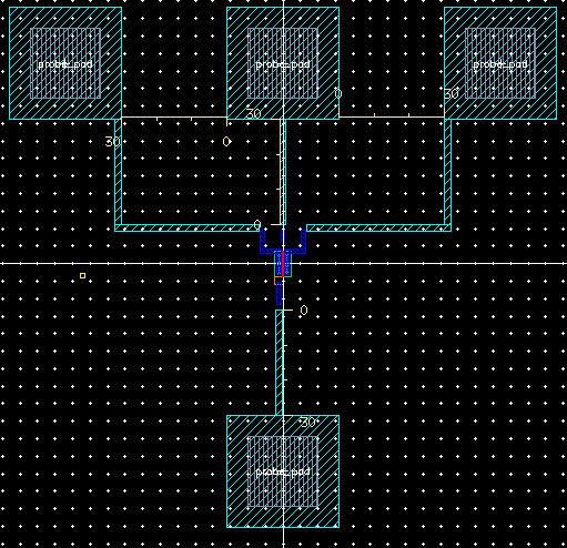
The layout passed DRC
verification.

After making a correlating
schematic, I verified the layout and schematic were the same with LVS.
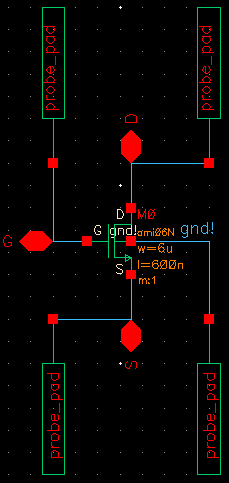

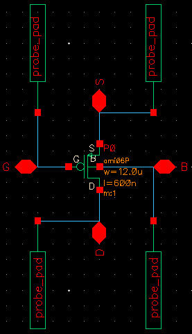
Lastly, I had to make the
layout of a PMOS device with all 4 of its MOSFET terminals connected to probe
pads like I did earlier with the NMOS.
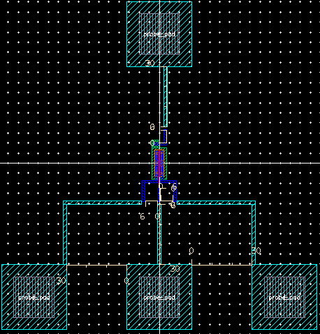
Then I verified the layout
with DRC.

After creating its
correlating schematic, the LVS confirmed that everything matches accordingly.
