EE 421L – Digital IC Design Lab – Lab 2
Design of a 10-bit
digital-to-analog converter (DAC)
Author: Darryl Derico
E-Mail:
derico@unlv.nevada.edu
09/04/2019
Lab Description:
For this lab, we are to
implement a 10-bit digital-to-analog converter (DAC) using n-well resistors.
Prelab:
ADC captures voltage at
specific time.
When ADC reads Vin, it is
converted into 10-bit binary number.
DAC then reads 10-bit binary
number, and outputs the voltage at increments equivalent to the LSB.
Downloaded and extracted
lab2.zip into the design directory.
![]()
Added statement to cds.lib.
![]()
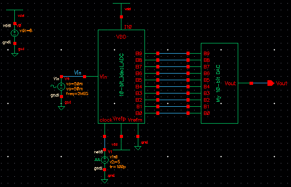
Opened the schematic view of
sim_Ideal_ADC_DAC.
Then launched ADE, loaded
cellview state, and pressed start to obtain stock schematic results.
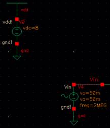
I altered the schematic to
change how the graph would appear and to further provide me with an
understanding of how Vout operates. Specifically, I changed Vdd to 8V and the
offset as well as the amplitude to 50mV. For analysis reasons, I also reduced
the tran analysis to 500 ns.
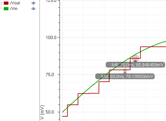
Simulating this provided me
with the following graph:
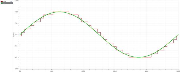
In terms of the stock schematic,
where Vdd=5V and N=10, the LSB=4.88mV. So at every 4.88 mV change in Vin, Vout
outputs the voltage at that time.
However, with my customized
parameters, the LSB would be 7.81mV.
This can be seen when
comparing the change from one interval of Vout to the next.
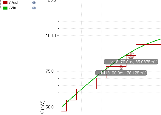
Calculating the difference in
voltage between the two points, 85.9375mV-78.125mV=7.8125mV. Thus, proving that
my LSB calculation is correct.
Lab:
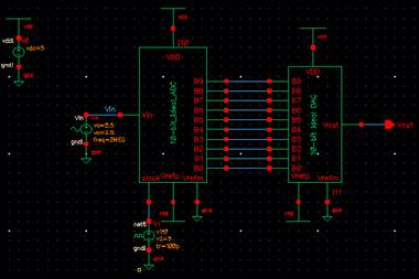
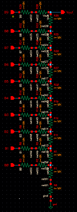
The first thing to do was design
a 10-bit Digital-to-Analog Converter using an n-well resistance of 10k ohms.
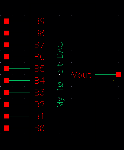
Additionally, I also modified
the original DAC symbol to reflect that of my personal DAC.
The output resistance of the
DAC can be determined by identifying parallel and series resistors as well as using
voltage division from the least significant bit and move upwards performing
voltage division until reaching Vout. If there are multiple inputs receiving voltage,
then one could use either superposition or Thevenin to calculate the voltage at
that source and repeat the voltage division process until Vout is determined.
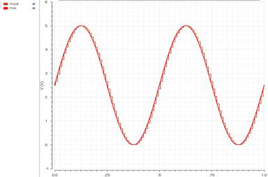
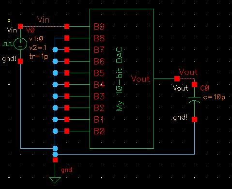
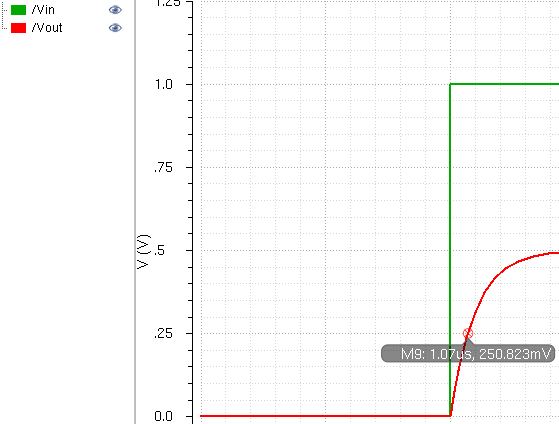
Here, I wanted to test the
delay of the DAC when driving a load, so I attached a voltage pulse source from
(0V to 1V) to B9 and added a 10pF capacitor to the load.
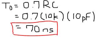
Using 0.7RC, we can predict
the delay the DAC has when driving a 10pF load.
R=10000
C=10*10-12
Td=0.7(10000)(10*10-12)=70ns=.07us
Finally, all that was left is
to place my DAC into the simulation in conjunction with the ADC to confirm its
functionality was correct.