EE 421L –
Digital IC Design Lab - Project
Authored by Chris Barr
Email: barrc1@unlv.nevada.edu
11/13/2019
Project
Goal:
Project (not a group effort, each student will turn in their own project)
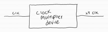
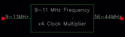
– design a circuit that takes a 9-11 MHz clock signal and generates a 36-44 MHz
clock signal. In other words, design x4 clock multiplier. The input clock is
multiplied by 4 and output. Assume the input clock signal has a 50% duty cycle.
Project
Requirements:
First half of the project (schematics and design discussions) of your
design and an html report detailing operation (including simulations), is due
at the beginning of lab on Nov. 13.
·
Your design report in html should show various input clock frequencies
and VDD voltages to show it works.
·
Put your report (proj.htm) in a folder called /proj
in your directory at CMOSedu and link to your
index.htm page.
·
Dr. Baker will go over your design with you (in person), including
running simulations, when lab meets on Nov. 13.
Second half of the project, a verified layout and documentation (in
html), is due at the beginning of lab on Nov. 20.
·
Dr. Baker will meet with you on Nov. 20 to go over your layout
·
Put your report in the /proj folder in your
directory at CMOSedu.
·
Ensure that there is a link on your project report webpage to your zipped
design directory.
Table of
Contents
First Half of Project (Schematic/Discussion)
-
1.) Design Planning/Sketching
-
2.) Component
Schematics/Symbols
-
3.) Final Design
Schematic/Simulations
Second Half of Project (Layout/Documentation)
-
4.) Component Layouts/Extracts
-
5.) Final Design
Layouts/Extracts
-
6.) Zipped Project
Folder (Download Link)
First Half
of Project (Schematic/Discussion):
The goal is to quadruple the clock signal input. What we have is one
input (9-11 MHz clock signal), and one output (36-44 MHz clock signal).
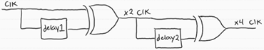
In order to multiply a 9-11 MHz clock signal, the use of digital logic
design can be implemented. Here’s an example of how we can multiply a clock
signal by utilizing an XOR gate.
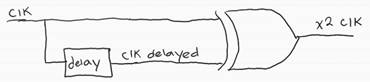 In this diagram, its
input will be a standard clock signal, and its output the doubled clock signal.
In this diagram, its
input will be a standard clock signal, and its output the doubled clock signal.
This technique is called edge detection and is what we will be using to
quadruple the clock signal.
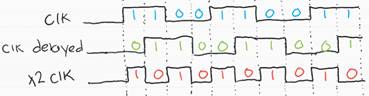 If we can manage to
push back the “clk delayed” by half of the duty
cycle, our result for “x2 clk”
If we can manage to
push back the “clk delayed” by half of the duty
cycle, our result for “x2 clk”
would appear as shown in the drawn-out waveform.
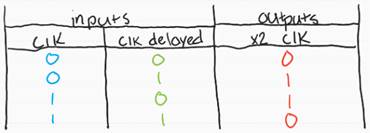 Here are the characteristics
of an XOR gate to prove that the waveform should act as drawn above.
Here are the characteristics
of an XOR gate to prove that the waveform should act as drawn above.
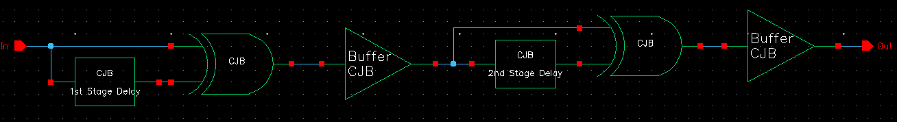
To quadruple our clock signal we’ll need two
different delay boxes, so our design will look like this:
 Each delay box will
have its own amount of time to delay because it will handle two different
frequencies.
Each delay box will
have its own amount of time to delay because it will handle two different
frequencies.
And to make these delay boxes, we will need inverters.
So, to finalize our design, we will need two different kinds of
components: XOR gates, and Inverters.
2.) Component
Schematics/Symbols
We need two components; XOR gate, and an inverter. But because we want to
create a longer delay, we want to increase the lengths of these inverters.
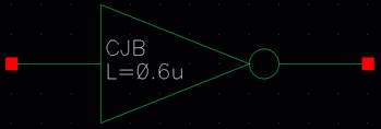
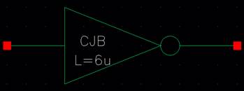
So, we’ll be making 3 kinds of inverters that are all 12u/6u with varying lengths.
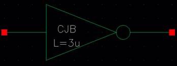
We’ll have inverters with lengths of 6u, 3u, and the minimum length of 0.6u
(600n).
|
|
Schematic |
Symbol |
|
Inverter (Length = 0.6u) |
|
|
|
Inverter (Length = 3u) |
|
|
|
Inverter (Length = 6u) |
|
|
|
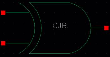
XOR Gate |
|
|
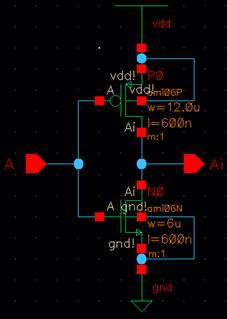
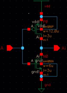
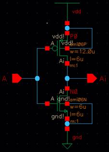
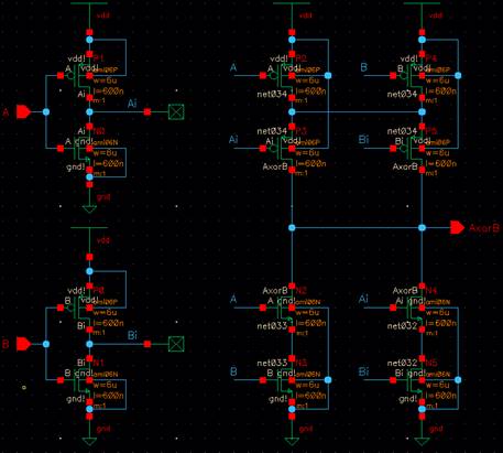
Inverter (Length = 6u), Inverter (Length = 3u), and Inverter (Length =
0.6u):
·
These components are used in the delay boxes.
·
The Inverter (Length = 0.6u) main purpose was used for the Buffer.
XOR Gate:
·
This is the main component that will help double the frequency.
Now that we have the smaller components created, we can condense them to
create the delay boxes and a buffer.
|
|
Schematic |
Symbol |
|
Buffer |
|
|
|
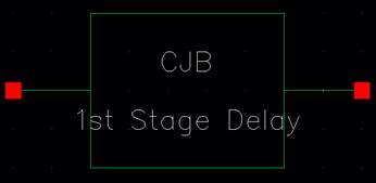
1st Stage Delay |
|
|
|
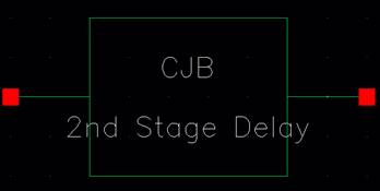
2nd Stage Delay |
(Click image to enlarge) |
|


Buffer:
·
We use two of the Inverters (Length = 0.6u) to square up the output
waveforms.
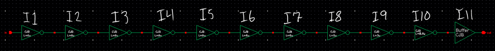
1st Stage Delay:
·
Using a clock input signal of 10 MHz (100ns period) as an example, this
delay box will delay the signal by roughly 25ns.
2nd Stage Delay:
·
Using a clock input signal of 10 MHz (100ns period) as an example, this
delay box will delay the signal by roughly 12.5ns.
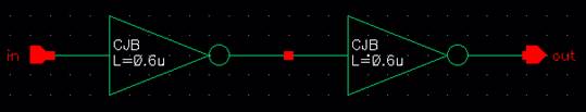
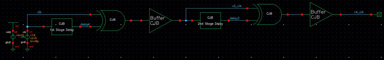
3.) Final Design
Schematic/Simulations
Putting all the components together as planned, this is what our final
schematic and symbol looks like.
Proceeding to the detailed simulation of the x4 Clock Multiplier. This is
the setup that will test every point in the schematic.
Tabulated Results of the Simulations:
Note: Click image to enlarge
|
|
Frequency = 9 MHz |
Frequency = 10 MHz |
Frequency = 11 MHz |
|
VDD = 4.5V |
|
|
|
|
VDD = 5V |
|
|
|
|
VDD = 6V |
|
|
|
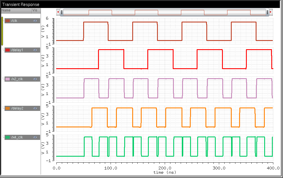

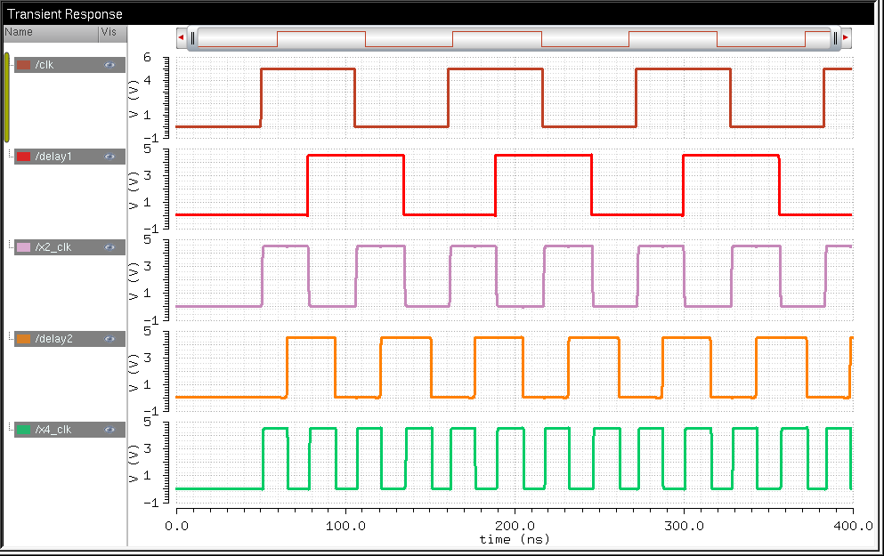
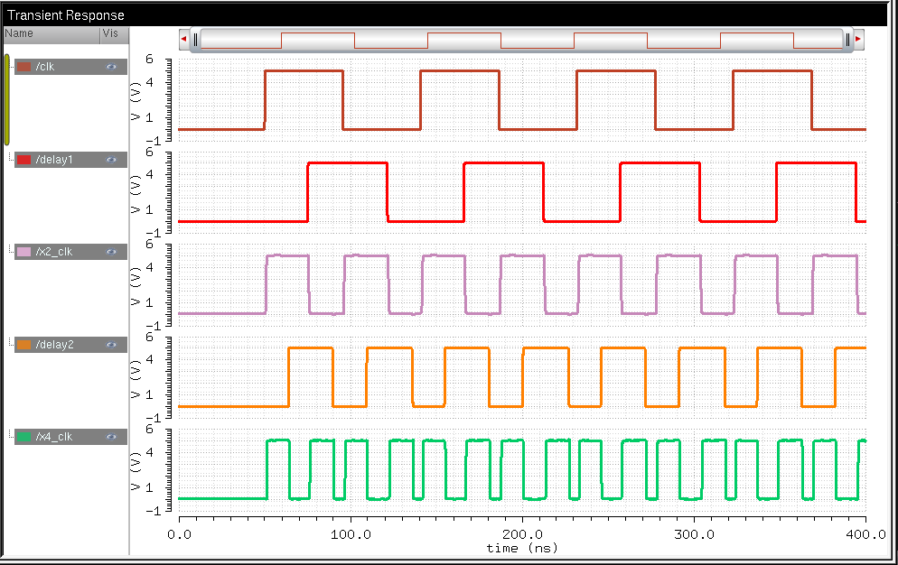
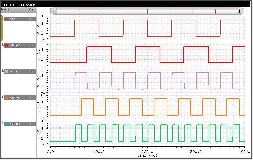

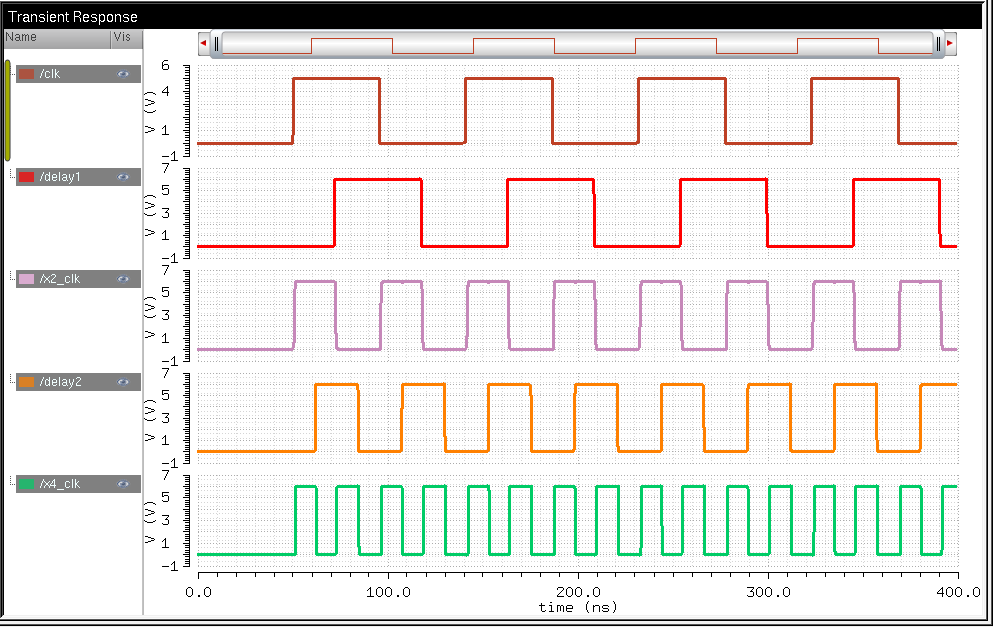
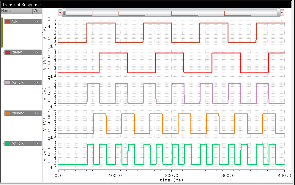
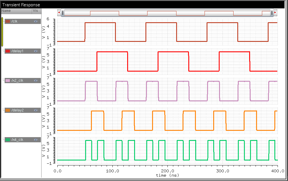
What we can notice is that at different Frequency values, we will get an
offset on our x4 clock signal and narrow the periods.
When we raise or decrease VDD it will raise or decrease the
amplitude of our x4 clock signal.
Notice that the further away the frequency and VDD get from 10
MHz and 5V (respectively), the output of the ‘x4_clk’ will cause a major
glitch. This is shown on the image of VDD = 4.5V and Frequency = 9 MHz.
Second Half
of Project (Layout/Documentation):
4.) Component Layouts/Extracts
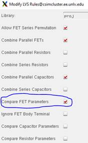
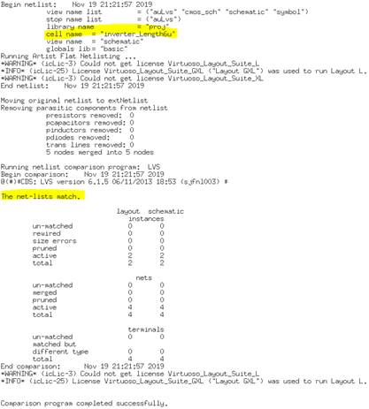
To ensure that our layouts match our schematics, we will be modifying the
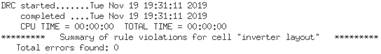
default LVS rules:
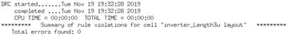
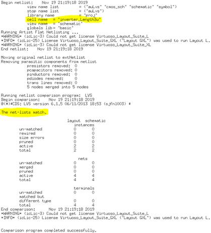
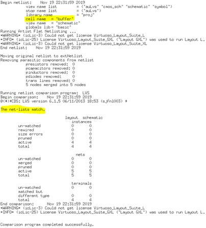
Tabulated Components Layout and Extracted views with DRC/LVS
Verification:
|
|
Layout |
Extracted |
DRC Verified |
LVS Verified |
|
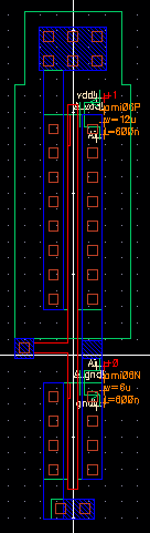
Inverter (Length =
0.6u) |
|
|
|
|
|
Inverter (Length =
3u) |
|
|
|
|
|
Inverter (Length =
6u) |
|
|
|
|
|
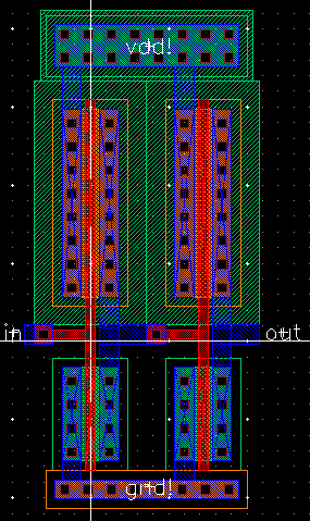
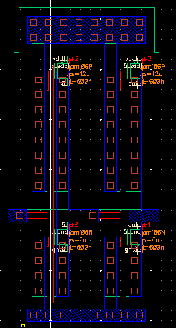
XOR Gate |
(Click image to
enlarge) |
(Click image to
enlarge) |
|
|
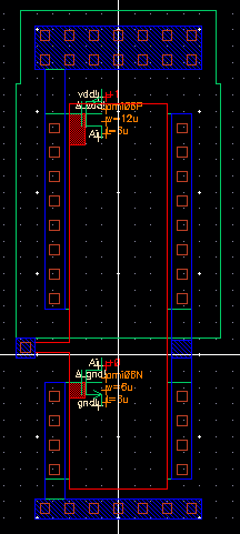

Tabulated Large Components Layout and Extracted:
|
|
Layout |
Extracted |
|
Buffer |
|
|
|
1st
Stage Delay |
|
|
|
2nd
Stage Delay |
(Click image to
enlarge) |
|
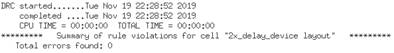
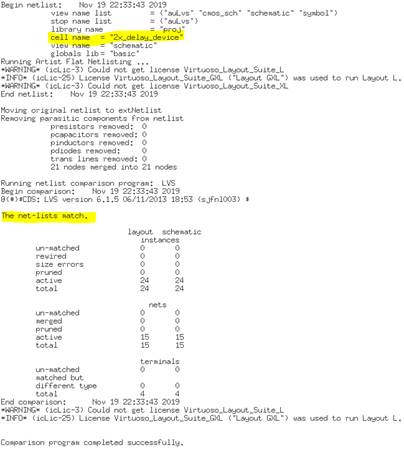
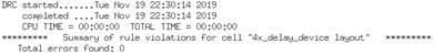
Tabulated Large Components DRC/LVS Verification:
|
|
DRC Verified |
LVS Verified |
|
Buffer |
|
|
|
1st
Stage Delay |
|
|
|
2nd
Stage Delay |
|
|

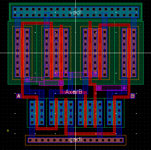
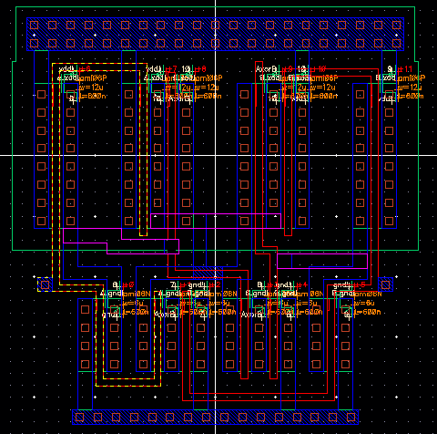
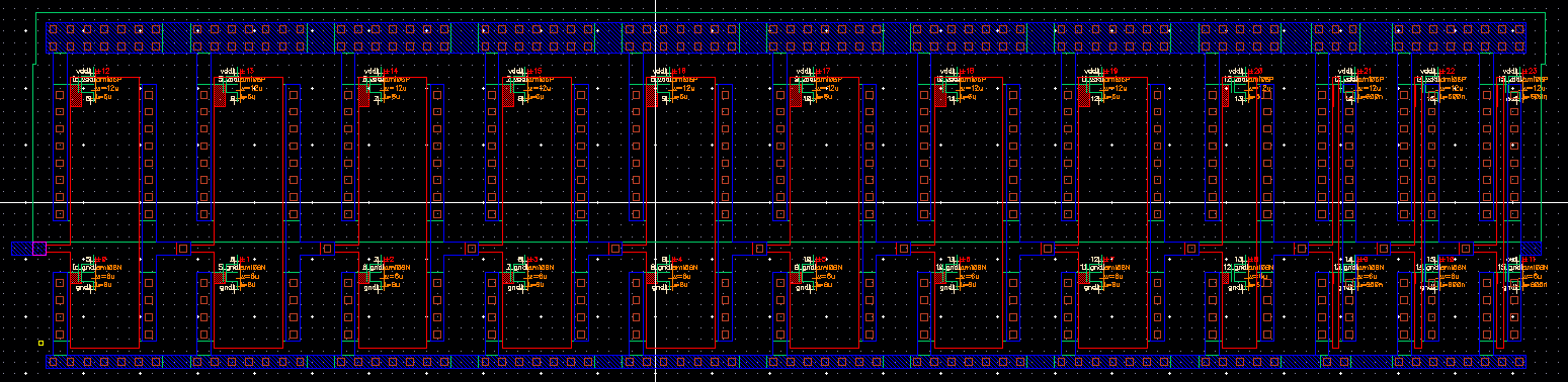
5.) Final Design
Layouts/Extracts
Now that all the designs are modulated and verified, the final design can
easily come together.
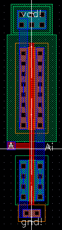
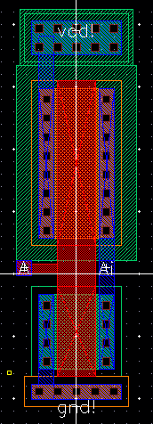
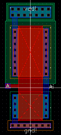
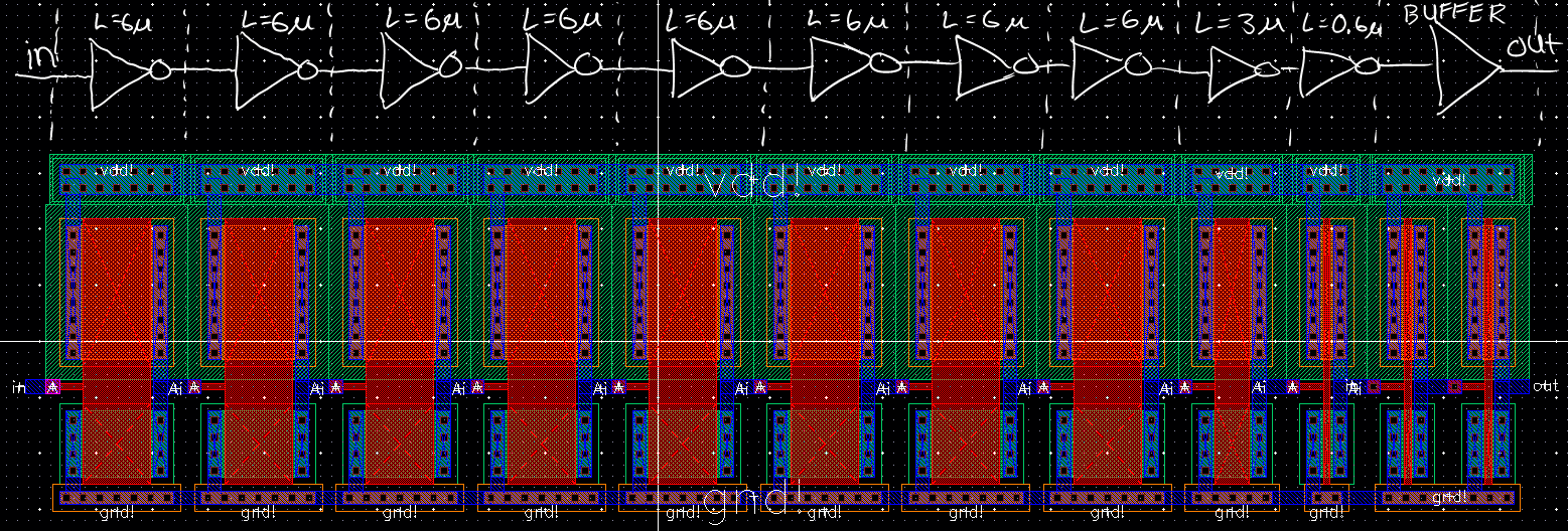
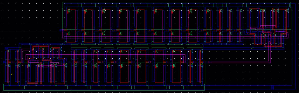
Layout view:
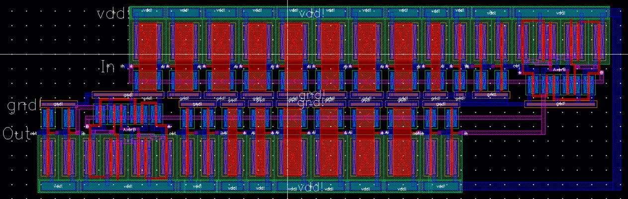
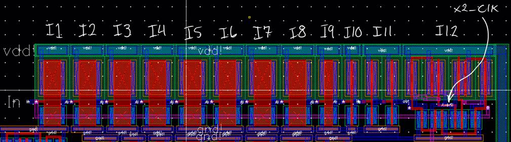
The top half of the layout represents the ‘x2_clk’.
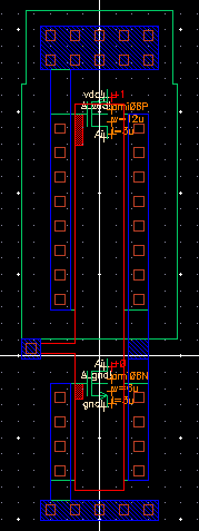
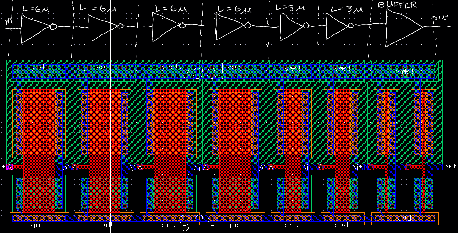
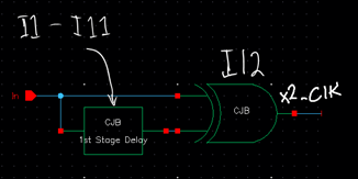
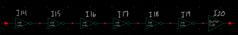
Below is a labeled schematic of the instantiations within the ‘1st
Stage Delay’ box.
Below is a labeled schematic of the first half of the final design
schematic.
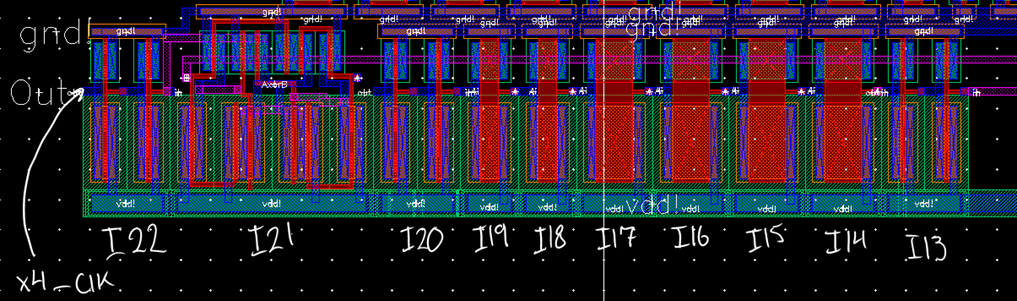
Below is a labeled layout of the top half of the final design layout to
make clarity of the matching schematic.
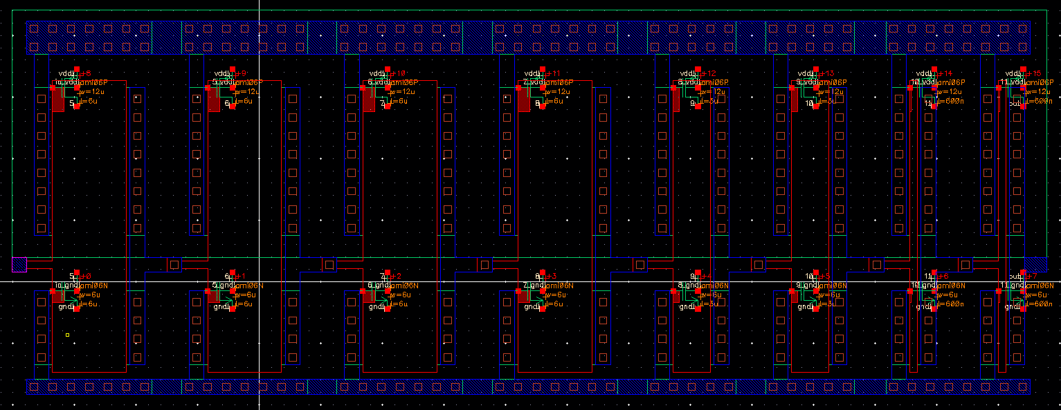
The bottom half of the layout represents the ‘x4_clk’.
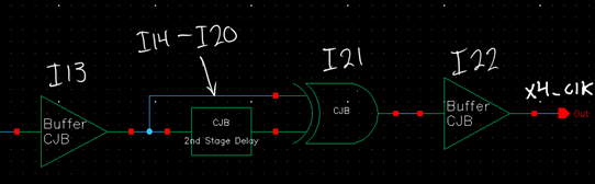
Below is a labeled schematic of the instantiations within the ‘2nd
Stage Delay’ box.
Below is a labeled schematic of the second half of the final design
schematic.
Below is a labeled layout of the top half of the final design layout to
make clarity of the matching schematic.
Extracted view:
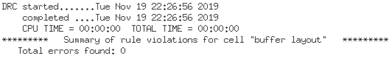
DRC Verified:

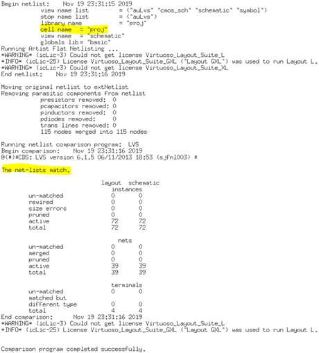
LVS Verified:
6.) Zipped Project Folder
(Download Link)

Left-click image to download the FULL .zip of this project.