EE 421L –
Digital IC Design Lab - Lab 7
Authored by Chris Barr
Email: barrc1@unlv.nevada.edu
11/06/2019
Zipped Lab7
folder:
lab7_cjb.zip
Lab
Description:
This lab we’ll be using buses and arrays in the design of word inverters,
muxes, and high-speed adders.
Prelab
For this prelab, we’ll be following Tutorial 5
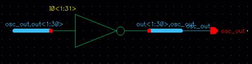
After creating a ring oscillation with 31 inverters, we deleted them all
and created a bus for the inverter to fit 31 bits
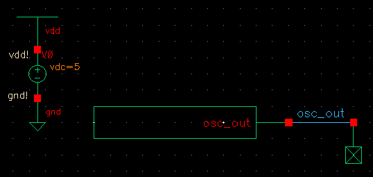
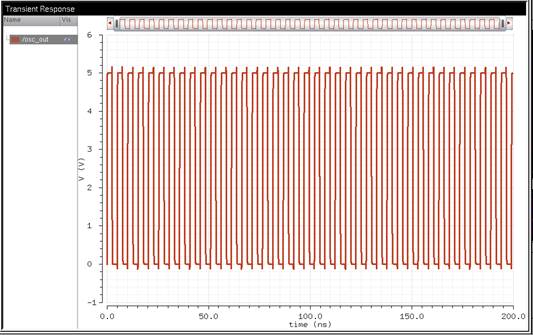
With this setup, we could then create the sim schematic to test it out,
and with it came this result
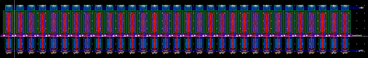
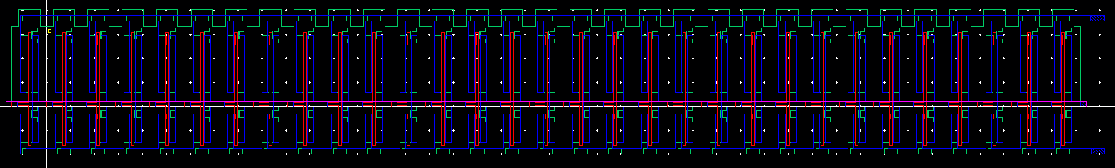
Now that we know our schematic works, we move onto the layout and
extractive view
And to test our layout for validity, we DRC and LVS it
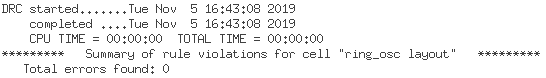
This ends Tutorial 5
Lab
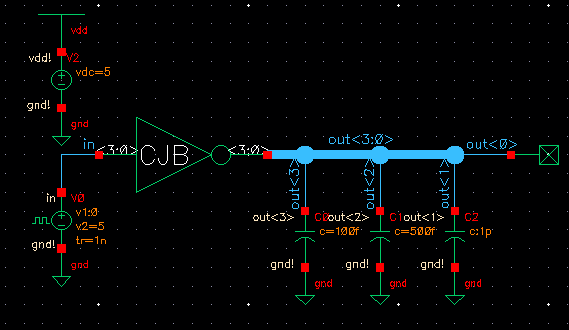
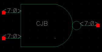
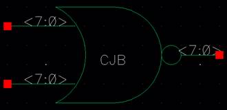
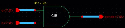
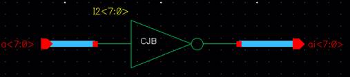
We can make an equivalent circuit to the image below using buses
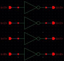
This is the equivalent circuit; it uses wide wire with a 4-bit input and
output named b<3:0> and bi<3:0> respectively
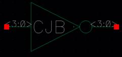
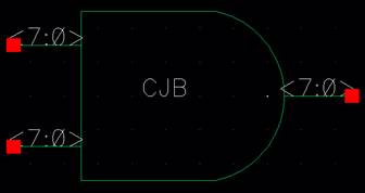
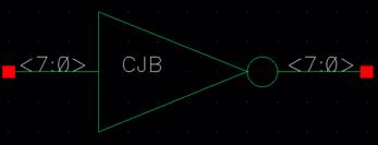
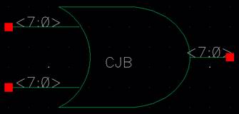
The symbol we’ll be using for it
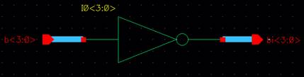
This is the simulation schematic we’ll be using to test it, 100fF on the
4th bit, 500fF on the 3rd bit, 1pF on the 2nd
bit, and a noConn on the 1st bit
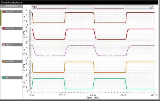
Our results are shown to the right of the schematic
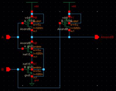
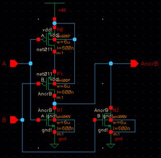
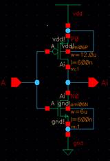
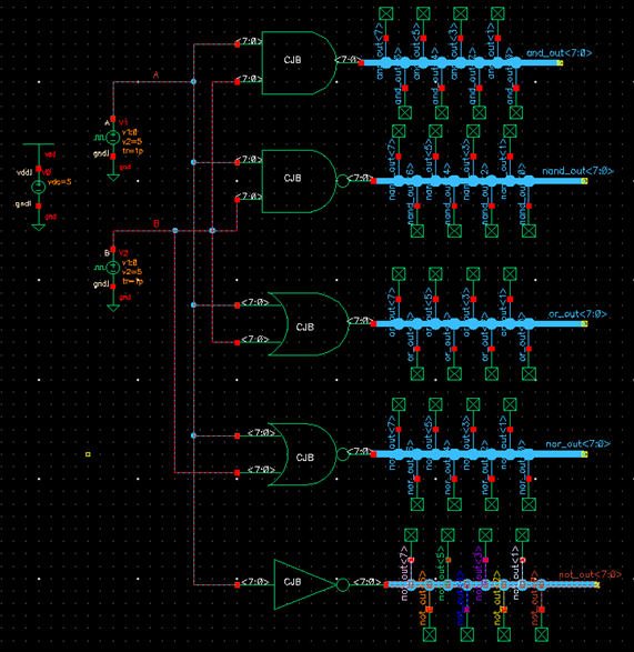
Now we’ll create schematics and symbols for an 8-bit input/output array
of: NAND, NOR, AND, inverter, and OR gates.
|
|
1-bit, Schematic |
8-bit modified, Schematic |
Symbol |
|
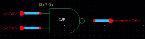
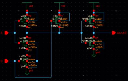
8-bit NAND Gate |
|
|
|
|
8-bit NOR Gate |
|
|
|
|
8-bit AND Gate |
|
|
|
|
8-bit Inverter Gate |
|
|
|
|
8-bit OR Gate |
|
|
|
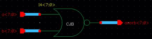
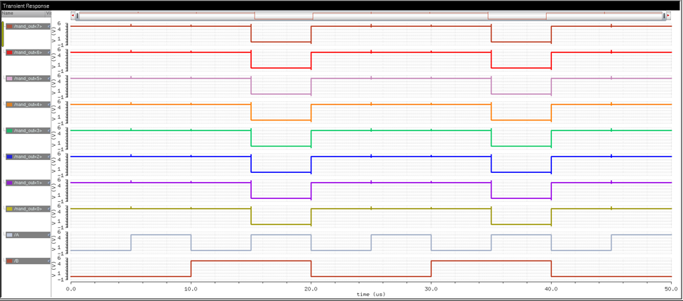
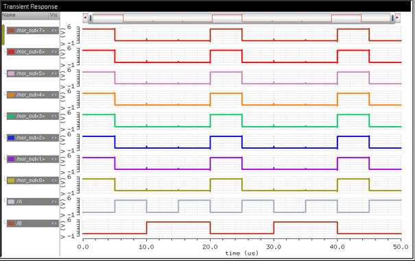
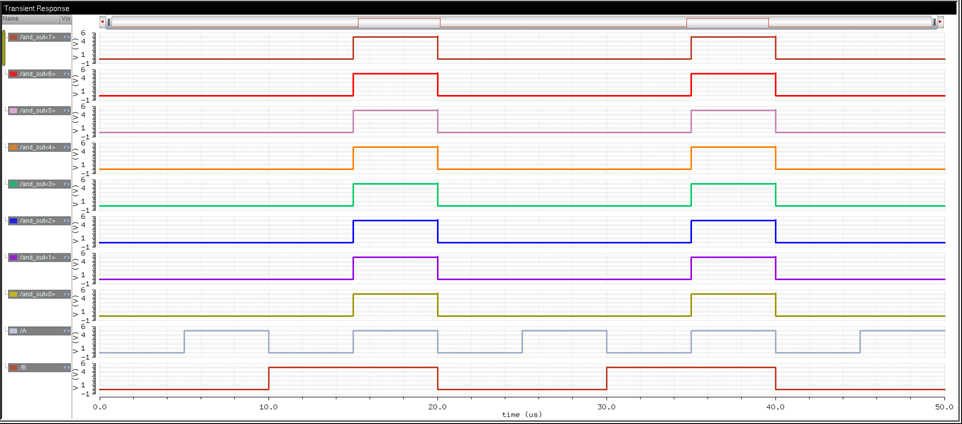
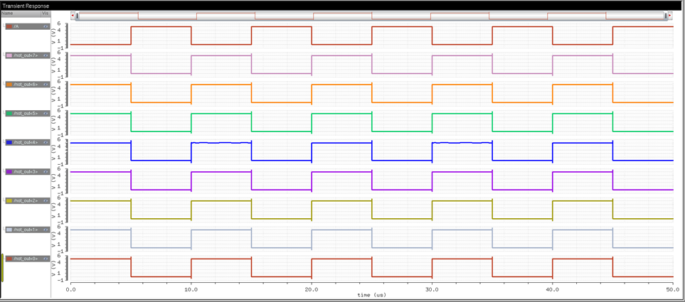
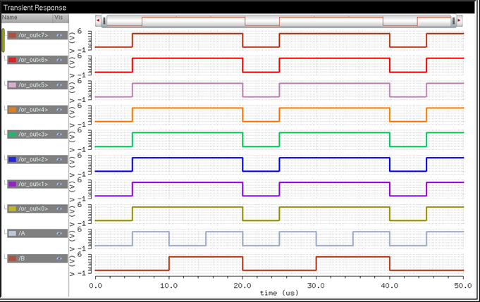
This is the simulation schematic we’ll be going with, as well as the
results it came with
|
|
Simulation Results |
|
8-bit NAND Gate |
|
|
8-bit NOR Gate |
|
|
8-bit AND Gate |
|
|
8-bit Inverter Gate |
|
|
8-bit OR Gate |
|
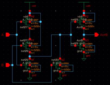
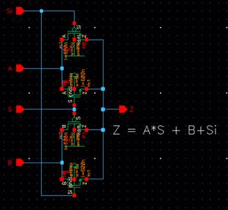
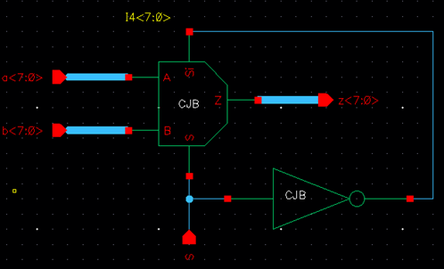
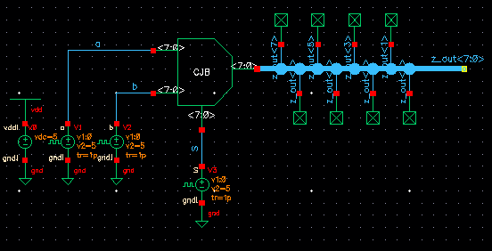
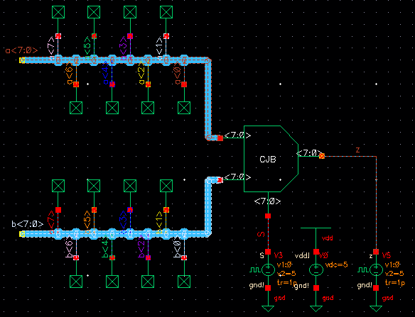
Now we’ll be drawing up a schematic for a 2-to-1 DEMUX/MUX, creating the
symbol, and simulating it
Afterwards, we’ll create a 8-bit bus for it and create
the symbol for that as well as simulate it
Note: For the 8-bit DEMUX/MUX, I did invert the input of the S and wired
it to the Si within the 8-bit schematic itself. It’s apparent as to when you
see the symbol and onwards that there is no Si input attached.
|
|
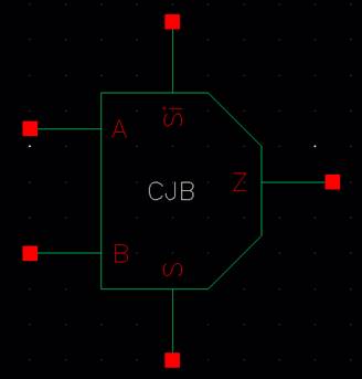
1-bit, DEMUX/MUX |
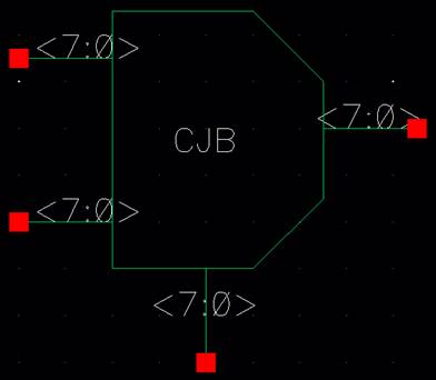
8-bit, DEMUX/MUX |
|
Schematic |
|
|
|
Symbol |
|
|
|
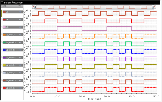
Simulation
Schematic |
|
|
|
Simulation Results |
|
|
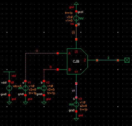
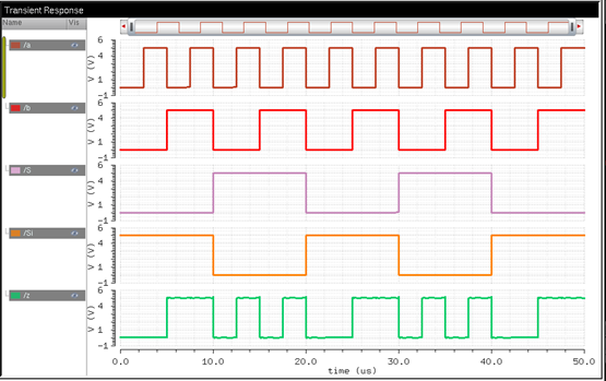
Just to show that the MUX does act as a DEMUX too, here’s the simulation
schematic and result to alongside it
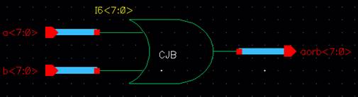
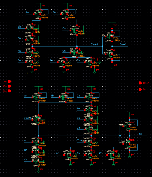
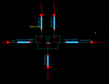
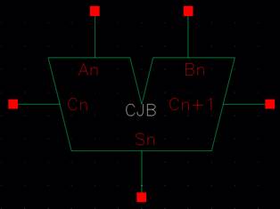
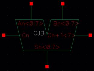
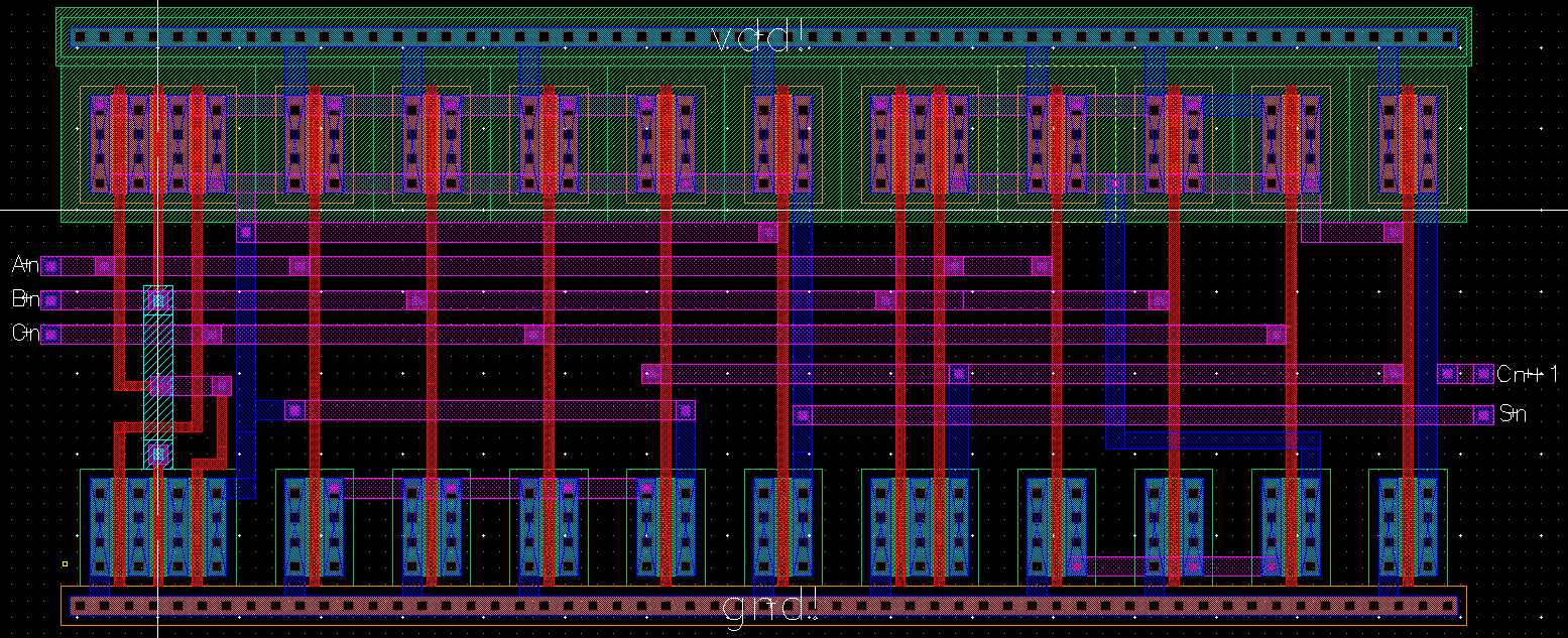
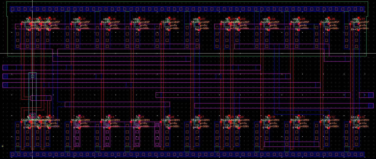
Finally, we’ll draft the schematic of the full-adder seen in Fig. 12.20
(CMOS 4th edition) using 6u/0.6u devices (both PMOS and NMOS). Create
an adder symbol for this circuit (see the symbol used in lab6). Use this symbol
to draft an 8-bit adder schematic and symbol. And then simulate the operation
of the 8-bit adder.
|
|
1-bit, Full-Adder |
8-bit, Full-Adder |
|
Schematic |
|
|
|
Symbol |
|
|
|
Layout |
|
|
|
Extracted |
(left-click picture to enlarge) |
|
|
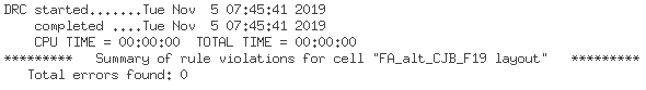
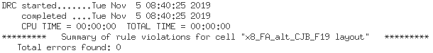
DRC Verification |
|
|
|
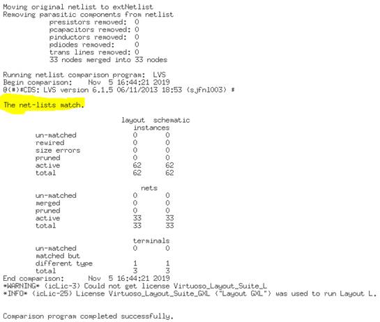
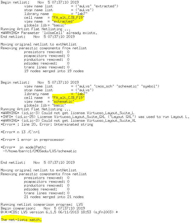
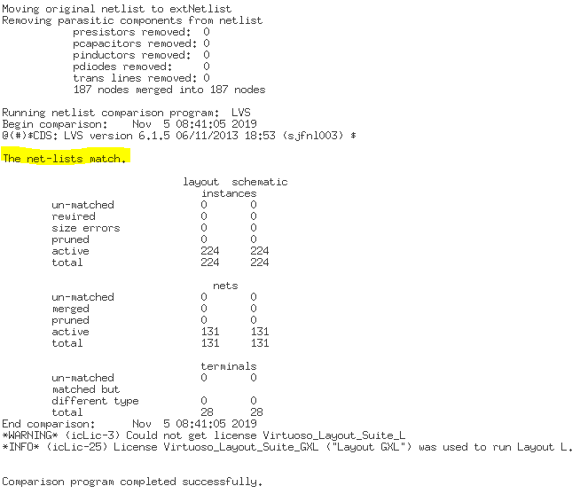
LVS Verification |
|
|
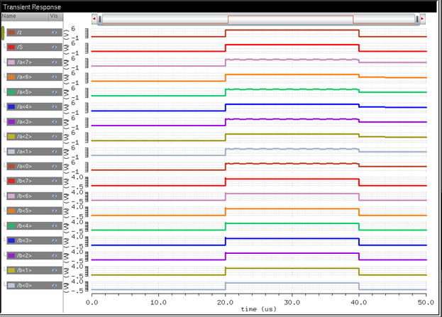
Now we simulate the 8-bit Full-Adder to make sure we created it correctly
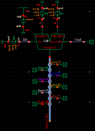
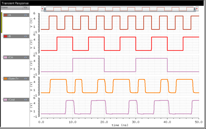
We can just take the last value of the sum, and we’ll notice that it
matches alongside the cout with the given inputs.
I will be backing up my labs on Google Drive, as per usual: