EE 421L –
Digital IC Design Lab - Lab 6
Authored by Chris Barr
Email: barrc1@unlv.nevada.edu
10/23/19
Zipped Lab6
folder:
lab6_cjb.zip
Lab
Description:
Design, layout, and simulation of a CMOS NAND gate, XOR gate, and
Full-Adder.
Prelab
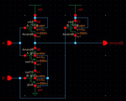
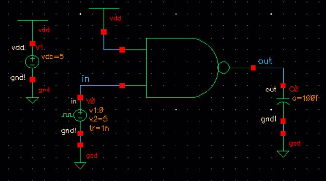
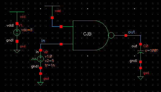
Following Tutorial 4, I will be creating the NAND gate
This is the schematic created, using 2 PMOS’ and 2 NMOS’ in the
construction of the NAND gate
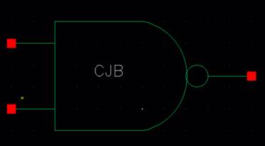
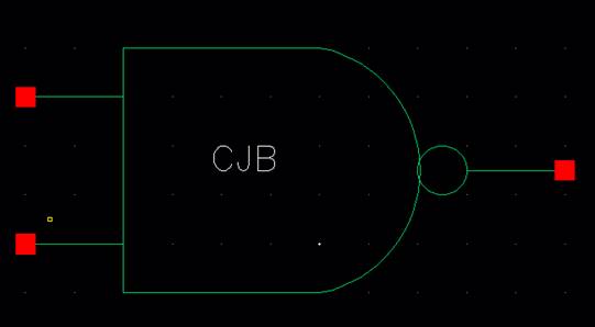
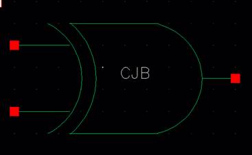
To represent the design of the NAND gate, I drew out this symbol
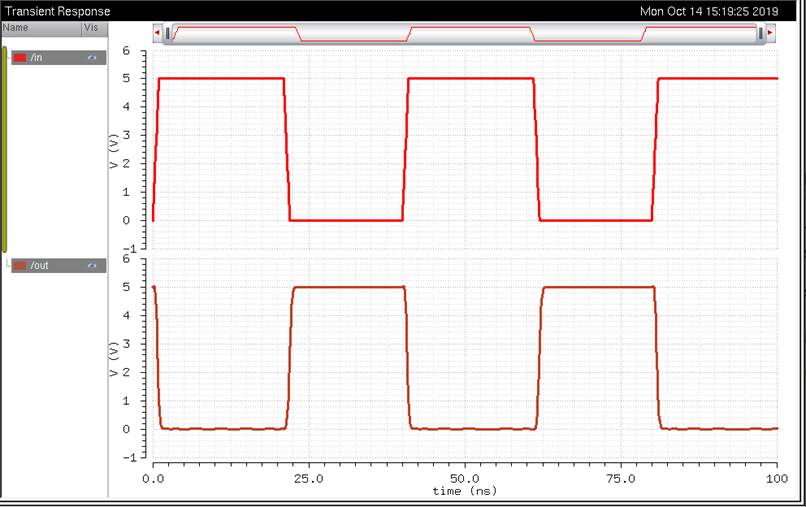
Now to confirm the functionality of this constructed NAND gate, I will
simulate it to check its results
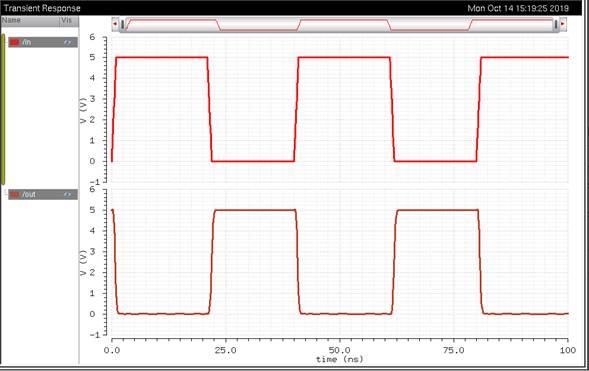
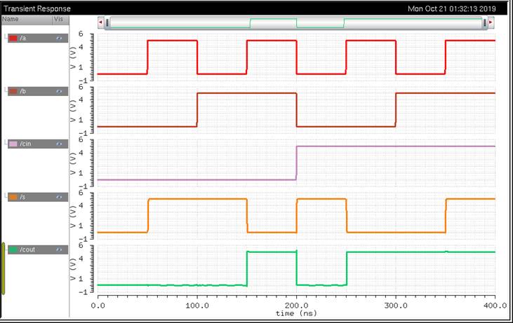
The NAND gate is fully functional, we can continue to the layout design
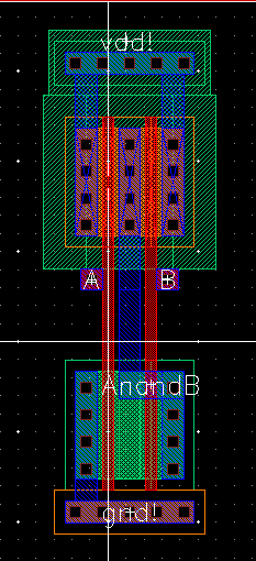
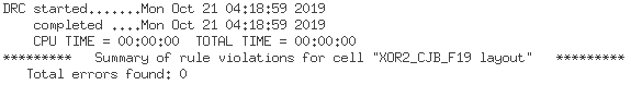
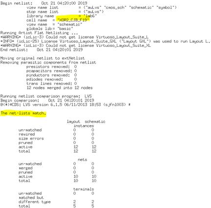
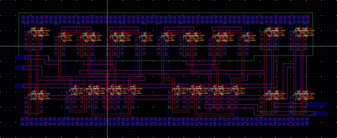
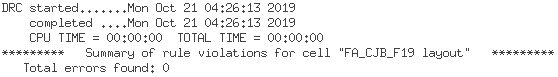
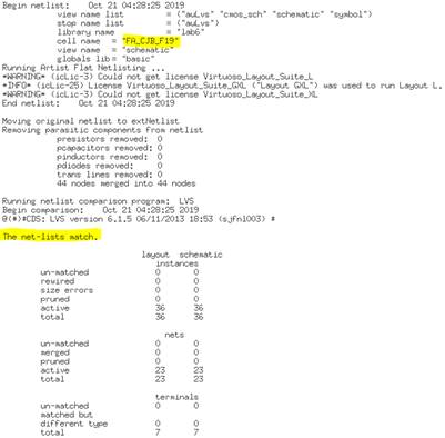
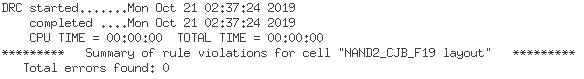
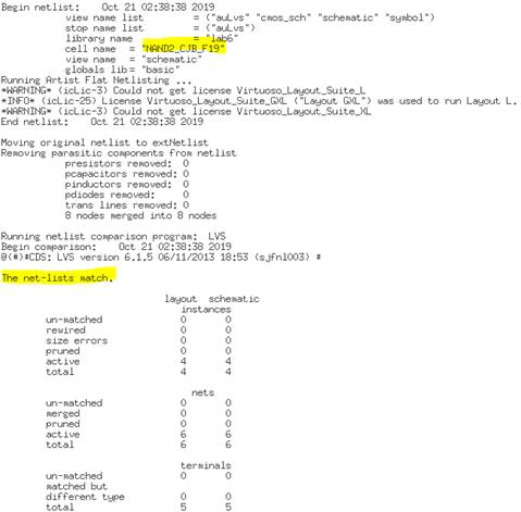
To prove the designs completion, we’ll use DRC and LVS verification
DRC Verification
LVS Verification
This ends the tutorial 4. We achieved creating the NAND gate.
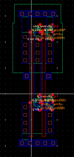
Note: At the end of the tutorial, we obtained an error of a “width
mismatch”.
The error was not received here
because I had fixed the width in the layout. This can be seen in the above
picture.
Lab
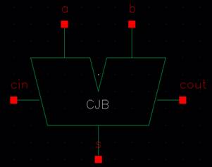
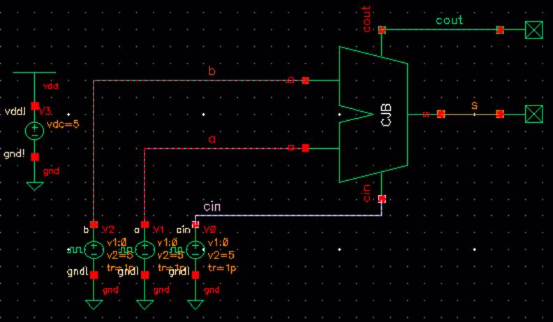
This lab will task us to create a Full-Adder, which we know uses 2 XOR
gates, and 2 NAND gates. This can be seen below.
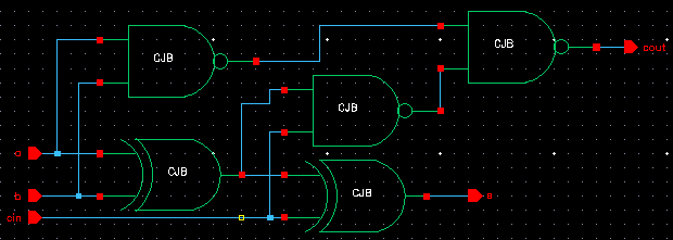
So, in order to achieve the Full-Adder, we’ll need to construct a NAND
gate, and an XOR gate.
The NAND gate had already been created prior, due to the prelab (Tutorial 4).
But here’s the details of the construction, in case you forgot.

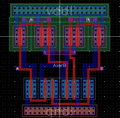
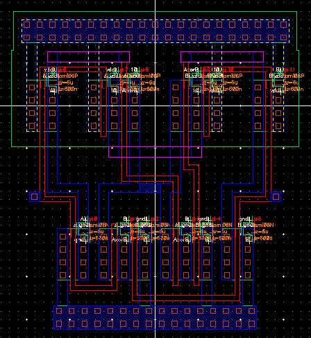
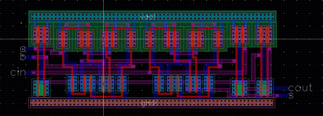
We can move on to the construction of the XOR gate. This won’t be as
simple as the previous construction, the NAND gate. We’ll need 6 PMOS’ and 6
NMOS’.
All the PMOS’ and NMOS’ will be the same size. Width = 6u, Length = 600n.
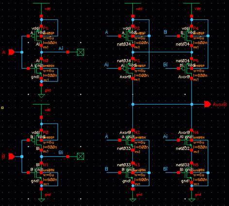
And to represent the XOR gate design
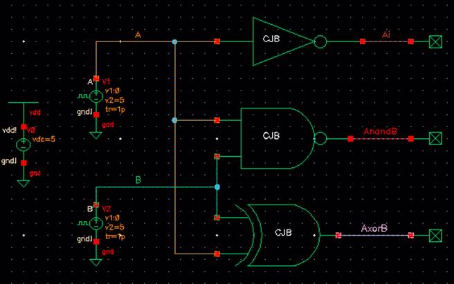
To prove that our schematic is functional, we’ll place it in a
simulation. We’ll also add the simulations of a NOT gate and NAND gate next to
our XOR gate.
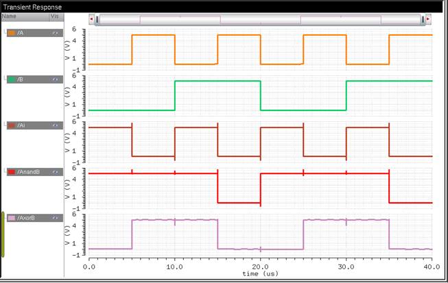
The simulation shows glitches on all of the outputs. In digital design,
we call these hazards. What we are witnessing are actually called Static
Hazards.
Static Hazards take place when there’s a change in the input that causes the
output to momentarily change before stabilizing it to the correct value.
It’s possible to fix these static hazards by introducing more logic gates to
the circuit to create enough time (slack) for the output to stabilize the
value.
Here are the truth tables for all three gates, that way it can be viewed
side-by-side to the simulation to prove it’s correct.