EE 421L –
Digital IC Design Lab - Lab 5
Authored by Chris Barr
Email: barrc1@unlv.nevada.edu
10/09/19
Zipped Lab5
folder:
lab5_cjb.zip
Lab
Description:
This lab we will be going over making a CMOS inverter. We will be using a
12um/6um CMOS inverter, and a 48u/24u CMOS inverter.
Prelab
For the prelab, I will be following Tutorial 3 to design, layout, and
simulate a CMOS inverter.
First, we’ll create a new library called Tutorial 3, and create a new
cell for the schematic of the inverter.
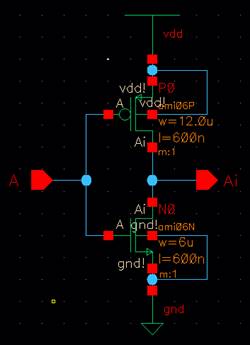
With the pins labeled A (input) and Ai (output), we can move onto making
the symbol.

And then create the layout, alongside extracting it. I DRC/LVS verified
my layout.


Created my sim schematic that included my symbol.
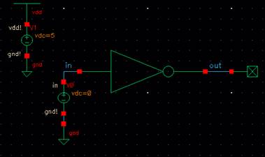
And then I simulated to check the result. This is what it looks like:
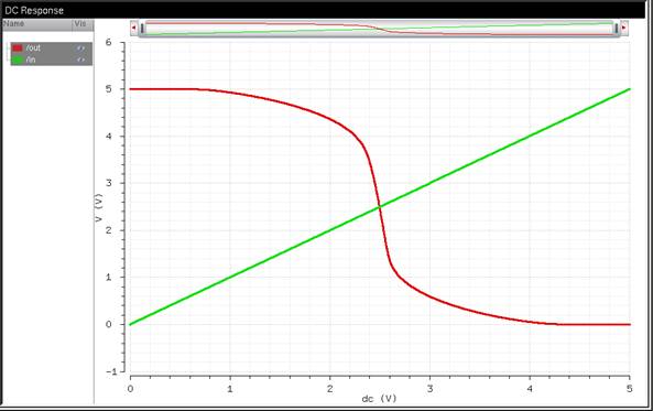
This concludes the Tutorial 3. I also did a simulation of my extracted
view and found it to be similar, if not the same, graph.
Lab
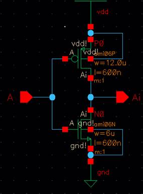
Draft schematics, layouts, and symbols for two inverters having sizes of
12u/6u and 48u/24u (M = 4).
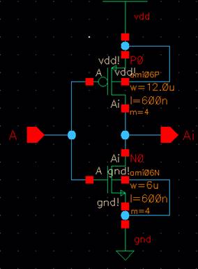
12u/6u schematic (left) and 48u/24u schematic (right)
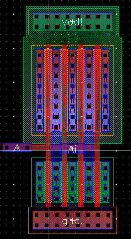
12u/6u layout (left) and 48u/24u layout (right)

12u/6u DRC Verified (left) and 48u/24u DRC Verified (right)


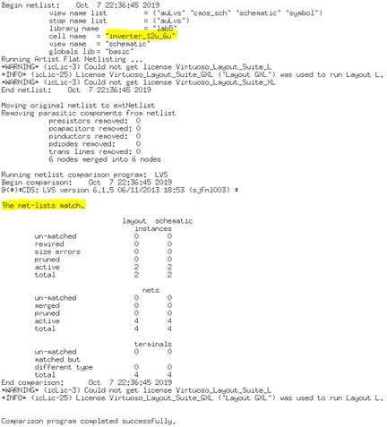
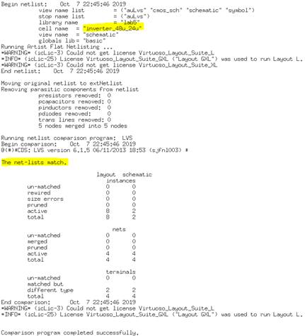
12u/6u LVS Verified (left) and 48u/24u LVS Verified (right)
12u/6u symbol (left) and 48u/24u symbol (right)
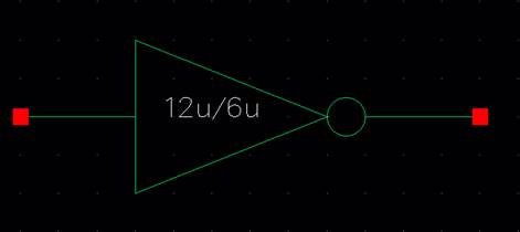
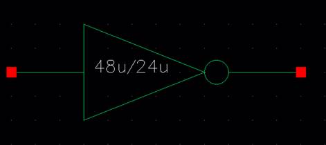
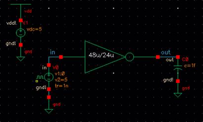
12u/6u sim schematic (left) and 48u/24u sim schematic (right)
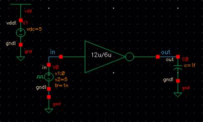
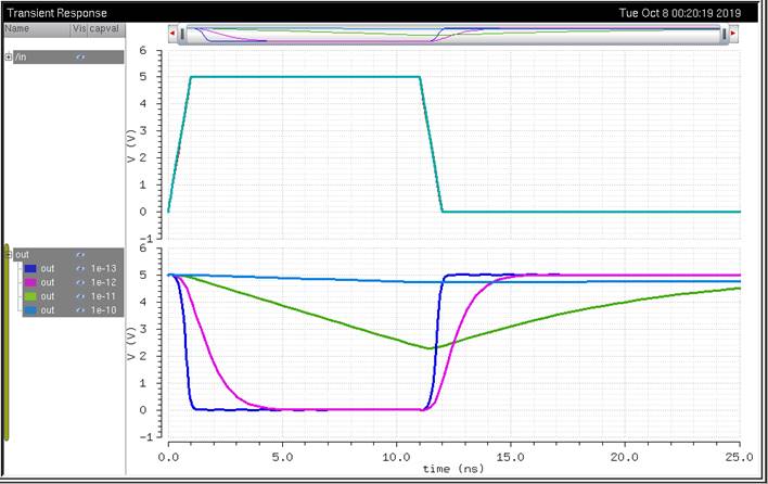
12u/6u spectre simulation (left)
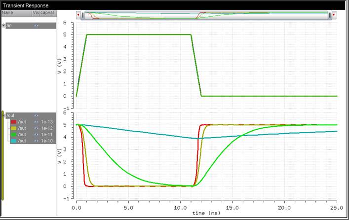
and 48u/24u spectre simulation (right)
‘capval’ represents the value of the capacitor:
1e-13 = 100 fF
1e-12 = 1 pF
1e-11 = 10 pF
1e-10 = 100 pF
12u/6u ultrasim (left) and 48u/24u ultrasim (right)
‘capval’ represents the value of the capacitor:
1e-13 = 100 fF
1e-12 = 1 pF
1e-11 = 10 pF
1e-10 = 100 pF
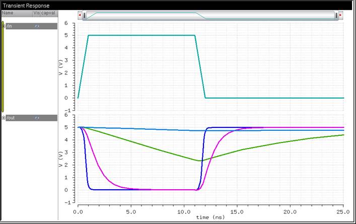
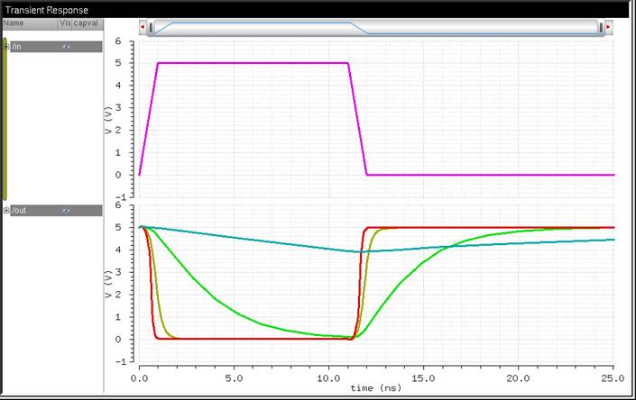
The UltraSim looks a bit cleaner and smoother.
But in terms of differences in approaches, I had to use a parametric set for
the spectre simulation, while I used a sweep using a
decade as the step mode with steps of 1 because UltraSim
wouldn’t allow me to use a parametric set.
I will be backing up my files on Google Drive in a .zip just as shown in
the previous labs.
