EE 421L –
Digital IC Design Lab - Lab 4
Authored by Chris Barr
Email: barrc1@unlv.nevada.edu
09/25/19
Lab
Description:
This lab pertains to the IV characteristics and layout of NMOS and PMOS
devices in ON's C5 process.
Prelab
I backed up my files of the previous lab through Google Drive.
Otherwise, this prelab pertains to the completion of Tutorial 2. There we
will go through the layout and simulation of the IV curves of PMOS and NMOS
devices.
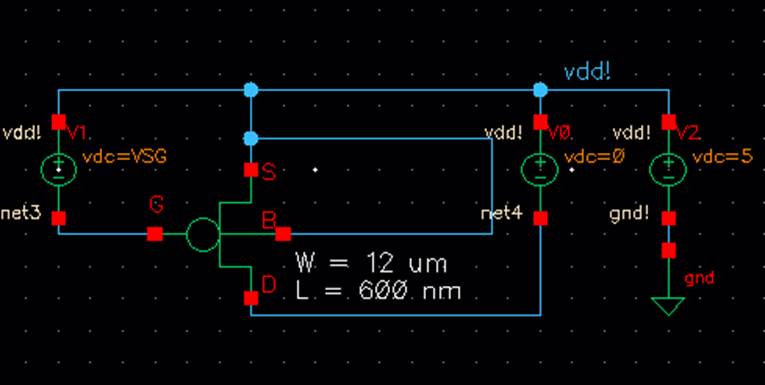
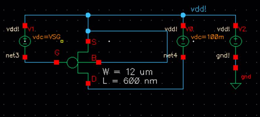
First, we’ll start by creating the schematic of the NMOS. It will include
the Source (S), Drain (D), Gate (G), and Body (!gnd)
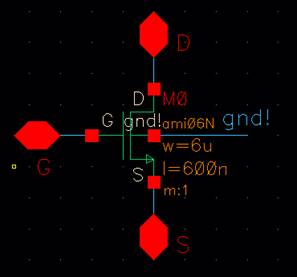
Fig. 1
Then, we’ll make a symbol that matches the schematic for that. Alongside
the symbol, we’ll place a small bit of text (SHIFT + N) that describes the
width and length of the transistor.
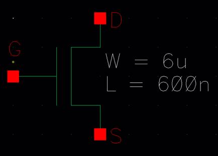
Fig. 2
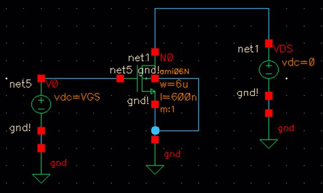
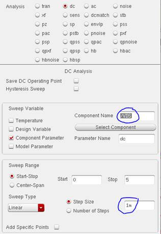
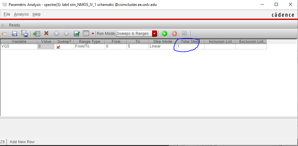
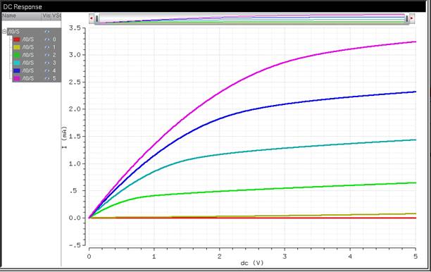
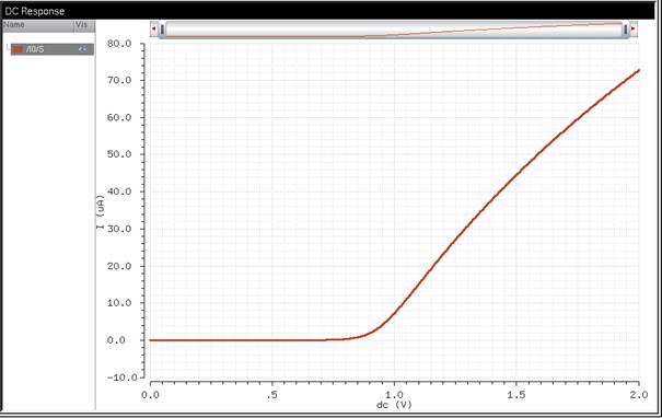
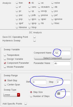
Using that same symbol, we’ll test it in a simulation to match this
schematic. This schematic will perform a linear step-up voltage of 1V going
from 0 to 5V.
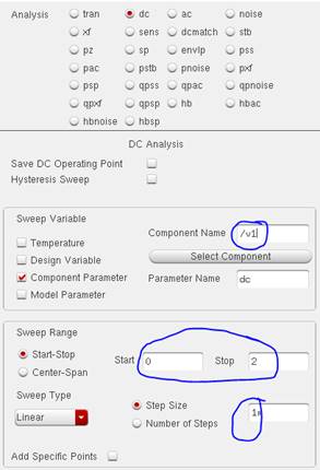
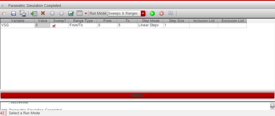
Following the instructions to set-up the Parametric Analysis view, we should
obtain an IV curve similar to the one down below.
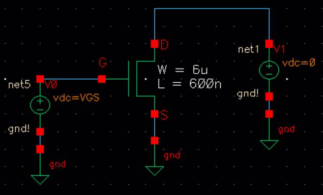
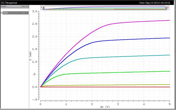
Fig. 3
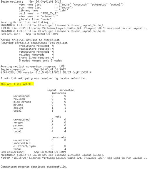
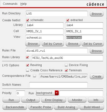
Now, we’ll move on to the layout view of the NMOS transistor. Once completed,
we’ll do an extraction and LVS it to the original schematic (Fig. 2).
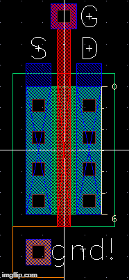
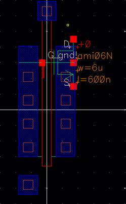
Fig. 4
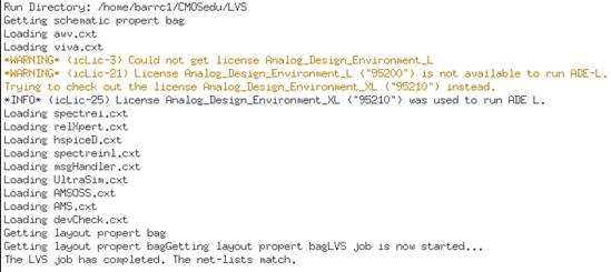
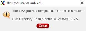
Fig. 5
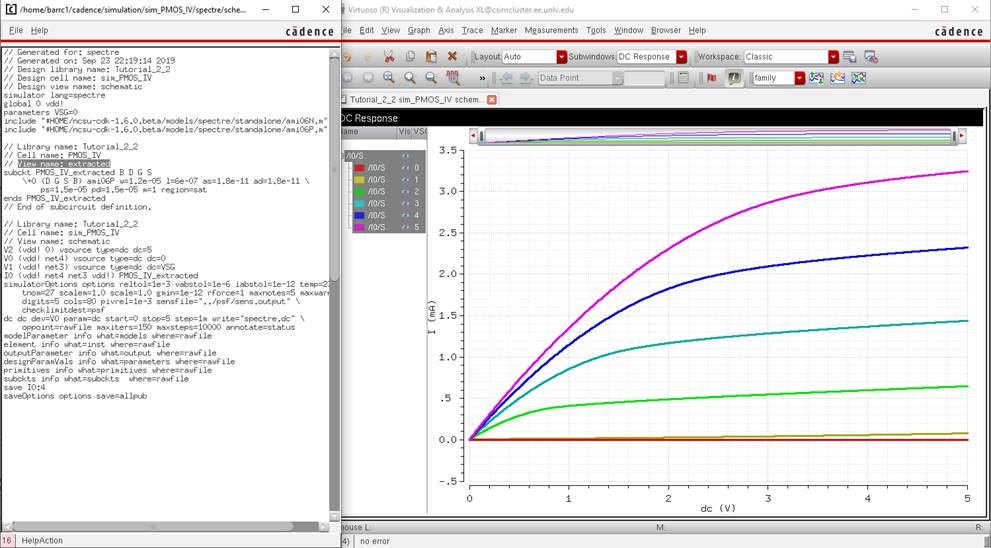
We’ll confirm that this works through simulation by making sure we use
the “extracted” to check the extracted view.
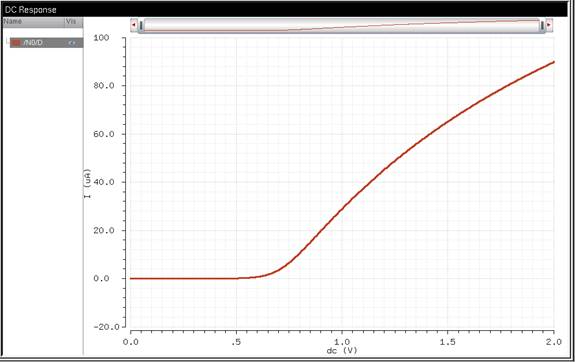
We can see that we get the same results, which is good.
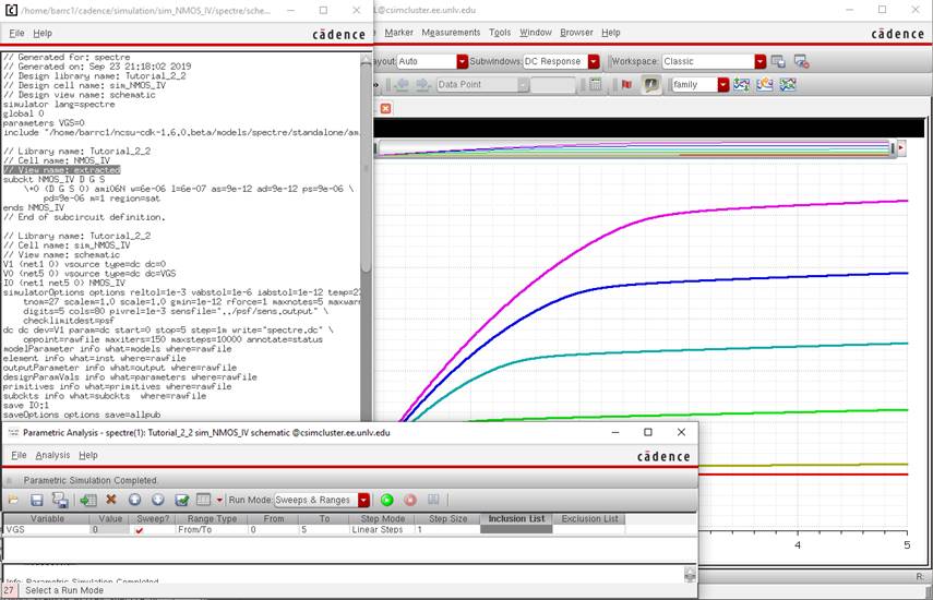
Fig. 6
We’ll repeat this process using a PMOS instead.
First the schematic, then the symbol, followed by the layout, and then
the extracted
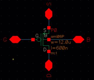
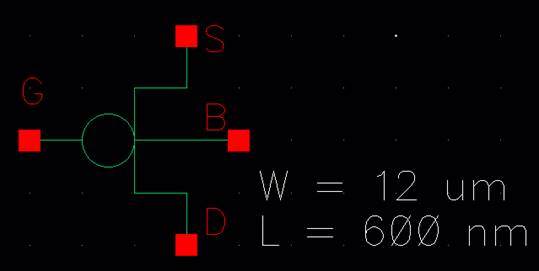
Fig. 7
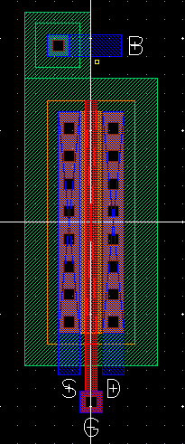
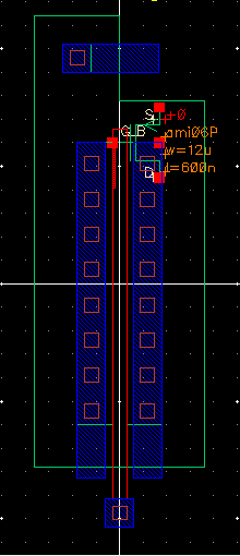
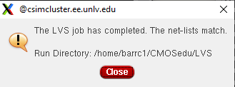
Fig. 8
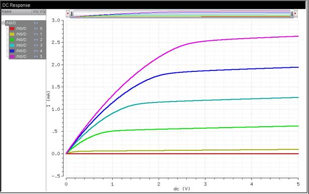
Now, we test it with a schematic shown down below.
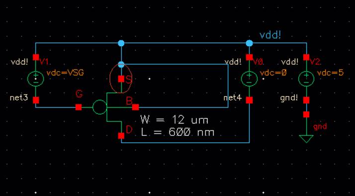
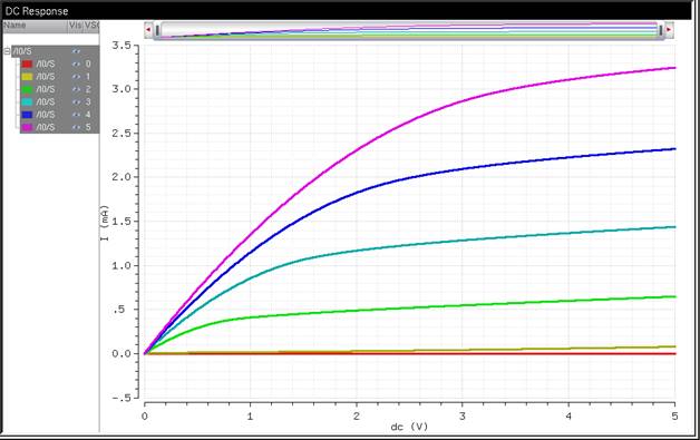
Fig. 9
And finally, we check it with the extracted view. And we received the
same result. This ends the prelab.
Lab
I’ll be generating 4 different schematics with their 4 simulations below.
Each pertaining to its own specifications.
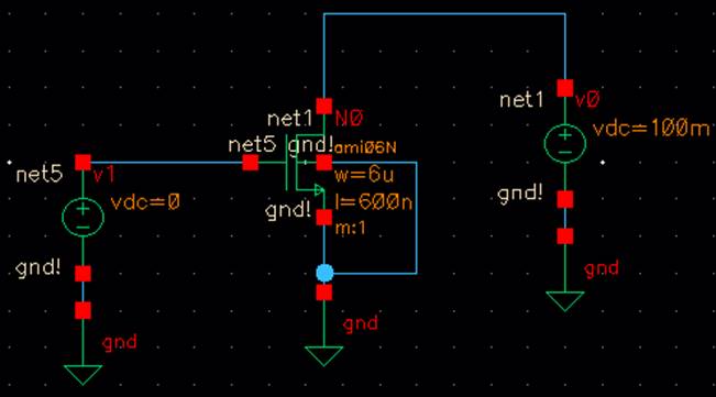
1.) A schematic for simulating ID v. VDS of an NMOS device for VGS
varying from 0 to 5 V in 1 V steps while VDS varies from 0 to 5 V in 1 mV
steps. Use a 6u/600n width-to-length ratio.
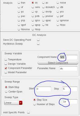
You can see that I use a 6u/600n ratio beside the NMOS in the schematic.
You can also see that I follow up to make sure that VDS goes up 1m step size,
and that the VGS is 1V steps.
2.) A schematic for simulating ID v. VGS of an NMOS device for VDS = 100
mV where VGS varies from 0 to 2 V in 1 mV steps. Again
use a 6u/600n width-to-length ratio.
Here, you can see that I continued to use the 6u/600n ratio NMOS. I made
VDS a static value of 100mV, while in the DC sweep I
made VGS start at 0 and stop at 2V with 1m steps just as asked.
Note: I will be using a PMOS symbol with the 12u/600n ratio shown in Fig.
7 during the prelab.
3.) A schematic for simulating ID v. VSD (note
VSD not VDS) of a PMOS device for VSG (not VGS) varying from 0 to 5 V in 1 V
steps while VSD varies from 0 to 5 V in 1 mV steps. Use a 12u/600n
width-to-length ratio.
Here, you can see the 12u/600n PMOS. I used a 0 to 5V VSD in 1 mV steps,
and 0 to 5V VSG in 1V steps.
4.) A schematic for simulating ID v. VSG of a PMOS device for VSD = 100
mV where VSG varies from 0 to 2 V in 1 mV steps. Again, use a 12u/600n
width-to-length ratio.
Here, you can see that I continued to use the 12u/600n ratio PMOS. I made
VSD a static value of 100mV, while in the DC sweep I
made VSG start at 0 and stop at 2V with 1m steps just as asked.
NMOS Layout
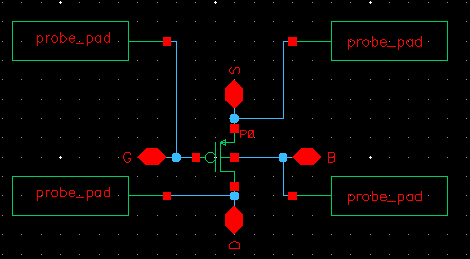
Lay out a 6u/0.6u NMOS device and connect all 4 MOSFET terminals to probe
pads (which can be considerably smaller than bond pads [see MOSIS design rules]
and directly adjacent to the MOSFET (so the layout is relative
small).
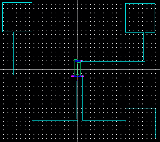
I’ll first attach the NMOS layout, and apply
m2_m1 and m3_m2 via’s.
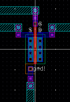
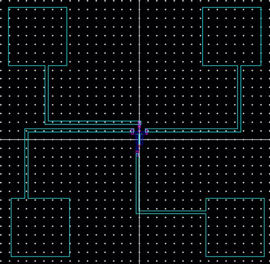
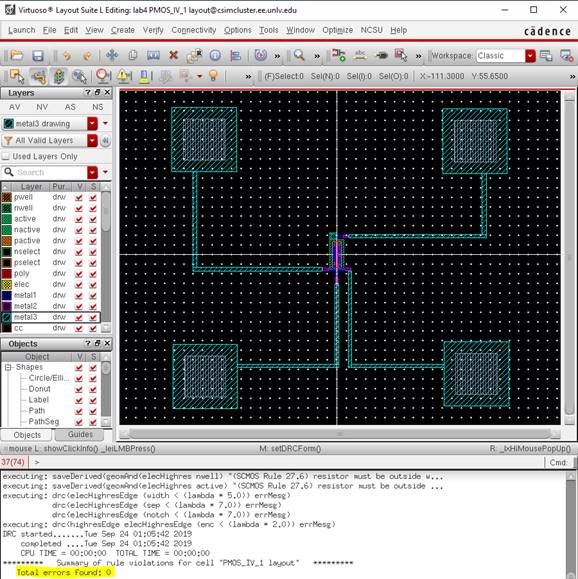
Then, I’ll be able to stretch out the metal3 to the pads. This will
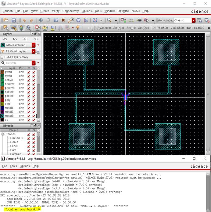
complete the layout, and I can verify it with DRC.
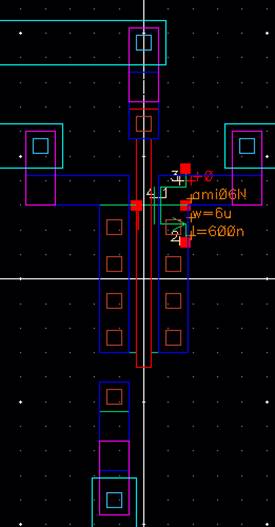
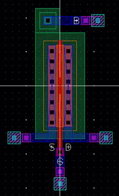
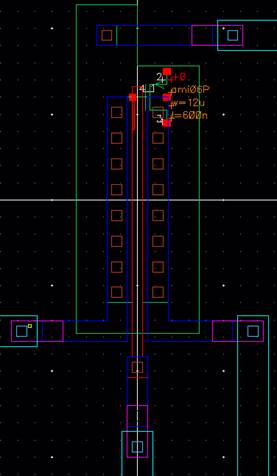
This is the extracted view with a close-up on the transistor.
Now, I’ll make the schematic to verify if my extracted layout works.
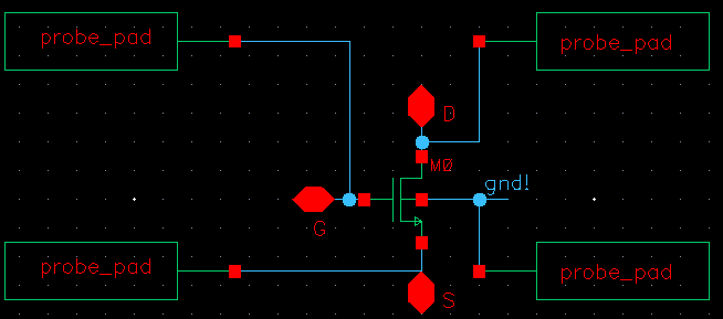
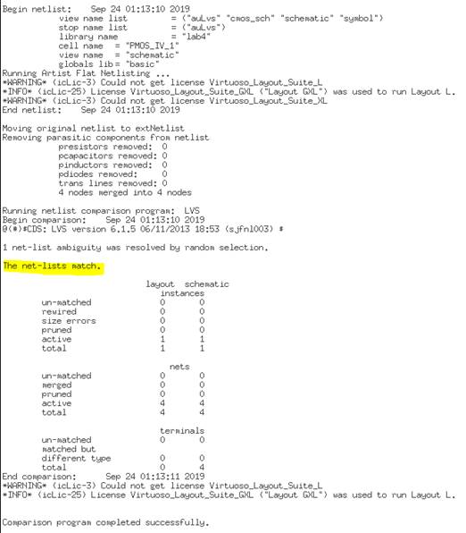
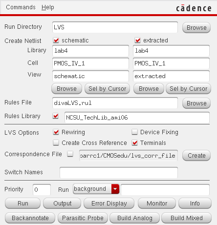
Finally, the LVS check.
NMOS Layout
Lay out a 12u/0.6u PMOS device and connect all 4 MOSFET terminals to
probe pads.
Again, I’ll start by laying out the PMOS including the via’s.
Then, I’ll be able to stretch out the metal3 to the pads. This will
complete the layout, and I can verify it with DRC.
This is the extracted view with a close-up on the transistor.
Now, I’ll make the schematic to verify if my extracted layout works.
Finally, the LVS check.
I will be backing up my lab files using Google Drive
This folder will be placed
into my Google Drives “backup_labs” folder followed by another folder
corresponding to that particular lab, like so…