EE 421L –
Digital IC Design Lab - Lab 3
Authored by Chris Barr
Email: barrc1@unlv.nevada.edu
09/18/19
Zipped Lab3
folder:
Note: My schematic, layout, and extracted design are within the cell-view
of “My_10-bit_DAC”
Lab
Description:
This lab will be going over the layout portion of the 10-bit DAC. We’ll
create a layout that resembles the 10-bit DAC we created in the last lab, and
then verify it with DRC and LVS.
Prelab
At the end of my previous lab (lab 2), I showed how I backed up my files,
like so
Continuation
of Tutorial 1
We start by creating a voltage divider schematic using 10k ohm resistors.
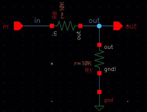
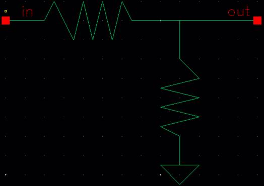
Using those input and output pins, we create our symbol. We redrew the
schematic using lines to resemble the voltage divider.
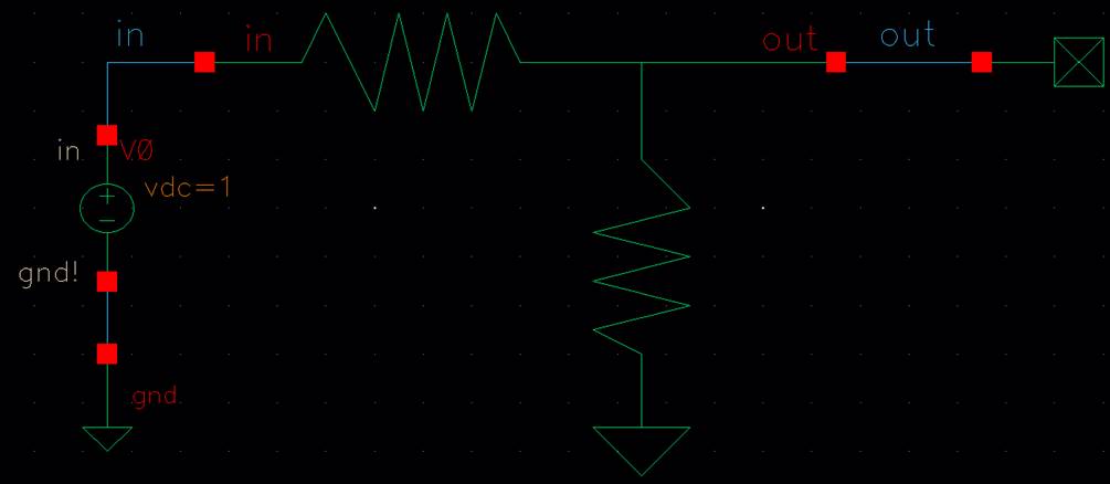
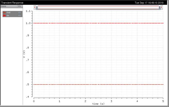
Afterwards, we place the symbol into a schematic and simulate it to
verify if it’s functional. We’ll be using a 1V input with the expectations of a
0.5V output.
Now that we know our schematic works with our symbol, we can continue to
the layout view. But first, we need to recreate the 10k ohm resistor as an
n-well resistor in layout.
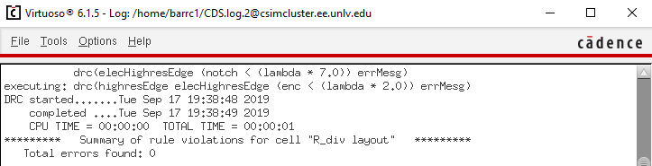
Once we create the layout for the 10k ohm resistor, we do a DRC verification to
see if we’re following the rules for design.

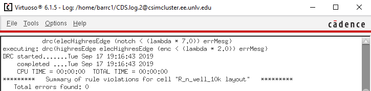
When the DRC verification approves the measurements. We can proceed to
extract the layout. If the extracted layout is close enough to the 10k ohm
resistance, then we can continue to making the layout
identical to the original schematic.

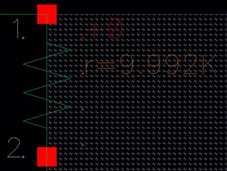
We can instantiate the 9.992k ohm resistor in the layout view so we can
recreate the original schematic. We’ll follow up with a DRC verification like
earlier.
Finally, we can extract the layout and LVS for verification. Verifying
using LVS is a way to determine if the layout is identical to the original
schematic so it can be chip design ready.
This end Tutorial 1 with a successful verification to the original
schematic.
Lab
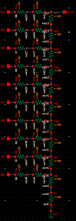
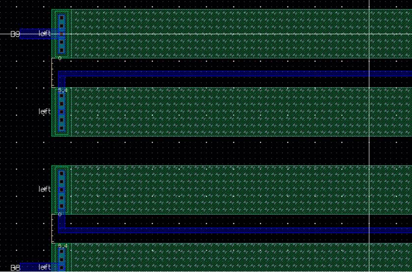
This lab we’ll recreate the 10-bit DAC on the layout view. Below is the
10-bit DAC I had created in the previous lab (lab 2). We’ll be using the same
10k ohm resistor created in the prelab to complete the layout.
Q1.) Discuss, in your lab
report, how to select the width and length of the resistor by referencing the
process information from MOSIS
·
We can reference the process information from MOSIS through their website
on the pdf they provide here
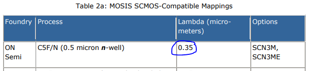
In this pdf, we can scroll down to Table 2a
where we can find the lambda value for our C5 process.
Scroll down further to Table 3a and we can
find the scalable CMOS (SCMOS) for the well’s width.
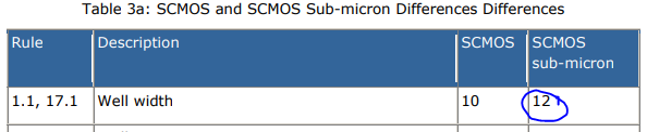
Using this information, we can take the
lambda value for the C5 process, and multiply by 12 to obtain the minimum width
value we can have for our resistor.
12* lambda = 3.6 um.
From there, we know that the C5 process uses an 855 ohms/square, as shown below
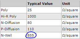
Assuming we want a 10k ohm resistance, we
can calculate it like so
L/W = 10k ohms / (855 ohms/square)
= 11.6959 squares
ð L = 11.6959*W
ð L = 11.6959(3.6 um)
ð L = 42.1 um
Using the minimum width value
we can possibly use, we can find that the minimum length we can use is 42.1 um.
And that’s how we can select our width and length referencing MOSIS.
Q2.) Discuss, in your lab
report, how the width and length of the resistor are measured
·
We can measure the width and length of our resistor by simply following
the same process we used earlier
If you know the sheet resistance of the
process you choose (in our case, the C5 process), you just need to choose the
value of resistance you want your resistor to have. Assuming the 10k ohms
resistance, like earlier, you can find the width to length ratio.
L/W = 11.6959 squares
L = 11.6959*W
L = 11.6959, W = 1
This is a 11.6959:1 ration where L:W. So long as the width is divisible by 0.15 um, the width
should be acceptable. And then round up to the nearest divisible 0.15 um of the
length.
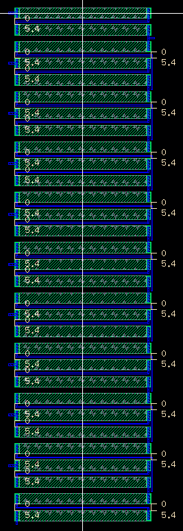
Continuing the lab, first we’ll be instantiating the 9.996k ohm
resistance created in the prelab. We’ll make sure that the resistors are within
5.4 um apart.
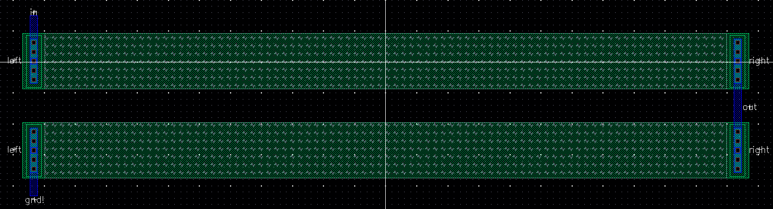
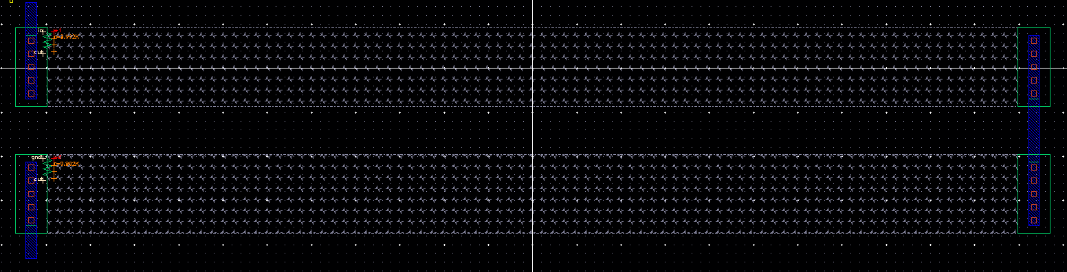
Afterwards, we can continue to lay out the rest of the resistors. And
wire them together with metal1.
At the end, this is what our layout and extracted layout will look like:
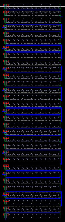
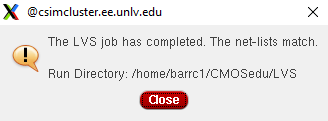
We’ll run the LVS with the 10-bit DAC schematic.
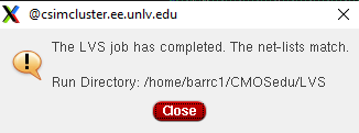
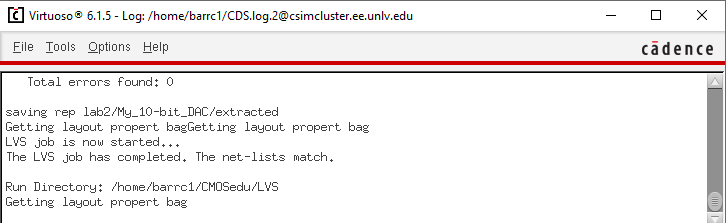
The netlists match, this means the layout is chip design ready.
My lab 3 files will be backed up using the same method shown in the
prelab; through google drive.