EE 421L –
Digital IC Design Lab - Lab 2
Authored by Chris Barr
Email: barrc1@unlv.nevada.edu
09/04/19
Lab
Description:
This lab will be covering how to design a 10-bit digital-to-analog
converter (DAC).
Prelab
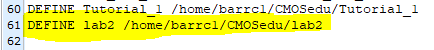
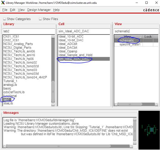
We download lab2.zip and unzip the files into a new library we created
called “lab2”
The library is defined in our cds.lib
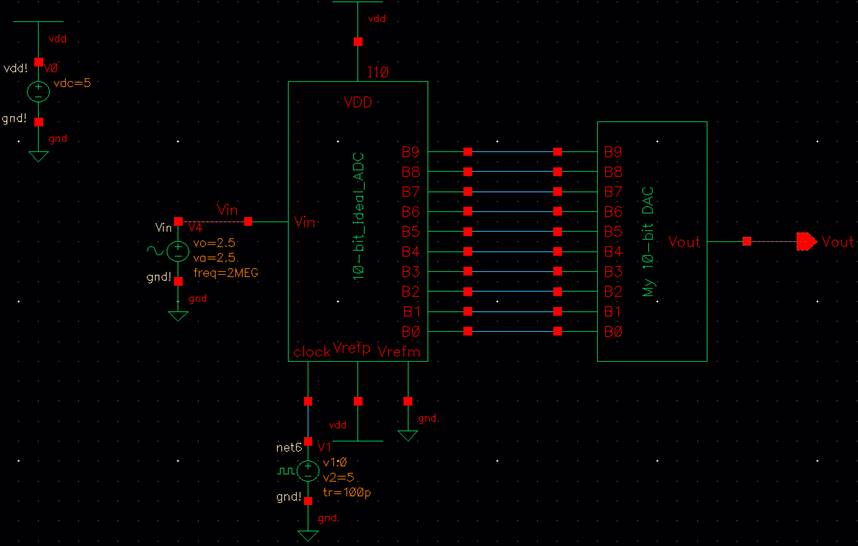
Afterwards, we’ll be able to see the “lab2” library with the cell view “sim_Ideal_ADC_DAC”
Left-click that and go into the schematic
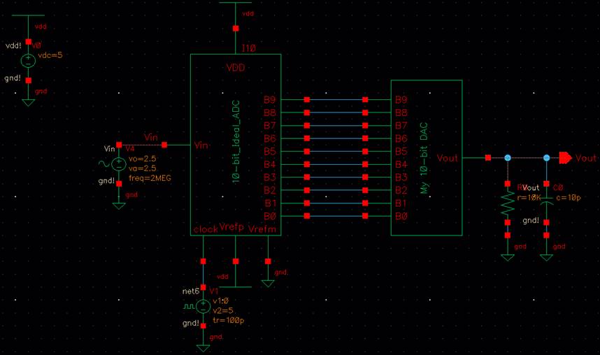
This is the 10-bit ideal ADC & DAC schematic we’ll be simulating
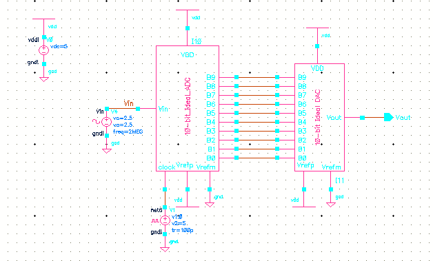
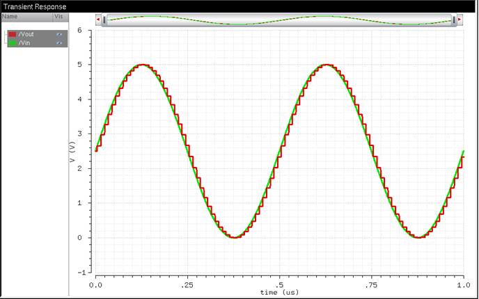
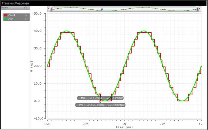
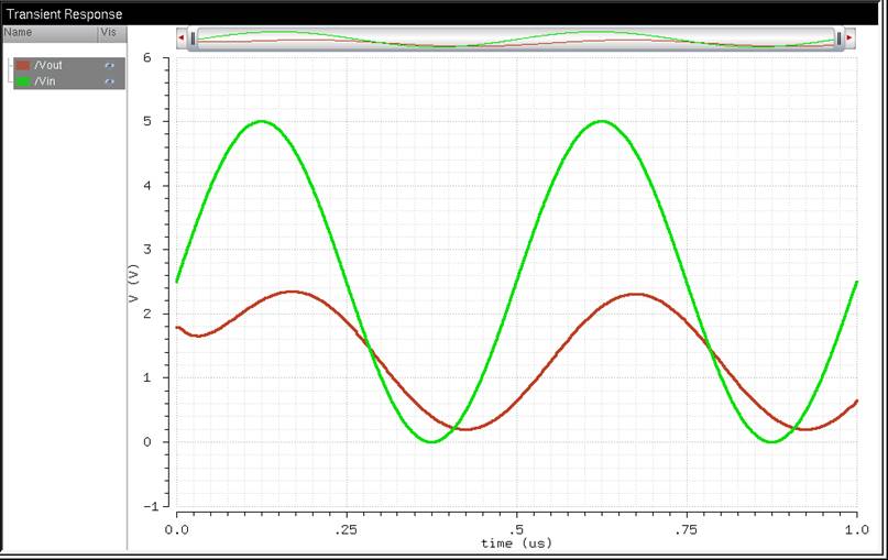
This is the simulation results we get from loading the state it came with:
Providing, and discussing, simulation results from my own example to
illustrate my understanding of the ADC and DAC
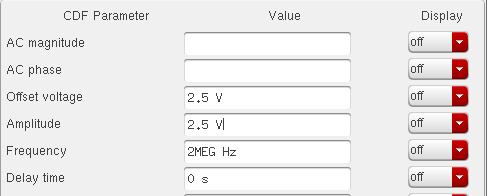
Here’s the original values of Vin for the Offset and Amplitude values
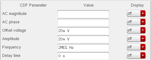
Here are the new values of Vin for creating my own illustration
When we simulate this, we get this result:
By doing this, we can notice the change in number of steps created. It
takes less steps to get to a 40 Vpp than a 5 Vpp.
This shows that by changing the Vin’s value does have an effect on B[9:0].
Here’s my understanding on how to determine the least significant bit
(LSB):
Using the Least Significant Bit (LSB) equation:
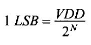
Where,
N = number of bits = B[9:0] = 10 bits
VDD = Reference Voltage = 5 V
1 LSB = ![]() =
= ![]() = 4.88 mV
= 4.88 mV
The
denominator gives you the max value a 10-bit ADC can obtain. By dividing it
with the 5V reference voltage, we can then find the 1 LSB value, which in our
case is 4.88 mV.
The calculation result compares to the simulation when going from 0V up to the
next step which is 4.88mV. The next step afterwards is just another addition of
4.88mV.
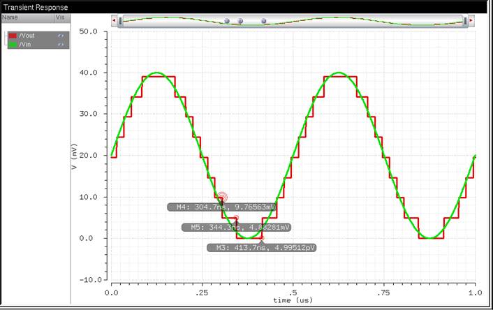
For
further analysis, we can take a look at this other illustration I created to
test the validity of the equation:
Again,
using the equation:
1 LSB = ![]() =
= ![]() = 3.906 mV
= 3.906 mV
You can
see that going from 0V to the next step upwards gives 3.90625mV from the simulation.
So, whether changing Vin, or the Vref, can change the
outcome of our results.
Lab
In this lab, we will be using n-well resistors to recreate the 10-bit
DAC, similarly shown in this figure:
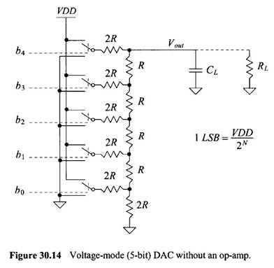
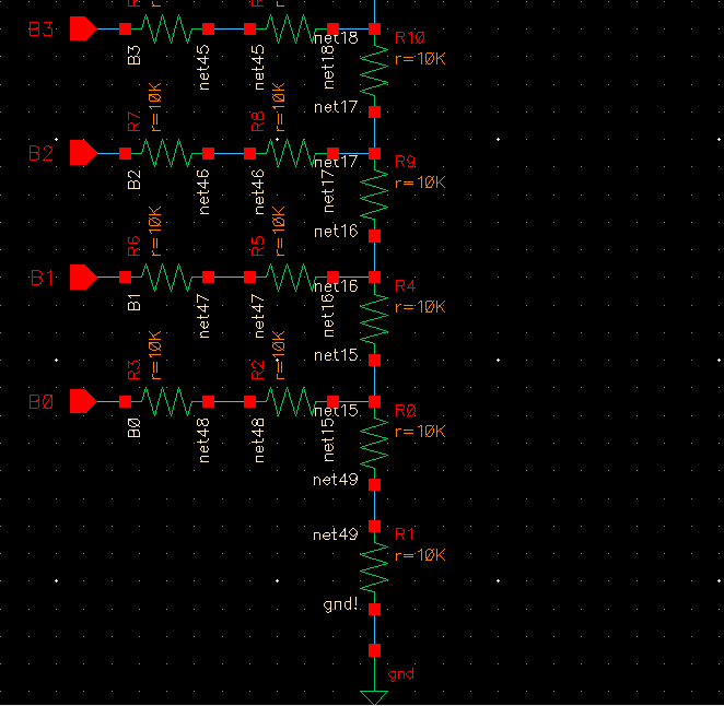 Creating it on
Cadence we used 10k ohm resistors as our R, and used two 10k ohm resistors in
series for the 2R.
Creating it on
Cadence we used 10k ohm resistors as our R, and used two 10k ohm resistors in
series for the 2R.
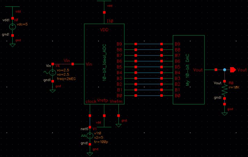
This is my full schematic design for the 10-bit DAC.
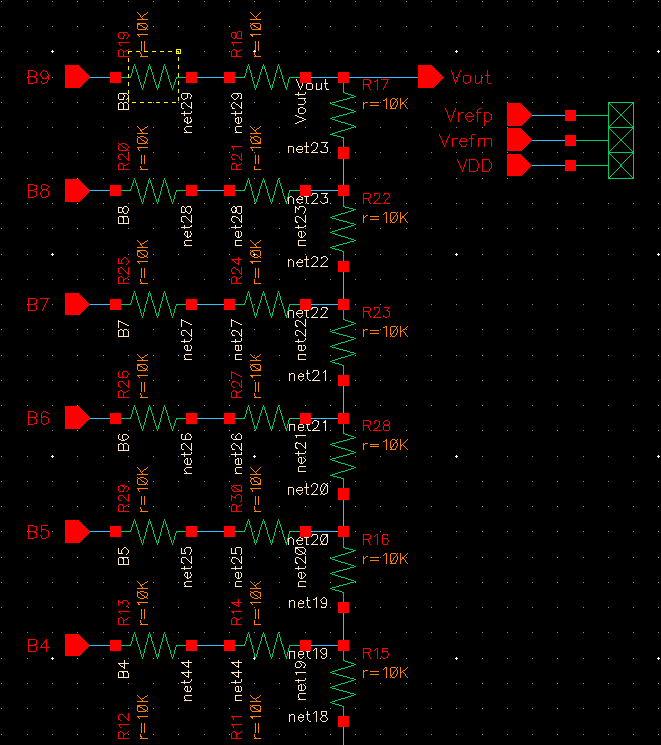
Note: I did get rid of the ‘Vrefp’, ‘Vrefm’, and the ‘VDD’ wires by deleting them. Because of
this, my new symbol now appears like so:
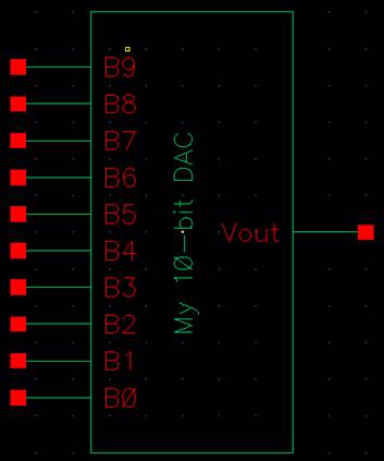
A symbol can be created by going to the original schematic and going to
the toolbar above
Create > Cellview > From Cellview
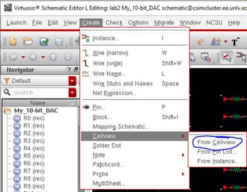
Nothing needs to be changed, the user can then press ‘OK’.
If we would like to determine the output resistance of the DAC, we would
want to refer to these set of equations down below
Parallel:
2R||2R = 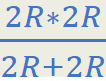 = R
= R
Series:
R + R = 2R
LOAD 10pF TO DAC
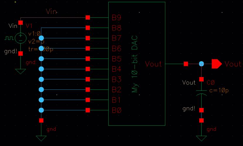
Using only
my 10-bit DAC, I’ll be putting a 10pF load located at Vout
while grounding all the input pins but B9. The input voltage of B9 will
receive a 5V pulse.
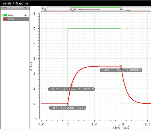
We can predict that the capacitor will charge to 1.25V (half of the 2.5 Vpeak) by calculating:
0.7τ = 0.7RC =
0.7(10k)(10p) = 70 ns
This
implies that capacitor will charge to 1.25V by 70 ns
Verifying if My DAC works
properly
I copied
the original “sim_ideal_ADC_DAC” schematic to another
cell to test my DAC. Then, I replaced the ideal DAC with my own.
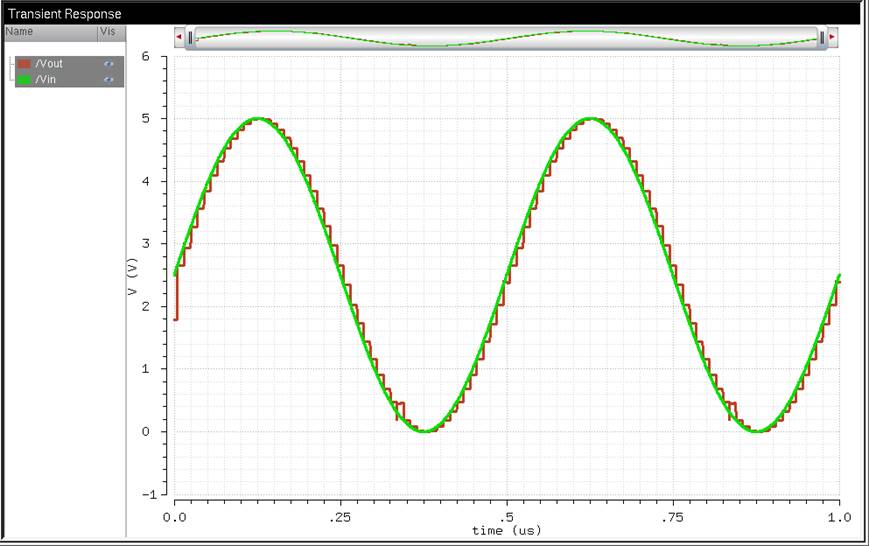
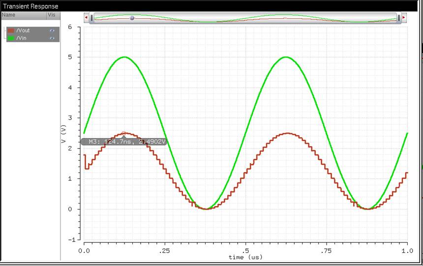
Using a 2.5Vpp input voltage with a 2.5V voltage offset (the same as
the original design setup), we’ll notice it’s nearly, if not exactly, the same
results in the simulation.
Simulations loading an
R, C, and R/C
Resistor as load
I drove a
10k ohm resistor. This cut the Vout in half and only
peaks at 2.5V.
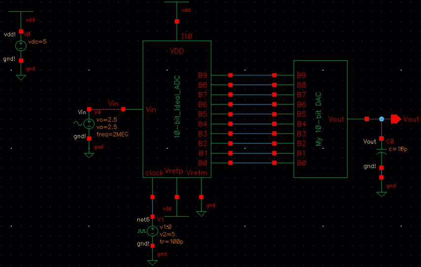
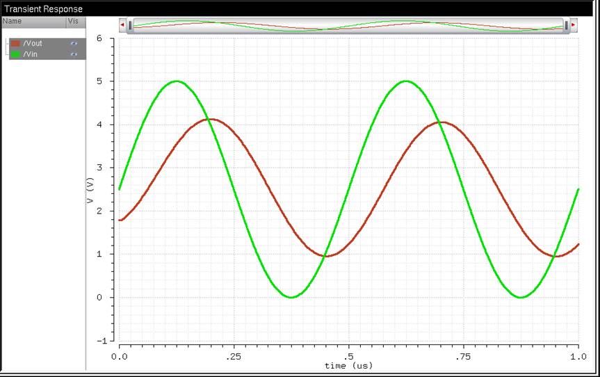
Capacitor as load
I drove a
10pF capacitor. Because the capacitor has a delay to charge Vout
fully, it will offset it by the 70ns we calculated earlier. Also, because of
this delay, it doesn’t charge all the way up to 5V or discharge down to 0V.
Resistor and Capacitor as
load
I drove both the 10k ohm and 10pF
capacitor.
Q.) Explain what happens
if the DAC drives a 10k load?
When you drive a 10k ohm load, like what was shown earlier. The Vout will specifically cut in half because it’s being
voltage divided by the other 10k ohm resistors inside the DAC.
Q.) Discuss what happens
if the resistance of the switches isn't small compared to R.
If the resistance of the switch
isn’t small in comparison to R, like in figure 30.14 above, then we would have
to recalculate the resistances within the DAC because this would have a more
than noticeable effect on the output voltage. To ensure that the circuit would
still work, we would have to recalculate the resistance to match the load
resistance.
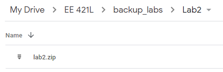
Files are
backed up as shown below: