Serial to Parallel Converter Project - ECE 421L
Authored
by Esteban Tuquero,
November 13, 2018
Description
Design
a serial-to-parallel converter that takes serial input data and an
associated clock signal and generates an 8-bit output (parallel) word
and clock.
Schematics
Transmission Gate (TG)
Before designing the converter or even the D flip-flop it is necessary to design the schematics for the transmission gate.
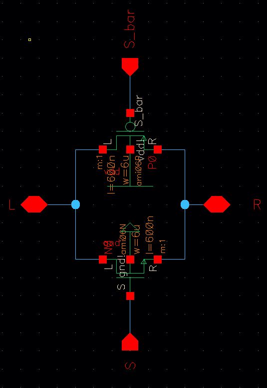 | 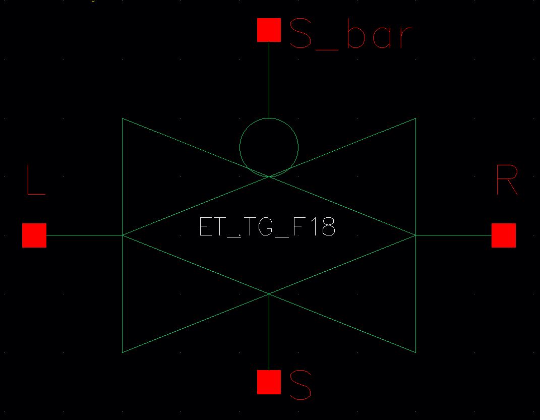 |
| Schematic for TG | Symbol for TG |
Notice that the left (L) and right (R) terminal pins are input/output, this is because the nodes are interchangeable.
D flip-flop
In order to design the converter, a D flip-flop is necessary because of it's ability to store inputs.
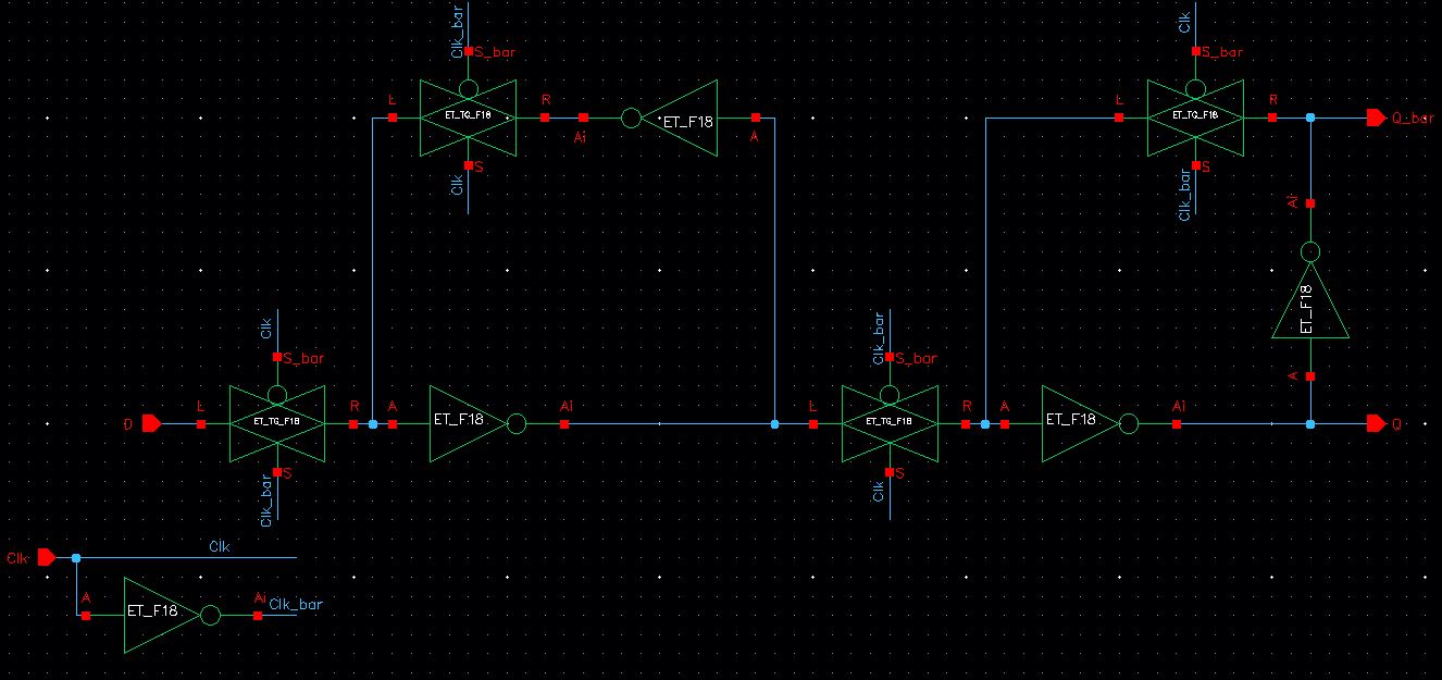 |
| Schematic of D flip-flop |
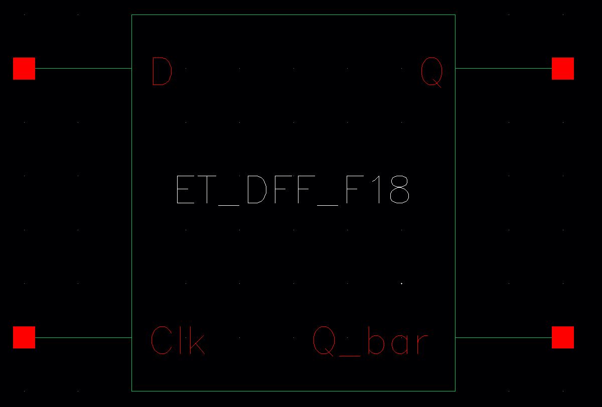 |
| Symbol of D flip-flop |
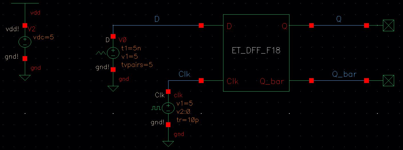 |
| Schematic for simulating D flip-flop |
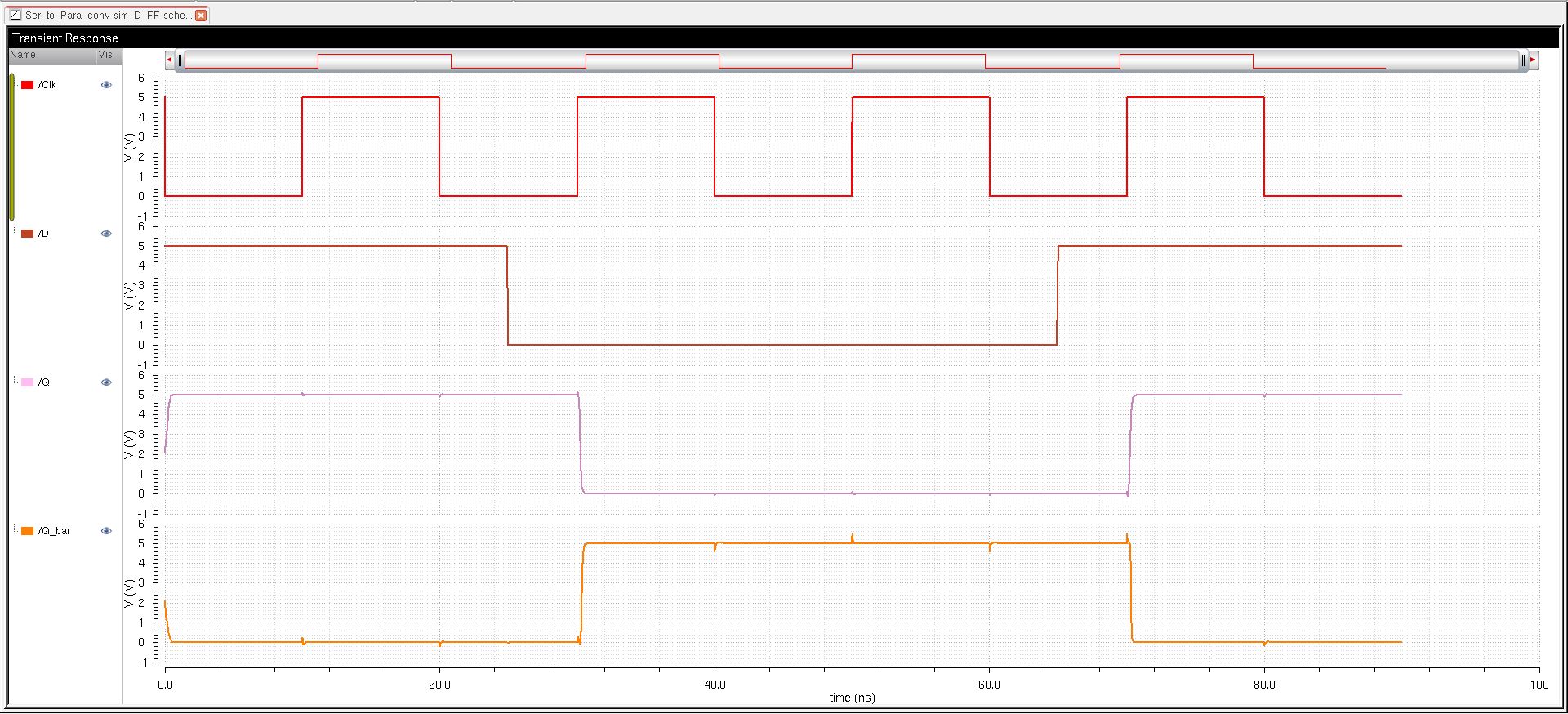 |
| Simulation of D flip-flop |
When
simulating the the D flip-flop, I used the signal input (D) of 1001.
The D flip-flop is able to output the signal on each rising edge of the
clock, which is what we desire. However, there are small glitches in
the output at every edge of the clock. This is probably due to the
differences in rise and fall time.
Serial-to-Parallel Converter
The
most significant bit (MSB) of the of the 8-bit input is first put into
the first D flip-flop D<0>. At each rising edge clock-cycle the
next significant bit gets stored until the MSB is stored into
D<7>. Finally as the delayed clock (clock_out) is on the rising
edge the converter will output the 8-bit byte.
 |
| Schematics for Serial-to-Parallel Converter |

|
| Serial-to-Parallel Converter Symbol |
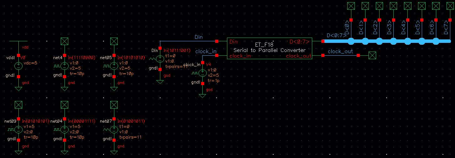 |
| Schematics for simulating Serial-to-Parallel Converter |
For
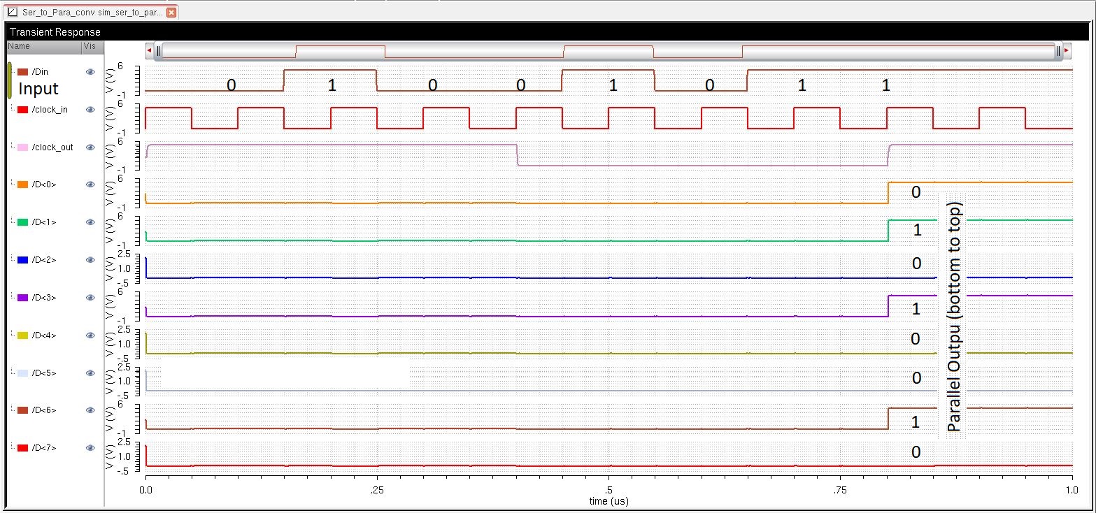
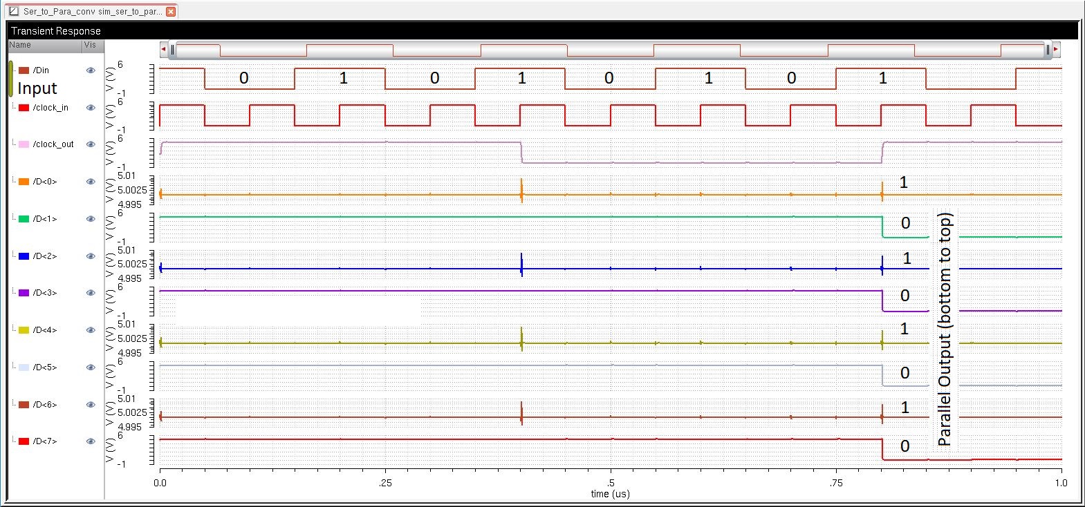
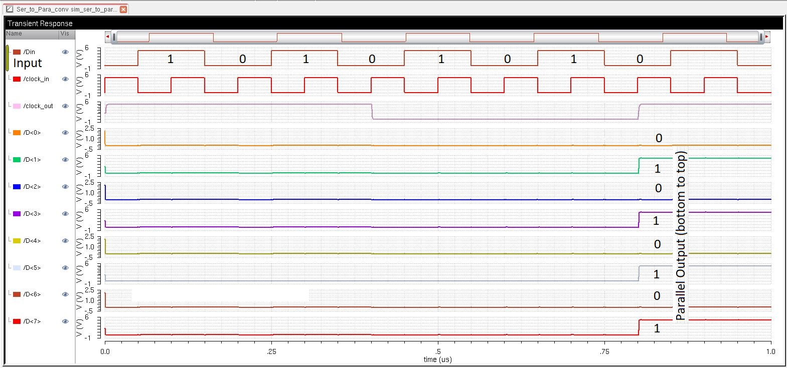
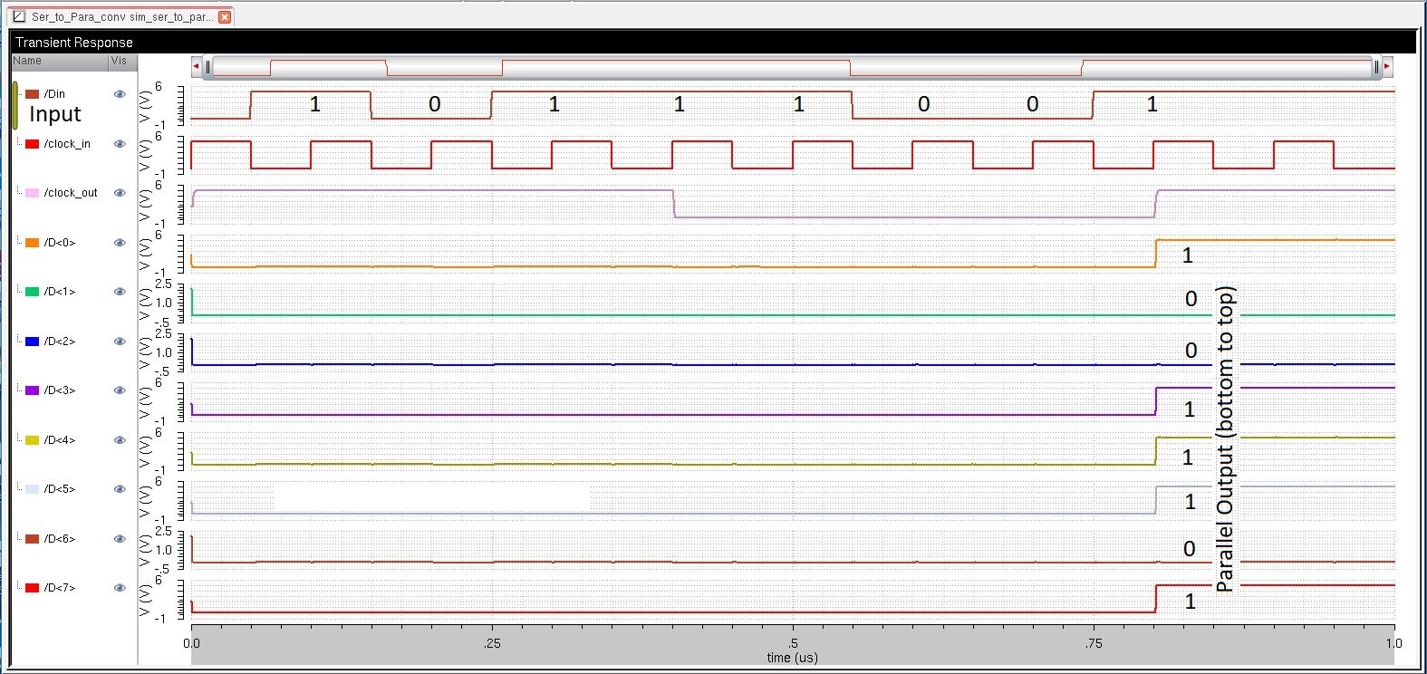
testing the converter I used 6 different 8-bit combinations (00001111,
01001011, 01010101, 10101010, 10111001, and 11110000). The reasons that
I chose these numbers were to see if there would be any problems with
taking the complement of a combinations and seeing how the converter
would react as the clock_out switched from high to low propogation.
 |
| Simulation for 00001111 |
 |
| Simulation for 01001011 |
 |
| Simulation for 01010101 |
 |
| Simulation for 10101010 |
 |
| Simulation for 10111001 |
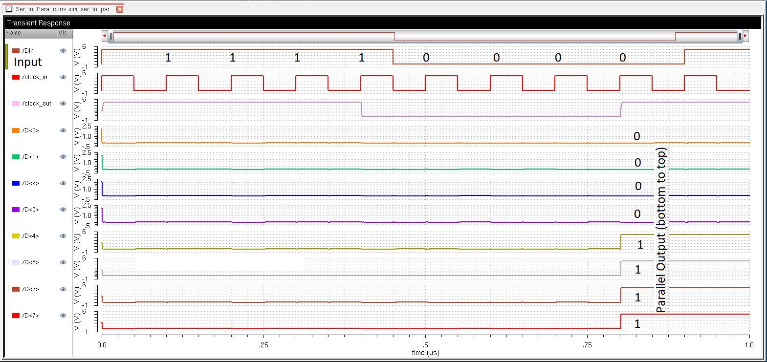 |
| Simulation for 11110000 |
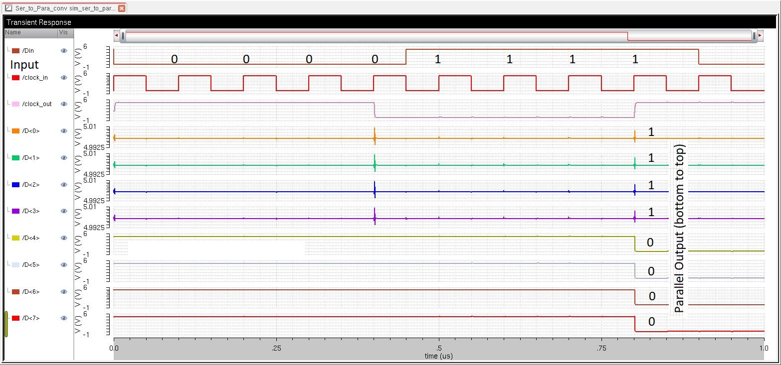
Notice
that the input puts in the MSB into D<7> because it is the last
register in the converter. This is because the MSB should be the first
input and the LSB should be the last. For the input 10111001 the
corresponding registers are D<7>, D<6>, D<5>, ...,
D<0> There are also still some small spikes on all of the edges
of the clock (rising and falling). This is most notable in the
simulations for 01010101 and 00001111 with the most significant spike
at the point where clock_out switches from high to low. These spikes
are relatively small (1mV to 10mV), so they can be ignored.
Layouts
Transmission Gate
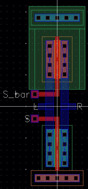 |  |
| TG Layout | TG DRC |
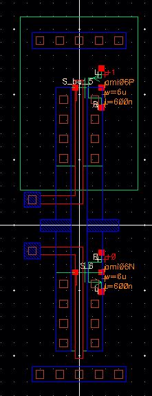 | 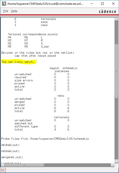 |
| TG Extracted View | TG LVS |
D flip-flop
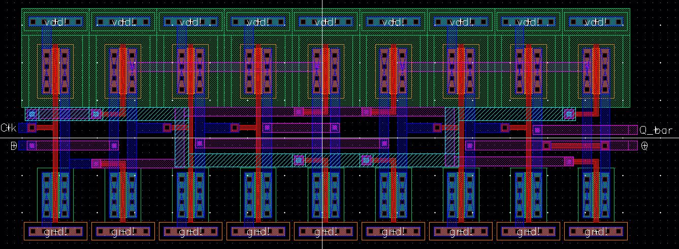 |
| D flip-flop Layout |
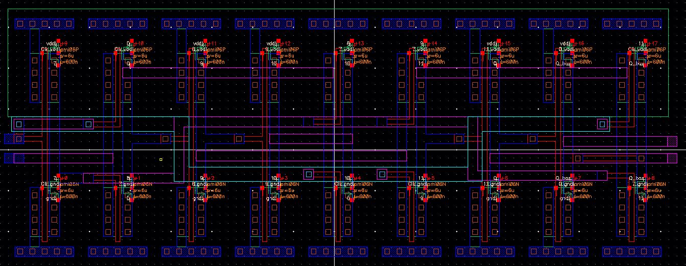 |
| D flip-flop Extracted View |
 | 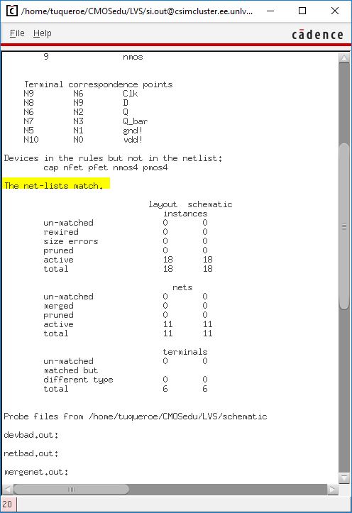 |
| D flip-flop DRC | D flip-flop LVS |
Serial-to-Parallel Converter
The following images are close ups of the inputs of the converter and some outputs of the converter.
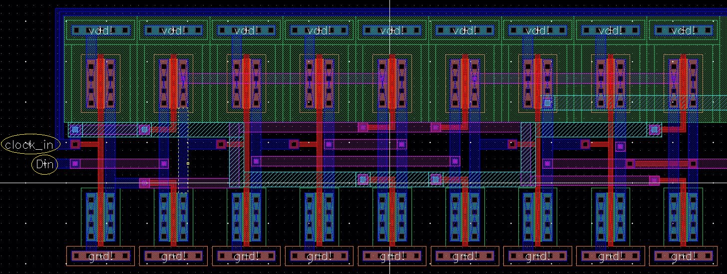 |
| Close Up of the Inputs clock_in and Din |
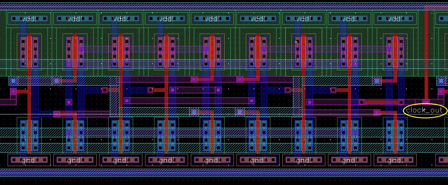 |
| Close Up of the Output clock_out |
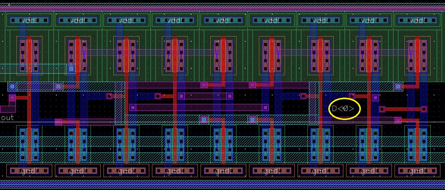 |
| Close Up of Output D<0> |
The following images show the whole layout of the converter with inputs and outputs highlighted.
Shift Registers
Reduced Clock
Hold Registers
 | 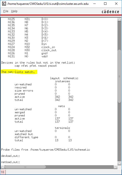 |
| Serial-to-Parallel Converter DRC | Serial-to-Parallel Converter LVS |
Files can be found here.
Return to my labs