 Project – EE 421L
Authored by: Daniel Senda
Email: sendad1@unlv.nevada.edu
Fall 2018
1st half due: 11-14-2018
2nd half due: 11-21-2018
1) 1st Half
of Project Description
-The first
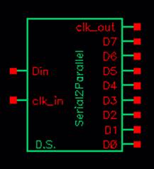
half of the project required the student to design an 8-bit serial-to-parallel
converter. The converter takes in 8 bits of data in a serial manner (at a speed
of 10Mbits/s), and then outputs the 8 bits in a parallel fashion. The converter
has two inputs, Din and clk_out, and nine outputs,
D7-D0 and clk_out.
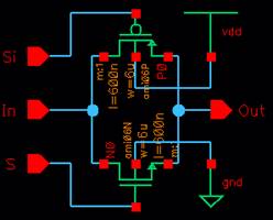
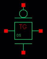
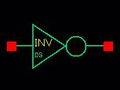
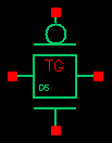
- One of the
initial building blocks of the converter is a transmission gate (TG) device.
The student created a schematic and symbol for the TG to be used in the design.
TG schematic: TG symbol:
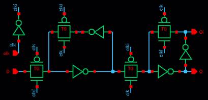
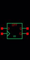
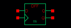
-After
creating the TG, the next fundamental element to create was an edge-triggered D
flip-flop. The D flip-flop is composed of TGs and inverters. The student
created the schematic and symbol for the D flip-flop as well. Then a simulation
was ran to insure the flip-flop worked correctly.
Edge-triggered D flip-flop schematic: Symbol:
D flip-flop simulation schematic: Simulation waveform results:

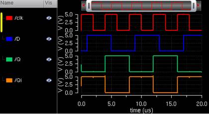
As can be seen, the output Q takes the value of input D at every rising edge of
the clock signal.
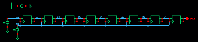
-Next, the
student created an 8-bit shift register from a string of edge-triggered D
flip-flops. The schematic was tested to show the register was shifting
correctly.
8-bit shift register schematic:
Simulation waveform results:
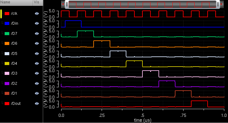
The simulation shows that the register is correctly shifting the high value of
Din down the register at every rising edge of the clock signal.
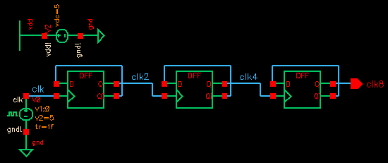
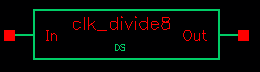
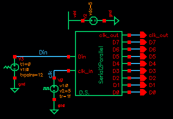
-A
serial-to-parallel converter consists of a shift register, a hold register, and
a clock divider. The clock divider value depends on the number of bits of the
converter. In the case of an 8-bit serial-to-parallel converter, the clock
needs to be divided by 8. The divided clock signal is used to control the hold
register. In order to divide the signal by 8, the student implemented 3
edge-triggered D flip-flops to create a schematic and symbol.
Clock divided by 8 schematic:
Simulation waveform results:
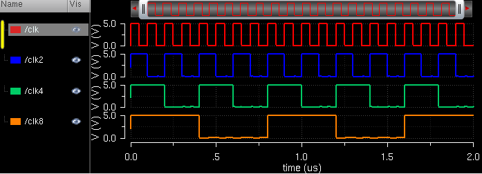
Each flip flop
divides the clock signal by 2. After the third flip flop, output clk8 is 8
times slower.
Clock divided by 8 Symbol:
- Lastly, the
student connected these parts together to create a schematic for the 8-bit
serial-to-parallel converter. In addition, a symbol was created and it was used
to simulate the operation of the converter.
8-bit serial-to-parallel schematic:
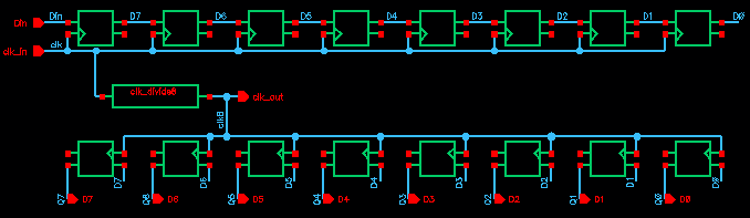
Converter symbol: Converter simulation
schematic:
1 0 0 1 0 0 1 1 1
1 0 0
1 0 0
1
1st Simulation waveform results:
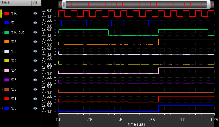
The first simulation shows the binary number 10010011 (147) being fed into the
converter at 10Mbits/s. The number is then outputted on the output lines D7-D0,
with D7 being the most significant bit, after clk_out
(clock divided by 8) goes high.
0 1 0 1 0 1 1 1 1
1 1 0
1 0 1
0
2nd Simulation waveform results:
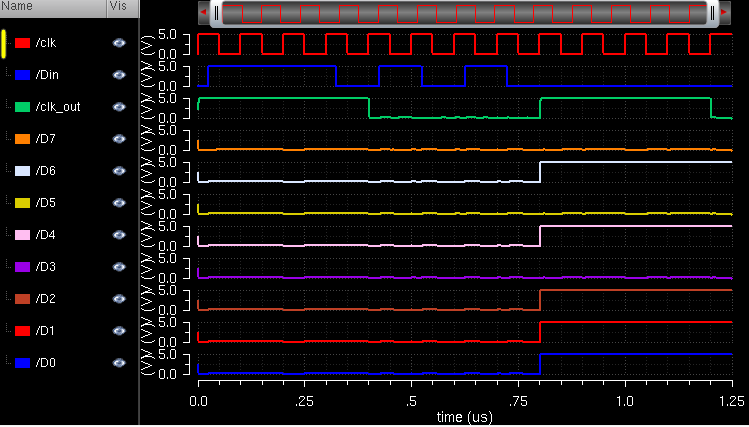
The second simulation shows the binary number 01010111 (87) being fed into the
converter at 10Mbits/s. The number is then outputted on the output lines D7-D0,
with D7 being the most significant bit, after clk_out
(clock divided by 8) goes high.
1 1 1 1 0 0 0 0 0
0 0 0
1 1 1
1
3rd Simulation waveform results:
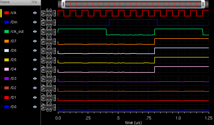
The third simulation shows the binary number 11110000 (240) being fed into the
converter. The number is then outputted on the output lines with D7 being the
most significant bit, after clk_out (clock divided by
8) goes high.
These
simulations show examples of the converter working as intended.
All of the files for the first half of this project can be found in the
following link: proj_f18_ds
This concludes the first part of the project.
2) 2nd Half
of Project Description
-The second
half of the project required the student to create a complete layout for the
8-bit serial-to-parallel converter and document the process.
-The first
initial layouts that were created were for the inverter and transmission gate
(TG).
Inverter symbol: TG symbol:
Inverter layout: Inverter extracted view: TG layout: TG extracted
view:
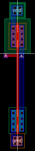
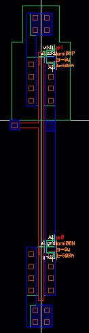
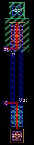
-The TG and
the inverter layouts were used to create the layout of the edge triggered D
flip-flop.
Edge triggered D flip-flop (DFF) symbol:
Edge triggered D flip-flop (DFF)
layout:
Edge triggered D flip-flop (DFF)
extracted view:
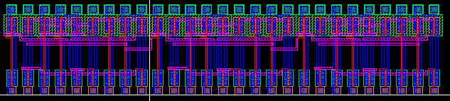
- The next step
was to create the 8-bit shift register and 8-bit hold register using the layout
of the DFF. These registers are used in the final layout of the converter.
Shift register layout:

Shift register extracted view:

Hold register layout:

Hold register extracted view:

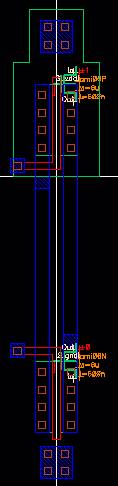
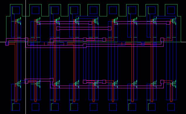
- One of the
last pieces the student designed before assembling the complete converter
layout is the layout of the clock divider.
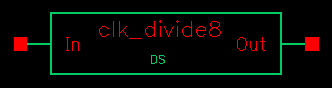
Clock divider symbol:
Clock divider layout:
Clock divider extracted view:
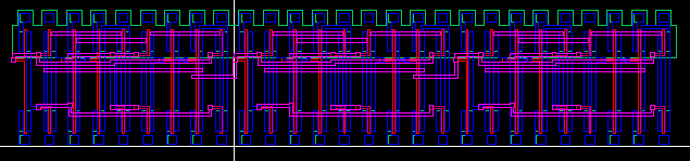
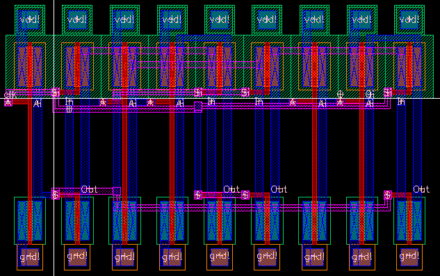
- The last procedure
the student went through was combining the previous layouts and wiring them
together to finalize the complete layout of the 8-bit serial-to-parallel
converter.
Converter symbol:
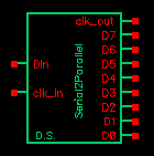
8-bit serial-to-parallel converter
layout:
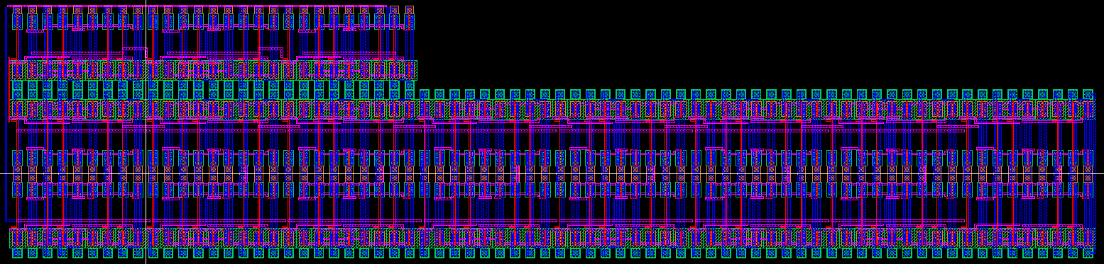
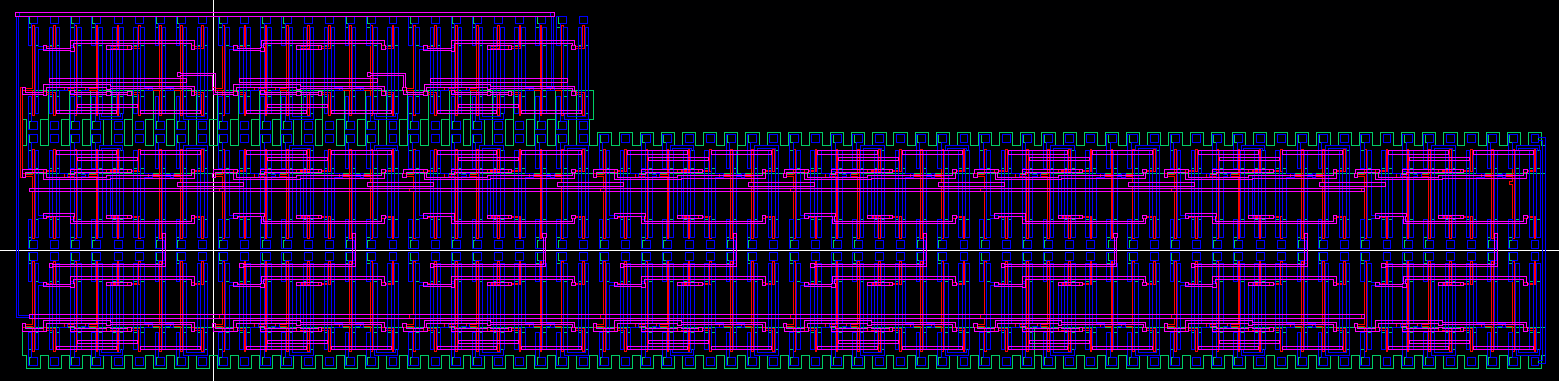
8-bit serial-to-parallel converter
extracted view:
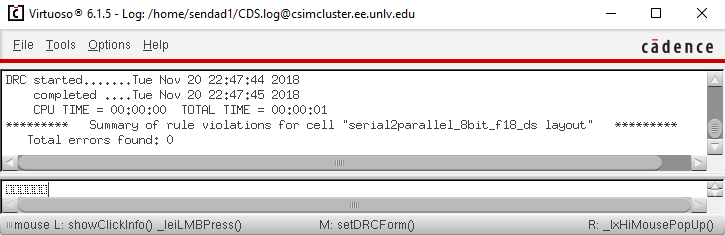
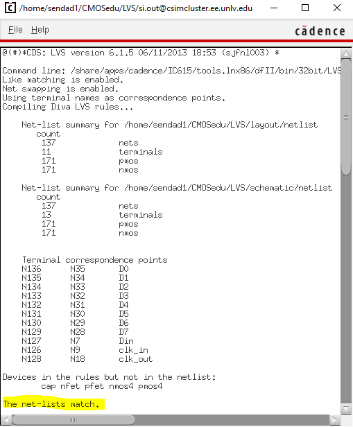
- Throughout
the process of creating all of the pieces for the converter, the student was
doing various design rule checks (DRCs) and layout versus schematic (LVS)
checks in order to ensure correct and accurate layouts. Only the very last DRC
and LVS check of the finalized converter layout will be included because those
alone prove that everything else also passed the DRC and LVS checks.
8-bit serial-to-parallel converter DRC
results:
8-bit serial-to-parallel converter
LVS results:
All of the
files for the entire project can be found in the following link: proj_f18_ds
This concludes the first part of the project.
Additional Links
→ Return to listing of
lab reports
→ Daniel’s CMOS
homepage
→
Dr. Baker’s CMOS homepage