 Lab 5 – EE 421L
Authored by: Daniel Senda
Email: sendad1@unlv.nevada.edu
Fall 2018
Due: 10-10-2018
1) Pre-Lab Description
The first
task is to back-up all of the previous work from the previous lab.
The second task
was to go through and finish tutorial 3.
- Tutorial 3 goes over the design, layout, and simulation of a CMOS inverter.
2) Description of Lab
Procedures
This lab
had the student create schematics, layouts, and symbols for two different
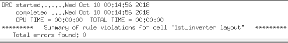
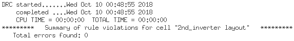
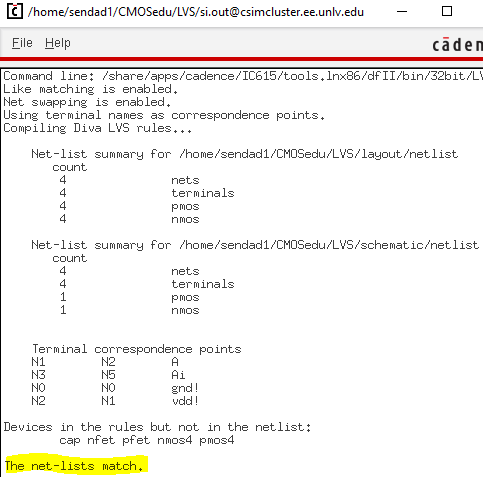
configurations of an inverter. In addition, the student had to run a DRC and a
LVS process to ensure that the layout and schematic correspond to each other
for both inverters.
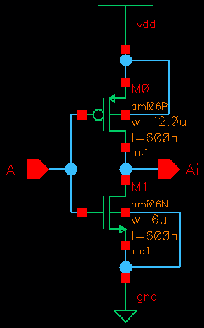
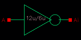
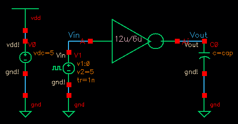
The first inverter had the following
requirements:
- PMOS Width-to-length ratio: 12µm/0.6µm
- NMOS Width-to-length ratio: 6µm/0.6µm
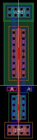
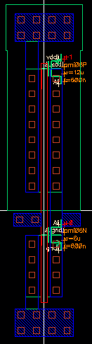
First inverter schematic Layout view Extracted
view
Layout DRC results
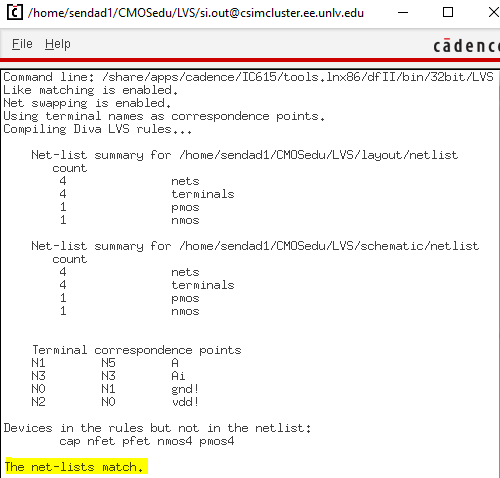
LVS results
First inverter schematic symbol
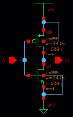
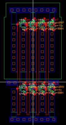
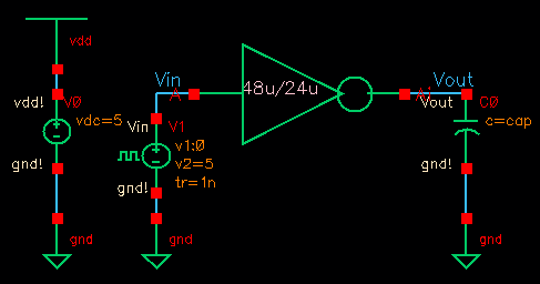
The second
inverter had the following requirements:
- PMOS
Width-to-length ratio: 48µm/0.6µm
(* 12µm/0.6µm)
- NMOS Width-to-length ratio: 24µm/0.6µm (* 6µm/0.6µm)
- Multiplier for both MOSFETS: 4 (* Since the multiplier is 4, the MOSFET widths
become ![]() )
)
Second inverter schematic
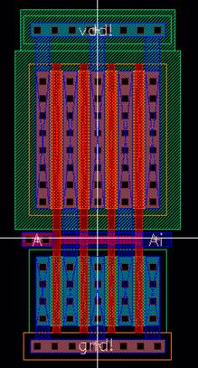
Layout view
Extracted view
DRC Results
LVS Results
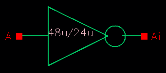
Second inverter schematic symbol
In addition to creating the inverter files shown
above, the student also had to simulate the inverters to ensure correct
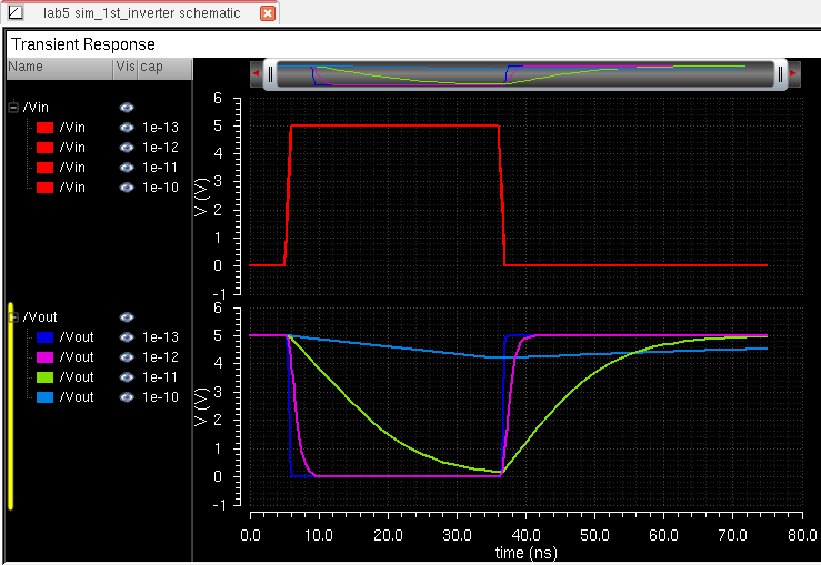
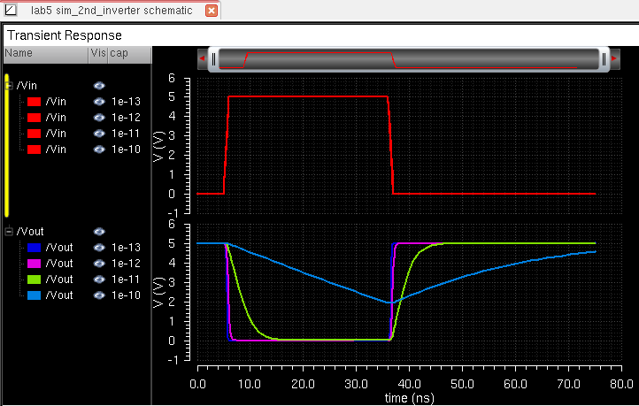
operation. Students were first required to simulate both inverters using SPICE,
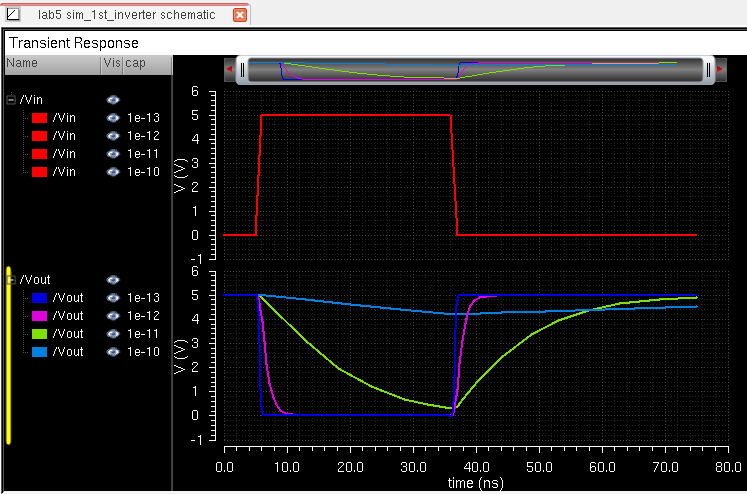
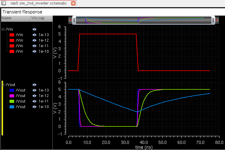
each driving a 100 fF, 1 pF, 10 pF, and 100 pF capacitive load.
Simulation set-up schematic of first inverter
SPICE simulation results of first inverter
Simulation set-up schematic of second inverter
SPICE simulation results of first inverter
Students
were lastly required to simulate both inverters using UltraSim
(A faster simulator than SPICE at the cost of accuracy), each driving a 100 fF, 1 pF, 10 pF, and 100 pF capacitive load.
UltraSim simulation results of first
inverter
UltraSim simulation results of second
inverter
This
concludes the procedure of lab 5.
The cadence
library folder for this lab put into a zip file in order for the grader to
examine the student’s work. The zip file can be downloaded from the following
link:
lab5_ds.zip
Additional Links
→ Return to listing of
lab reports
→ Daniel’s CMOS
homepage
→
Dr. Baker’s CMOS homepage