 Lab 4 – EE 421L
Authored by: Daniel Senda
Email: sendad1@unlv.nevada.edu
Fall 2018
Due: 09-26-2018
1) Pre-Lab Description
The first task is to back-up all of the previous work from the
previous lab.
The second task was to go through and finish tutorial 2.
- Tutorial 2 covers the layout and simulation of the IV curves of PMOS and NMOS
devices.
2) Description of Lab
Procedures
The first
procedures of this lab had the student generate four schematics along with
appropriate simulations.
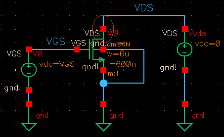
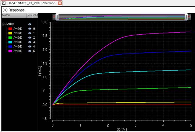
The first schematic is simulating ID vs.
VDS of an NMOS device. It has the following parameter requirements:
- VGS: Varies from (0 – 5 V)
in 1V steps.
- VDS: Varies from (0 – 5 V) in 1mV steps.
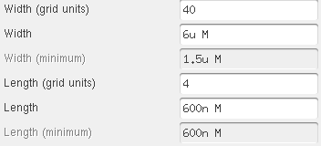
- Width-to-length ratio: 6µm/600nm.
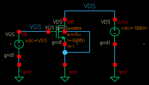
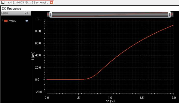
The second schematic is simulating ID vs.
VGS of an NMOS device. It has the following parameter requirements:
- VGS: Varies from (0 – 2 V)
in 1mV steps.
- VDS: 100 mV.
- Width-to-length ratio: 6µm/600nm.
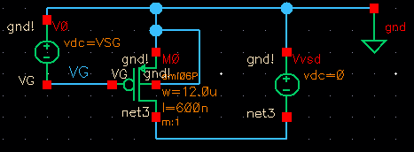
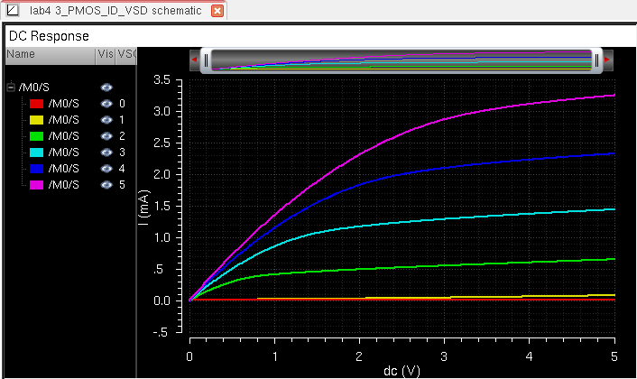
The third schematic is simulating ID vs.
VSD (note VSD not VDS) of a PMOS device. It has the following parameter
requirements:
- VSG: Varies from (0 – 5 V)
in 1V steps.
- VSD: Varies from (0 – 5 V) in 1mV steps.
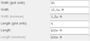
- Width-to-length ratio: 12µm/600nm.
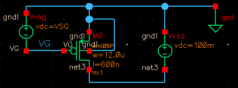
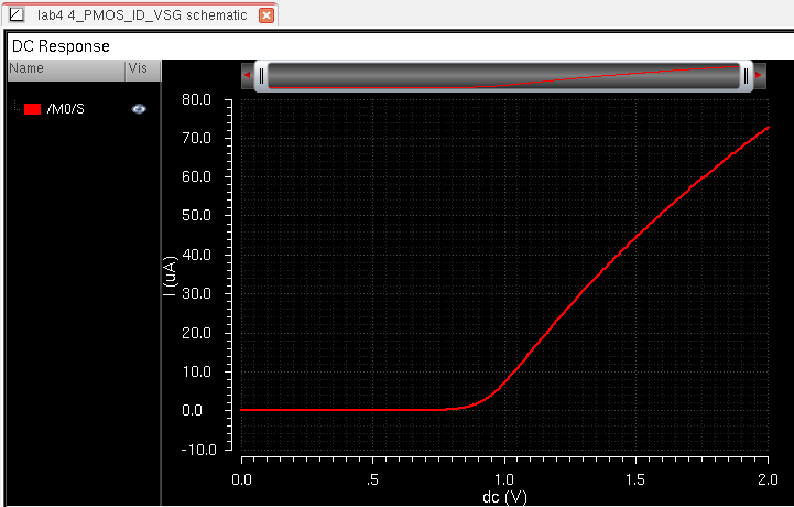
Lastly, the fourth schematic is simulating ID vs.
VSG of a PMOS device. It has the following parameter requirements:
- VSG: Varies from (0 – 2 V)
in 1mV steps.
- VSD: 100 mV.
- Width-to-length ratio: 12µm/600nm.
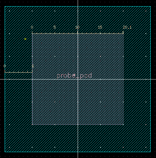
Next, the
student was required to layout 4 terminal NMOS and PMOS devices with probe pads.
The first step was to create the probe pad layout, schematic, and symbol.
The probe pad had to follow MOSIS design
rules. The following rules apply to probe pads:
- (Rule 10.2) States that the minimum probe passivation opening is 20 microns.
- (Rule 10.3) States that pad metal overlap of passivation has to be 6 microns
or greater.
- The probe pad must be created on the topmost metal
layer, which in this case is metal3.
Layout
Schematic

Schematic Symbol
 f
f
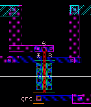
The NMOS device had the following requirements:
- Width-to-length ratio: 6µm/0.6µm.
- 4 MOSFET terminals that connect to probe pads.
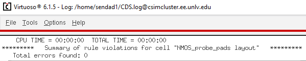
- Show successful layout DRC (Design Rule Check).
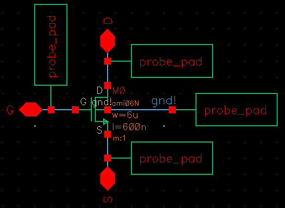
- Create corresponding schematic.
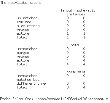
- Show successful LVS (layout versus schematic) check.
Layout
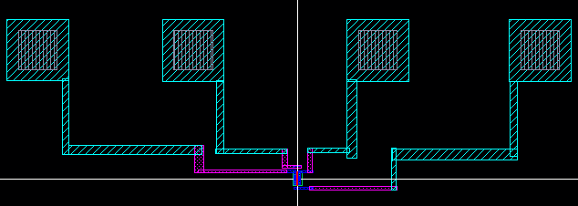
Zoomed-in layout
Successful DRC
Schematic
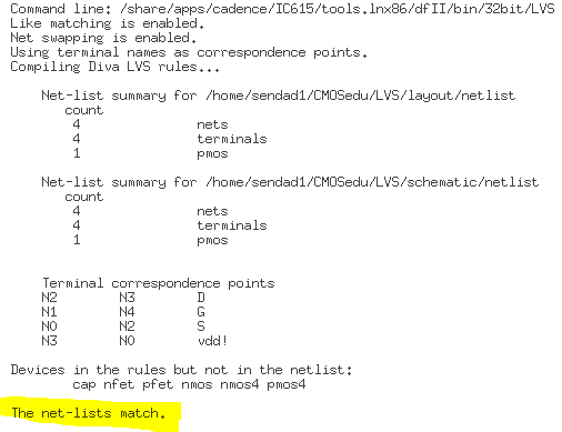
Successful LVS
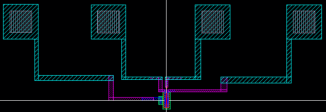
The PMOS device had the following
requirements:
- Width-to-length ratio: 12µm/0.6µm.
- 4 MOSFET terminals that connect to probe pads.
- Show successful layout DRC (Design Rule Check).
- Create corresponding schematic.
- Show successful LVS (layout versus schematic) check.
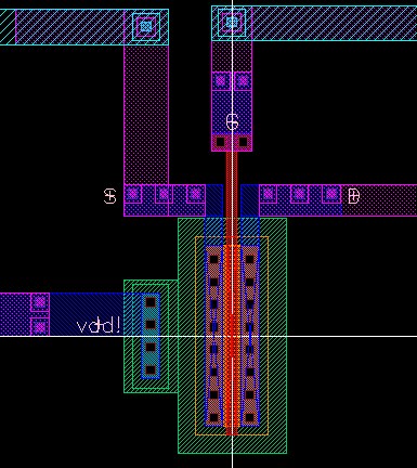
Layout
Zoomed-In Layout
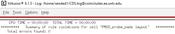
Successful DRC
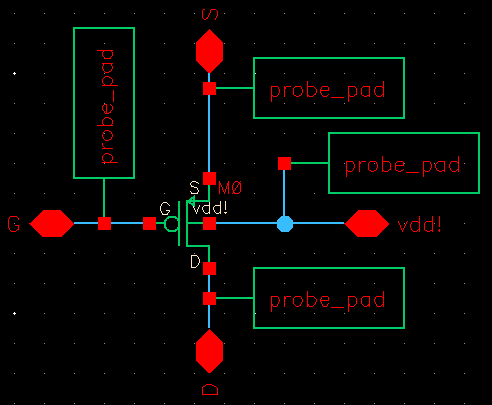
Schematic
Successful LVS
This
concludes the lab 4.
Additional Links
→ Return to listing of
lab reports
→ Daniel’s CMOS
homepage
→
Dr. Baker’s CMOS homepage