 Lab 3 – EE 421L
Authored by: Daniel Senda
Email: sendad1@unlv.nevada.edu
Fall 2018
Due: 09-19-2018
2) Pre-Lab Description
The first
task is to back-up all of the previous work from the lab.
The second
task was to finish tutorial 1.
The remaining part of tutorial 1 dealt with creating the layout of a resistor
and going through the proper procedures up to running the LVS (layout versus
schematic) check to assure that the schematic matched up with the layout.
3) Description of Lab
Procedures
The lab
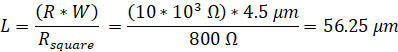
instructs students to create a 10k resistor using the n-well. In addition, it
has to be created referencing process information from MOSIS. MOSIS is an
integrated circuit fabrication service that uses the C5 process, so the
resistor was created using the C5 process parameters and guidelines. The sheet
resistance of the n-well is roughly 800 ohms. The minimum width of the n-well
is 3.6 microns (micro meters). The following formula will be used to select
appropriate width and length values.
R = 10 kΩ. Rsquare = 800 Ω.
Let W = 3.6 microns. Will solve for the value of L.
The resistor was laid out using the above parameters. Once extracted, the
resistor value was off by a few ohms. The length was adjusted manually to get a
more precise value. The length that gave the most precise value was L = 54.96 µm. Down below is a snip of the full resistor in the layout
editor window.
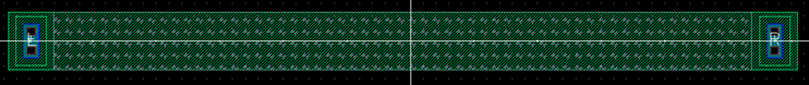
Zoomed-in layout
view:
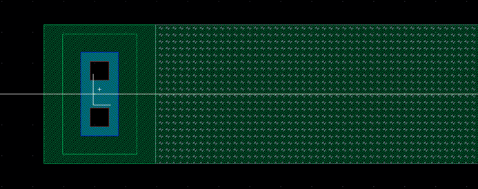
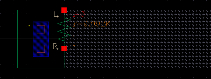
The resistor
went through the DRC (design rule check) and resulted in zero errors. It was
then extracted successfully. Zoomed-in extracted view:
Next, the
students had to create a layout for the DAC from lab 2 using this 10k resistor.
The lab instructions required all of the resistors to be precisely stacked on
top of each other with enough space between them to prevent DRC errors. The
following picture shows the full DAC layout.
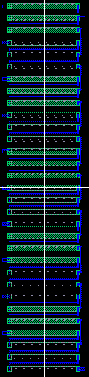
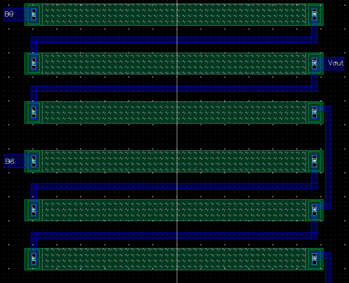
This is a
zoomed-in image of the completed DAC layout including the specified 10k
resistor, appropriate metal1 routings, and pins.
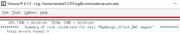
After it was
completed, the layout went through the DRC and resulted in 0 errors.
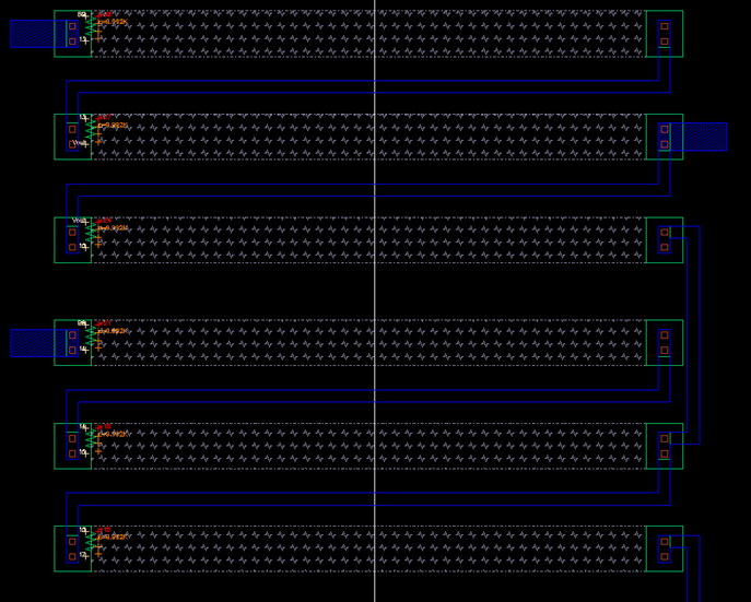
The DAC
layout was then extracted.
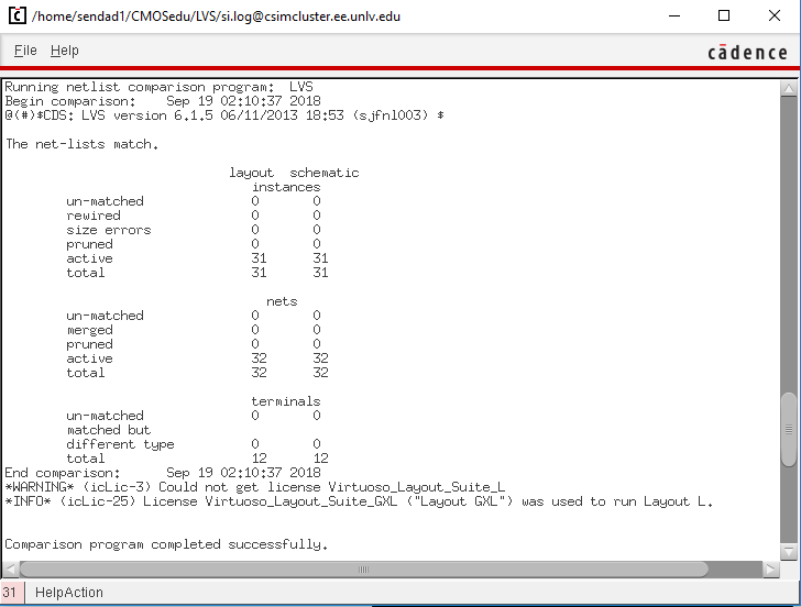
Lastly, the
DAC design went through the LVS check. The netlists matched as can be seen on
the results log.
The cadence
library folder for this lab was made into a zip file in order for the grader to
examine the student’s work. The zip file can be downloaded from the following
link:
Lab3.zip
Additional Links
→ Return to listing of
lab reports
→ Daniel’s CMOS
homepage
→
Dr. Baker’s CMOS homepage