 Lab 2 – EE 421L
Authored by: Daniel Senda
Email: sendad1@unlv.nevada.edu
Fall 2018
Due: 09-12-2018
1) Pre-Lab Description
The prelab
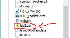
consisted of several tasks. The first thing that needed to be done was to
download the lab2.zip file from the CMOSedu webpage.
The file was then uploaded to the student’s CMOSedu
directory as seen below. Afterwards, the file was unzipped in order to access
the contents inside the folder.
 →
→ 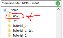
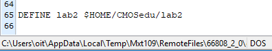
The lab2
folder is a library that has to be defined in the cds.lib text file in order
for cadence to be able to open it.
Cadence was started and the ideal 10-bit ADC and DAC schematic was opened
from the lab2 library.
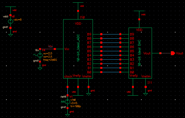
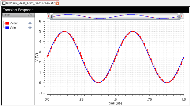
The
simulation of the schematic was ran using the saved state which resulted in the
following waveform.
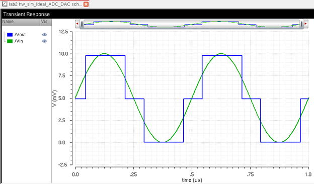
The
schematic was modified in order to get a different waveform from the
simulation. The magnitude of Vin was changed from 2.5
V to 5mV. The VREF voltage stayed the same, thus the 1 LSB value
also stayed the same. 1 LSB is the least significant bit, which is the smallest
possible change in the analog output voltage.
![]()
In other words, the value of one step is 4.88 mV. Thus, one step is sufficient
to go from 5mV to 10mV as can be seen below.
2) Description of Lab
Procedures
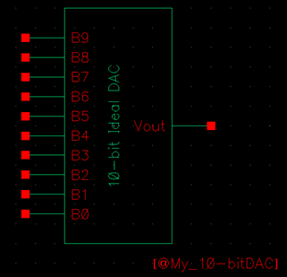
The following pictures show the schematic diagram and symbol of the
created 10-bit DAC.
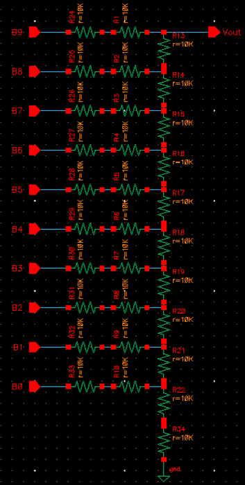
In order to
determine the output resistance, some calculations need to be made. The first
step is to connect all the B inputs to ground in the schematic above. Then, by
using the resistors in parallel formula, you simplify down the resistors until
you reach the total output resistance.
![]()
After simplifying it down ten times, the output resistance ends up being Routput = 10kΩ.
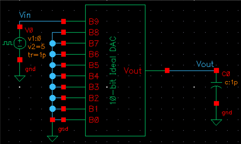
Driving a
load using the DAC is the next procedure. The tasks requires the student to
find the delay when driving a 10pF capacitive load. The following image shows
the schematic.
![]()
![]()
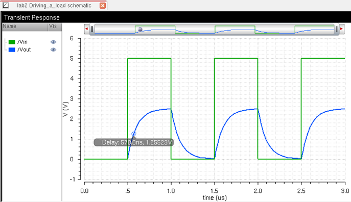
The following is the load simulation showing the DAC delay.
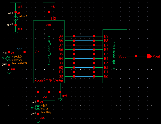
Next step in the procedure is to replace the ideal DAC with the one made
by the student.
Additional Links
→ Return to listing of
lab reports
→ Daniel’s CMOS
homepage
→
Dr. Baker’s CMOS homepage