Lab 4 - EE 421L
Authored
by Marco Muniz,
Email: munizm1@unlv.nevada.edu
09/24/2018
Pre-Lab
The prelab consisted of:
- Learning how to create a NMOS Schematic and Layout.
- Learning how to create a PMOS schematic and Layout.
- Learning to simulate the above Schematics to show IV Curves for both NMOS and PMOS.
- Showing our back up files
The pictures below will illustrate the finished schematics and layout for the above circuits.Lab
description.
Back-up File
________________________________________________________________________________________________________
Lab
The Main Lab will be seperated into three different parts.
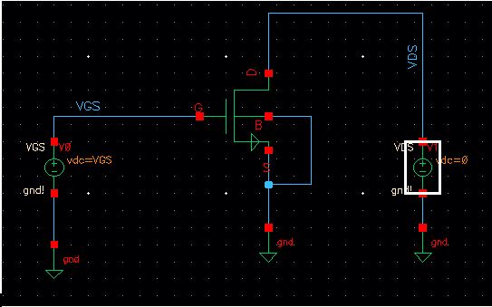
Part 1: NMOS
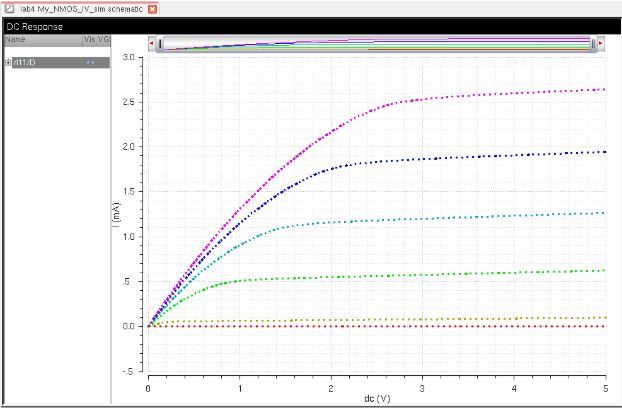
- A schematic for simulating ID
v. VDS of an NMOS device for VGS varying from 0 to 5 V in 1 V steps
while VDS varies from 0 to 5 V in 1mV steps. Use a 6u/600n width-to-length ratio.
- A
schematic for simulating ID v. VGS of an NMOS device for VDS = 100 mV
where VGS varies from 0 to 2 V in 1 mV steps. Again use a 6u/600n
width-to-length ratio.
Part 2: PMOS
- A
schematic for simulating ID v. VSD (note VSD not VDS) of a PMOS device
for VSG (not VGS) varying from 0 to 5 V in 1 V steps while VSD varies from 0 to 5 V in 1 mV steps. Use a 12u/600n width-to-length ratio.
- A
schematic for simulating ID v. VSG of a PMOS device for VSD = 100 mV
where VSG varies from 0 to 2 V in 1 mV steps. Again, use a 12u/600n width-to-length ratio.
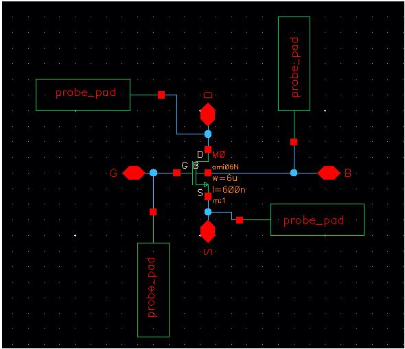
Part 3: Layouts
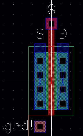
- Lay out a 6u/0.6u NMOS device and connect all 4 MOSFET terminals to probe pads.
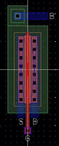
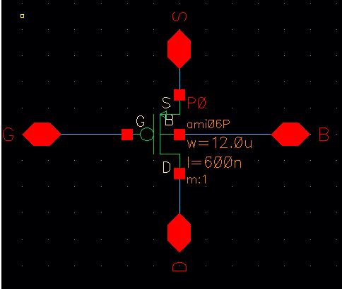
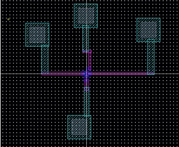
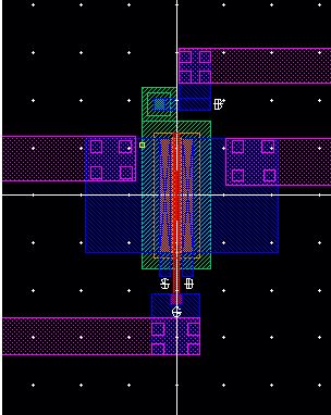
- Lay out a 12u/0.6u PMOS device and connect all 4 MOSFET terminals to probe pads.
Part 1
NMOS
Schematic for created NMOS
ID
v. VDS of an NMOS device for VGS varying from 0 to 5 V in 1 V steps
while VDS varies from 0 to 5 V in 1mV steps. Use a 6u/600n width-to-length ratio
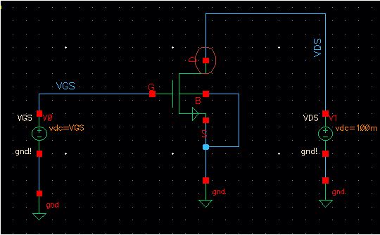
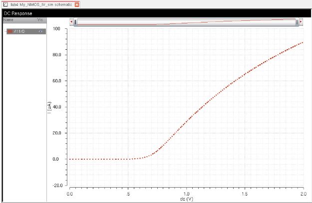
ID v. VGS of an NMOS device for VDS = 100 mV
where VGS varies from 0 to 2 V in 1 mV steps. Again use a 6u/600n
width-to-length ratio
Part 2
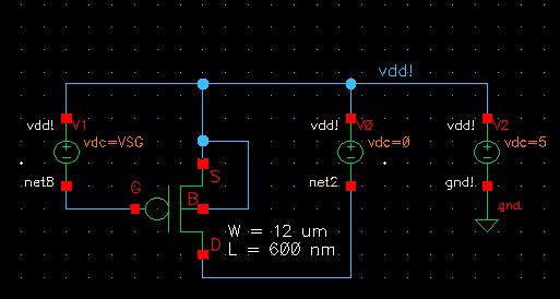
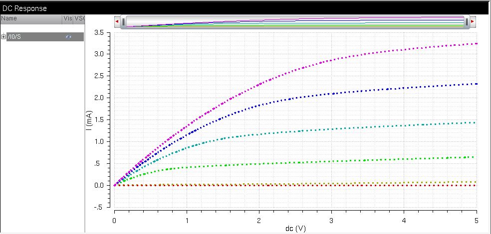
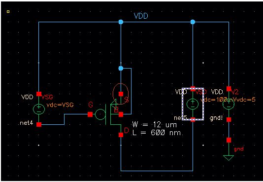
PMOS
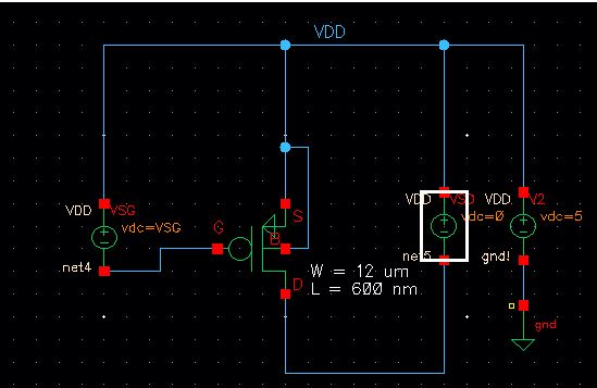
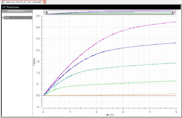
Schematic created for PMOS
ID v. VSD (note VSD not VDS) of a PMOS device
for VSG (not VGS) varying from 0 to 5 V in 1 V steps while VSD varies from 0 to 5 V in 1 mV steps. Use a 12u/600n width-to-length ratio
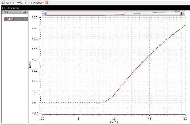
ID v. VSG of a PMOS device for VSD = 100 mV
where VSG varies from 0 to 2 V in 1 mV steps. Again, use a 12u/600n width-to-length ratio
Part 3
Lay out a 6u/0.6u NMOS device and connect all 4 MOSFET terminals to probe pads
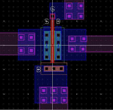
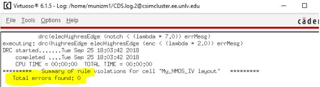
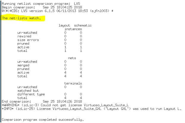
DRC and LVS verification for finished NMOS Layout below
Lay out a 12u/0.6u PMOS device and connect all 4 MOSFET terminals to probe pads
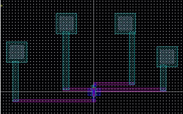
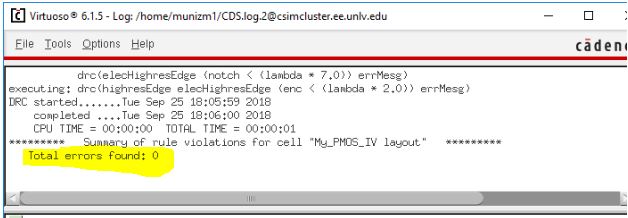
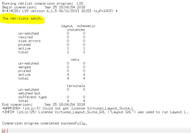
DRC and LVS verification for finished PMOS Layout below
Lab4.zip
Return to My Lab's
Return to Student Directory
Return to CMOS Home