Lab 07 - EE 421L
----------------------------------------------------------------------------------------------------
Prelab:
The labs are backed up through a saved directory in my computer as well as into my google drive account (Up-to-Date from end of previous lab).
The prelab also demonstrates Tutorial 5 on the CMOSedu website. The image size can be increased by clicking on the images for more detail.
Tutorial 5 was read previously to provide insight for the design process for connecting a wire bus to an inverter..
The following lab will use similar techniques to recreate the logic gates for 8-bit devices.
----------------------------------------------------------------------------------------------------
Lab:
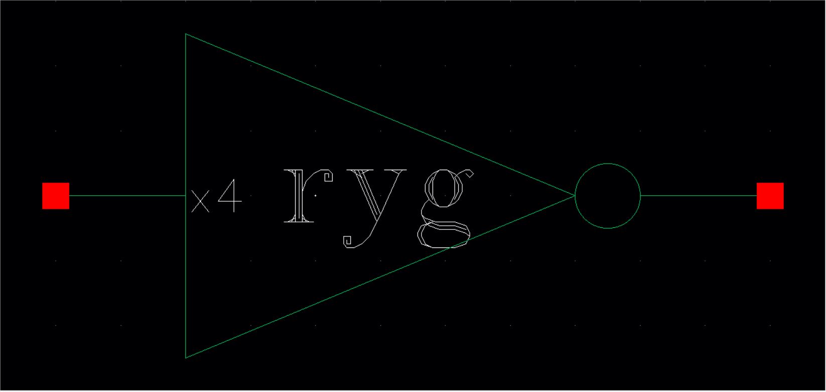
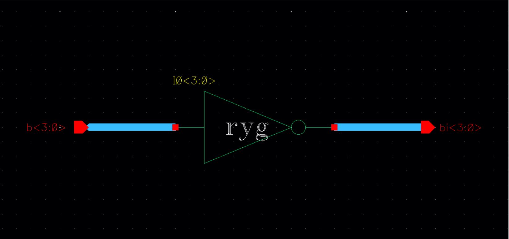
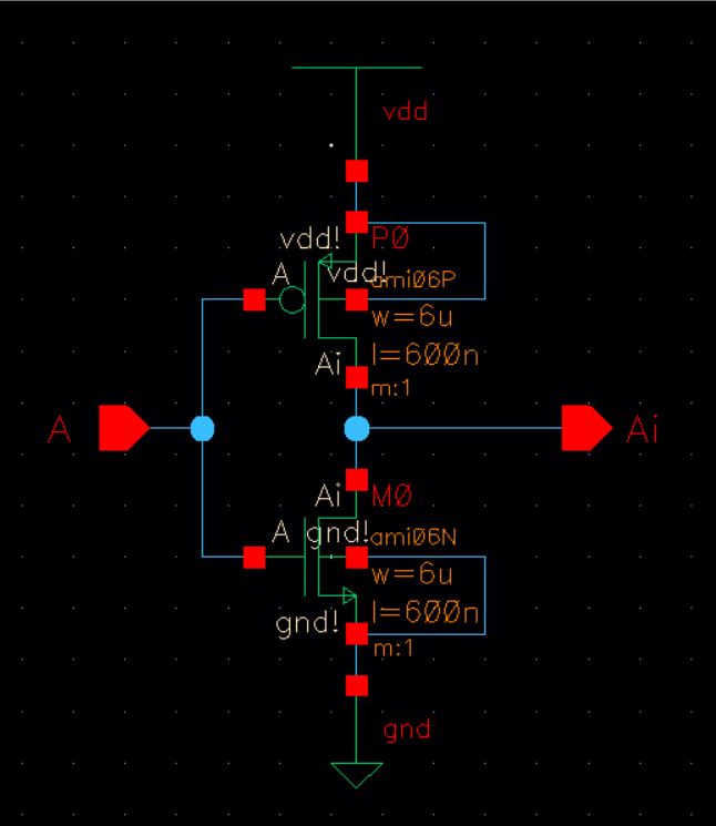
Step 1: Make an equivalent, more concise, schematic by instantiating an inverter and naming the inverter using an arrayed name (I0<3:0> see image below).
Connect a wide-wire (bus) as seen below and connect it to input and output pins. Create a symbol for the schematic.
| 4-bit Inverter Symbol | Consise 4-bit Inverter Schematic | CMOS Inverter |
| | |
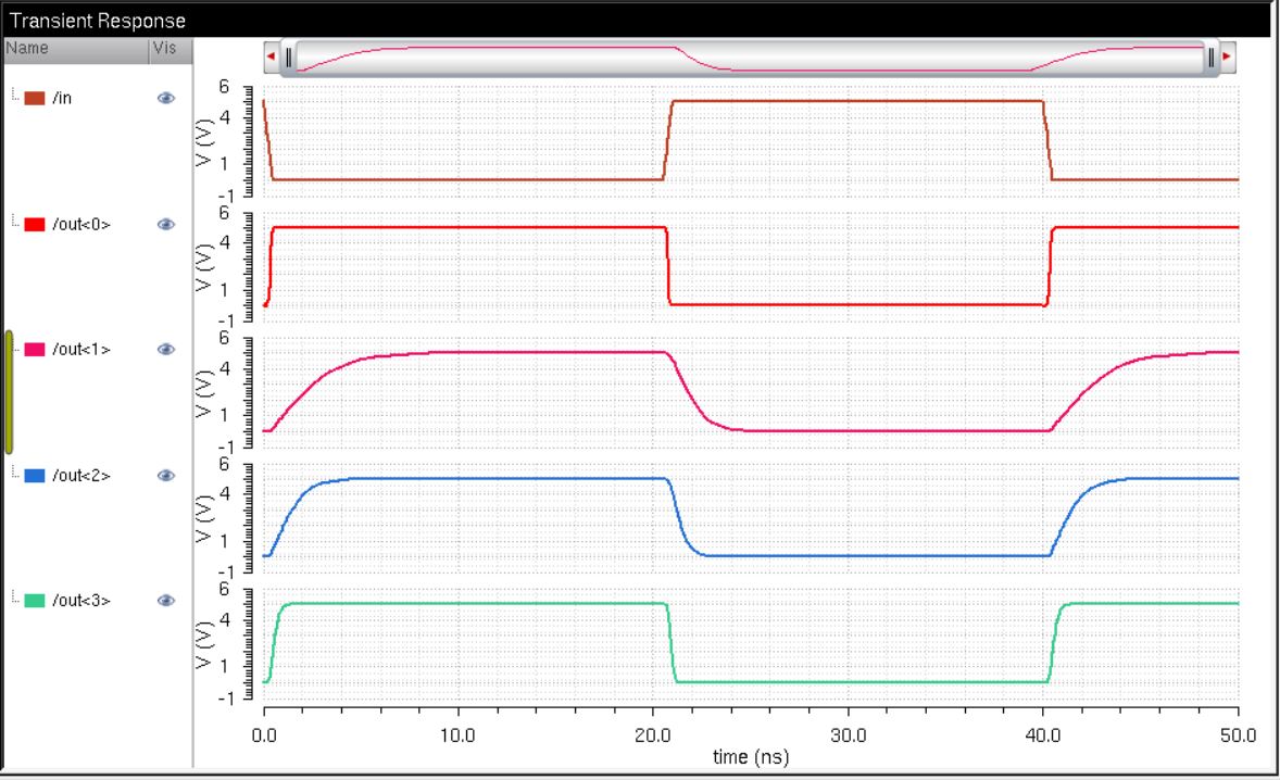
Step 2: Using this symbol create a simulation schematic. All four inverters' inputs are tied together to an input pulse source.
-> The out<0> is not connected to a load while out<3> is connected to a 100fF load.
-> The out<1> is connected to a 1 pF load while out<2> is connected to a 500 fF load.
Show, in your lab report, how a capacitive load influences the delay and rise/fall times.
| 4-bit Inverter Simulation Schematic | 4-bit Inverter Simulation Output |
 |  |
| 8-bit Symbol | Concise 8-bit Schematic | CMOS | |
| NAND | 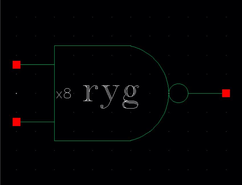 |  |  |
| AND | 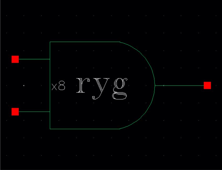 |  | 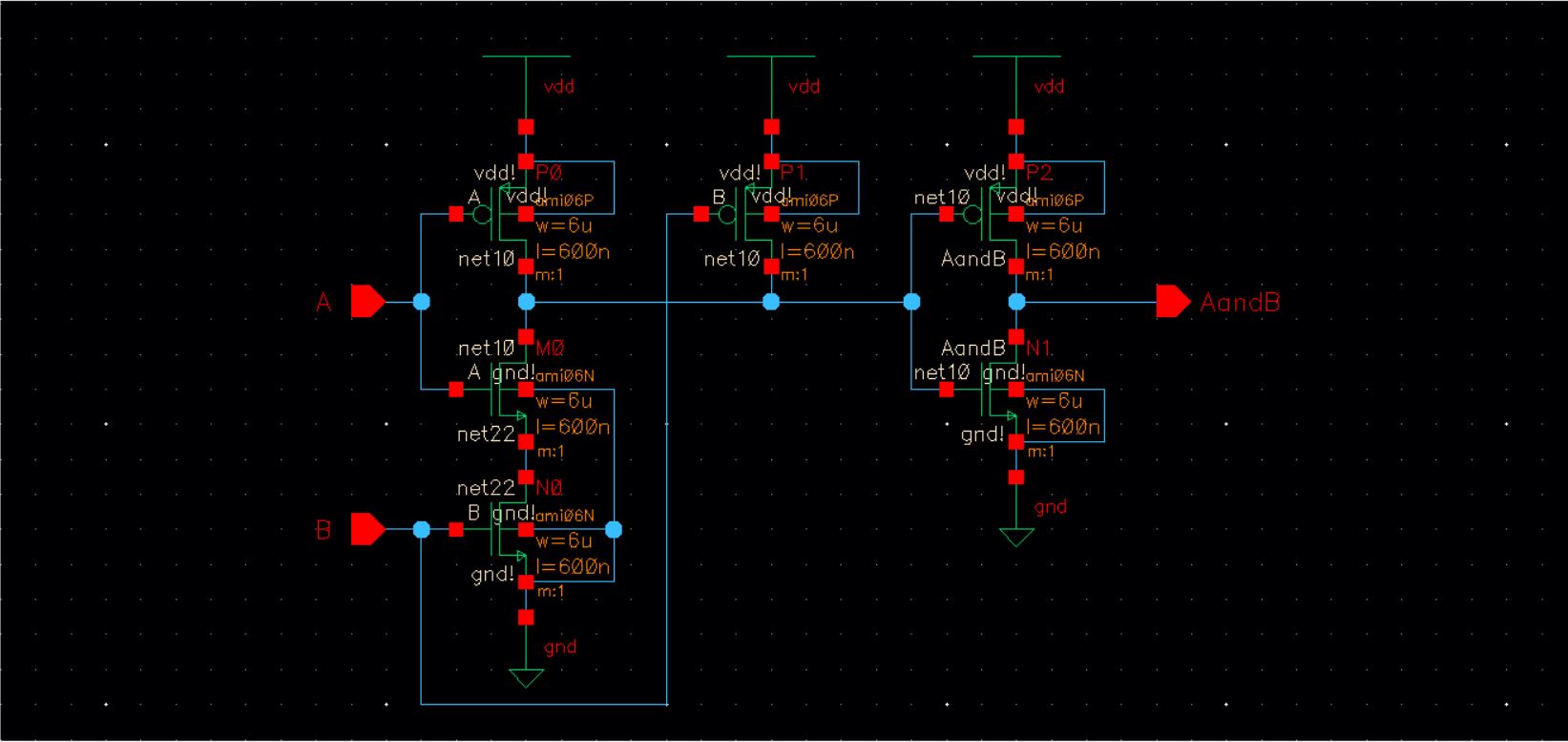 |
| NOR | 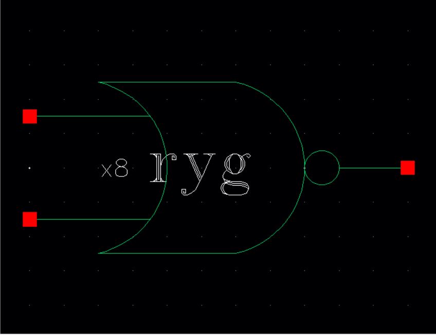 | 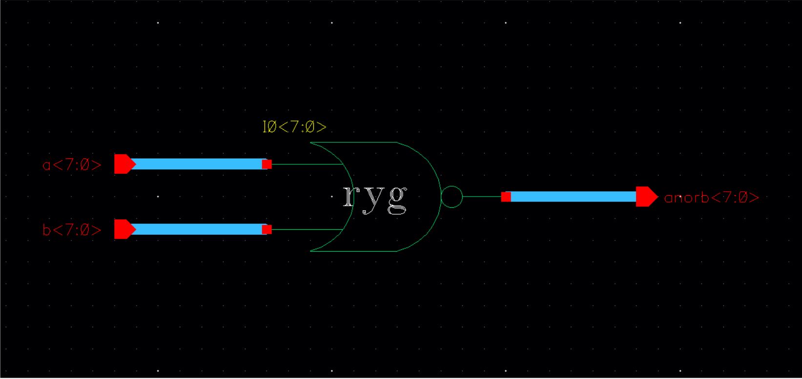 | 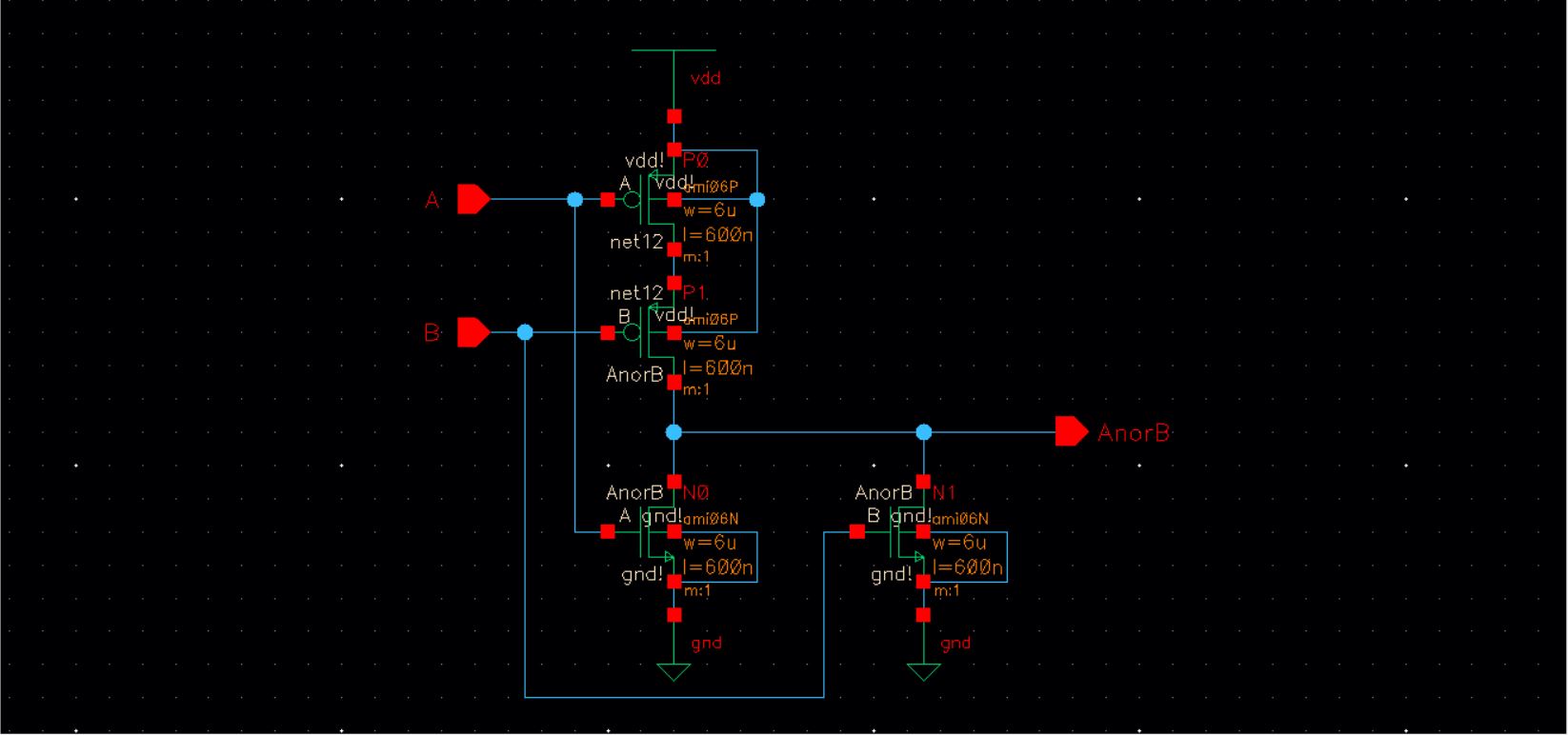 |
| OR | 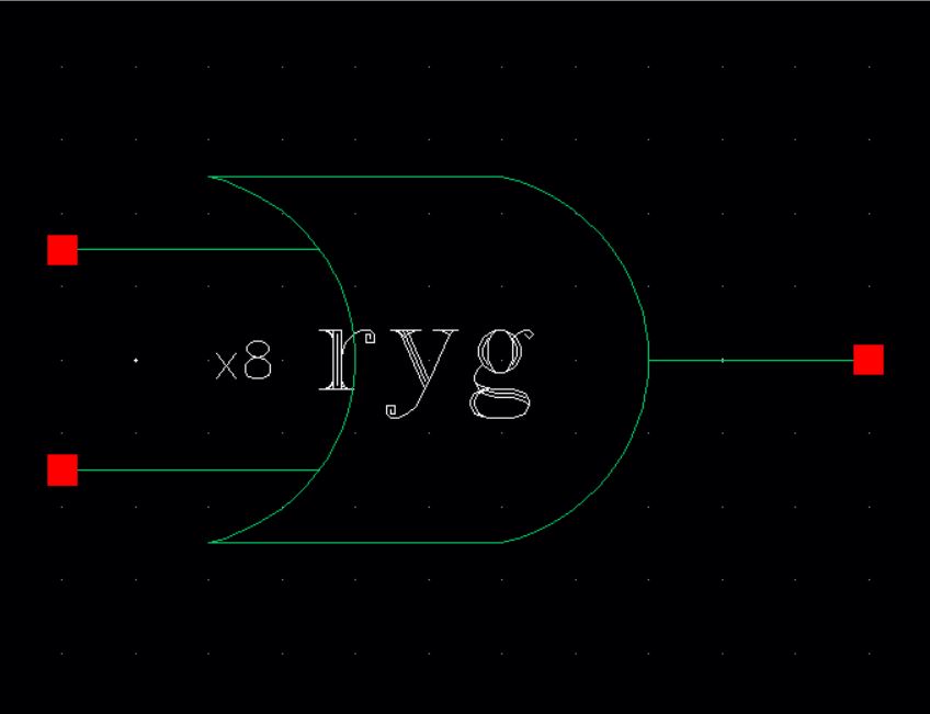 | 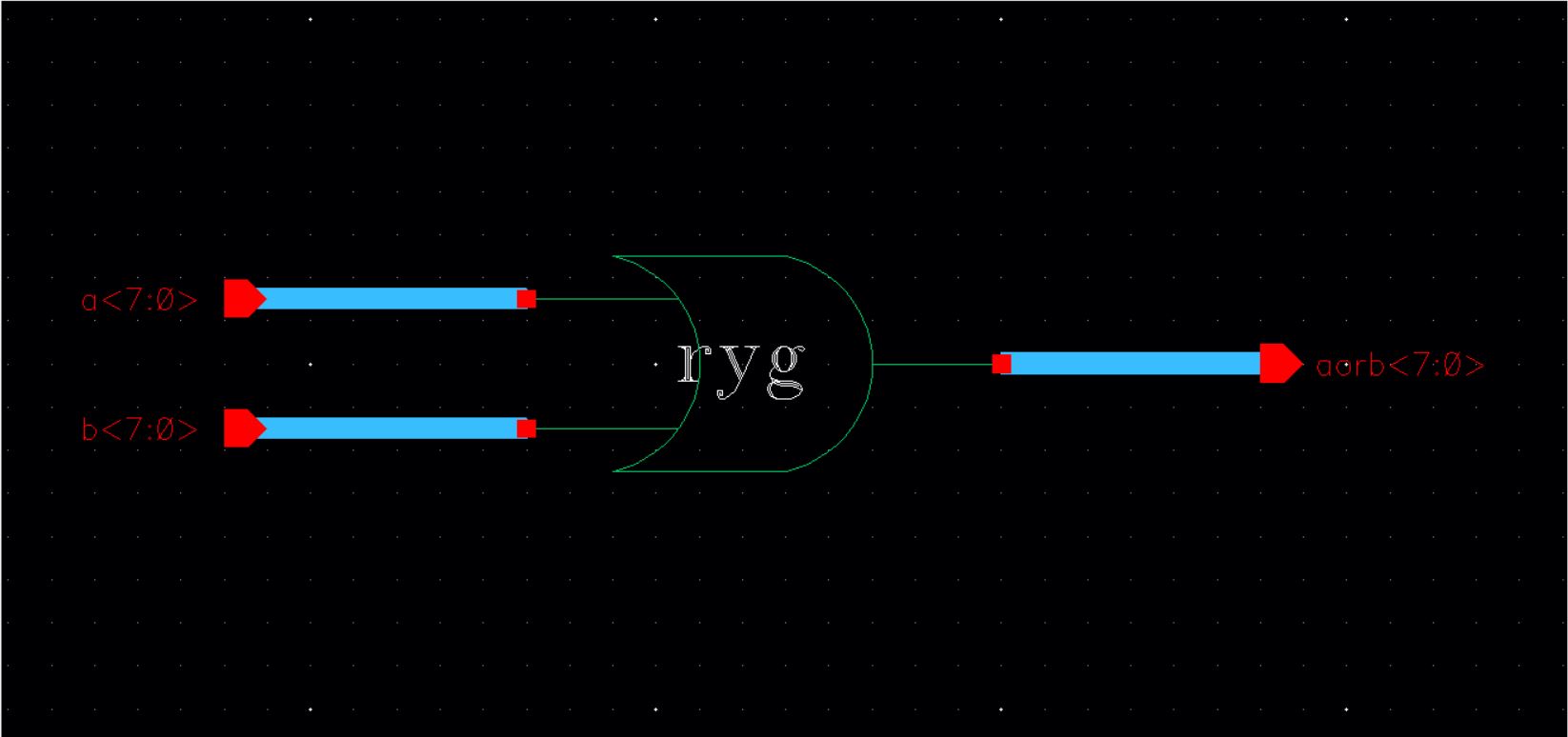 | 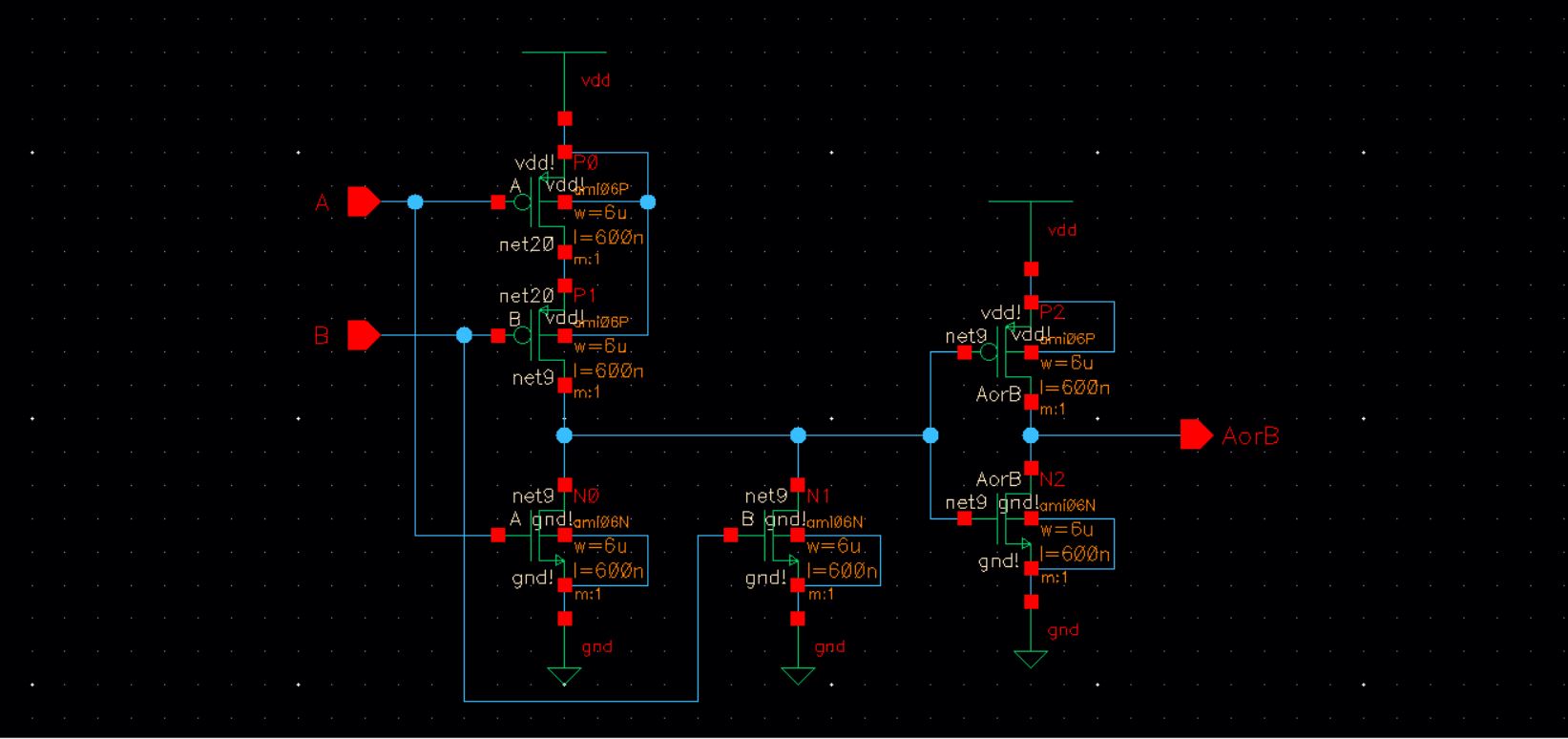 |
| Inverter |  | 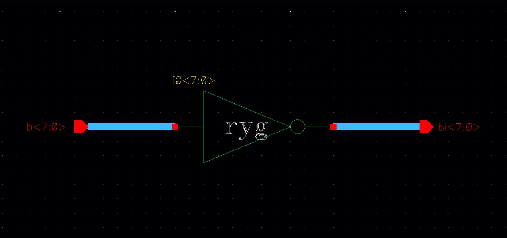 | 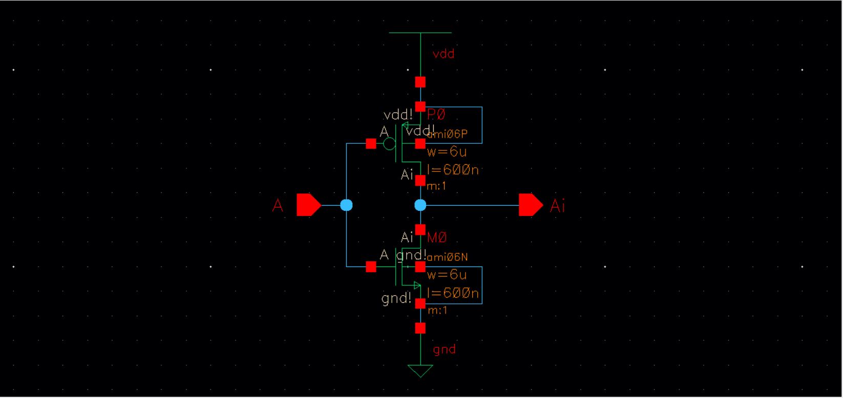 |
| 8-bit Simulation Schematic | 8-bit Simulation Output | |
| NAND |  |  |
| AND |  | 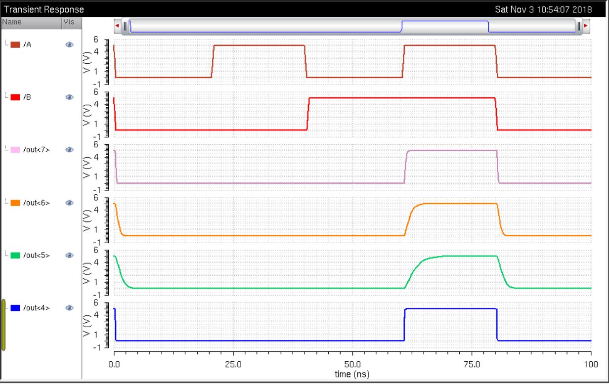 |
| NOR |  | 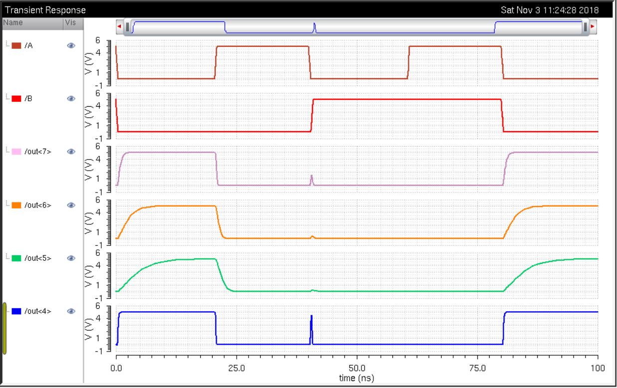 |
| OR | 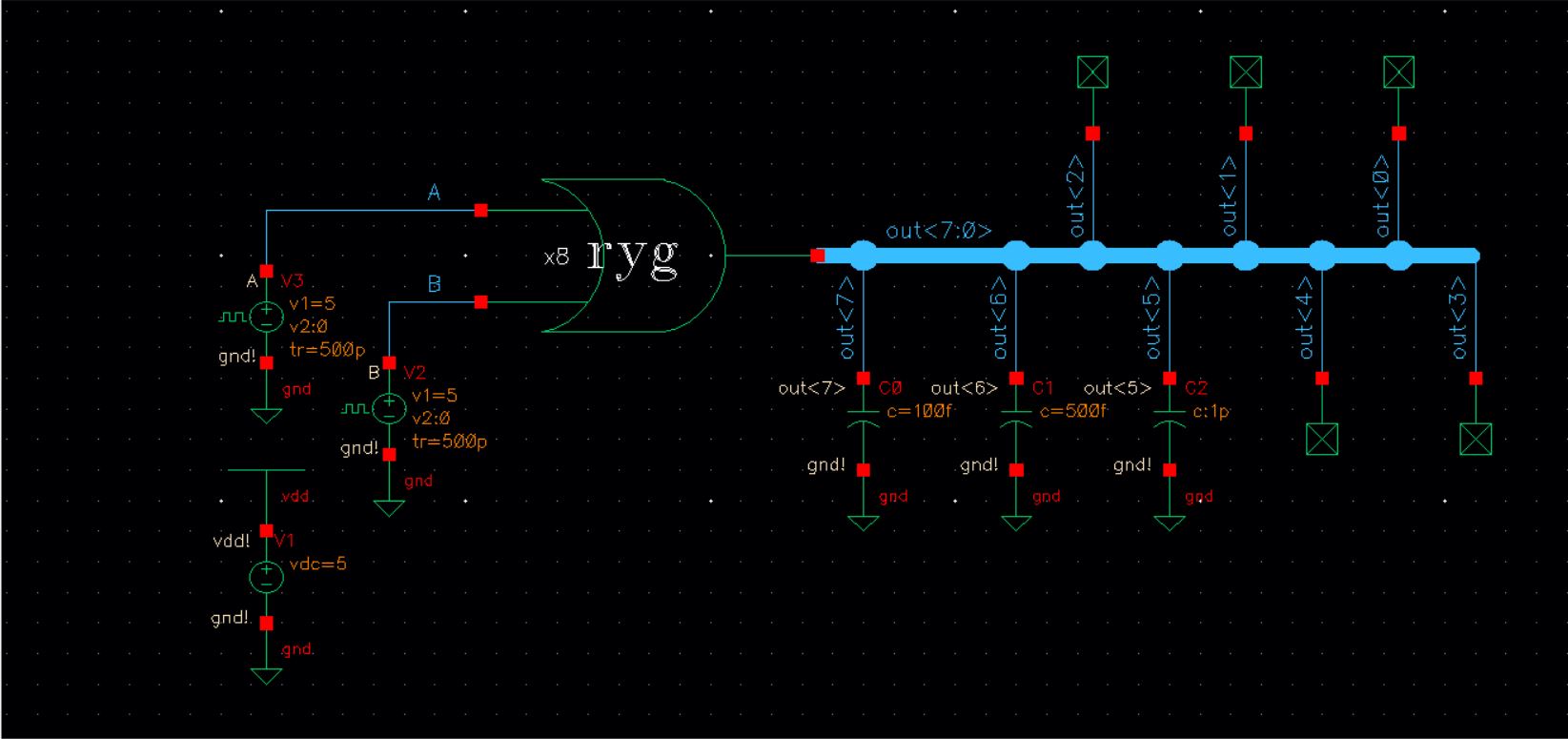 | 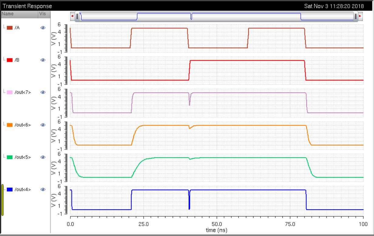 |
| Inverter |  | 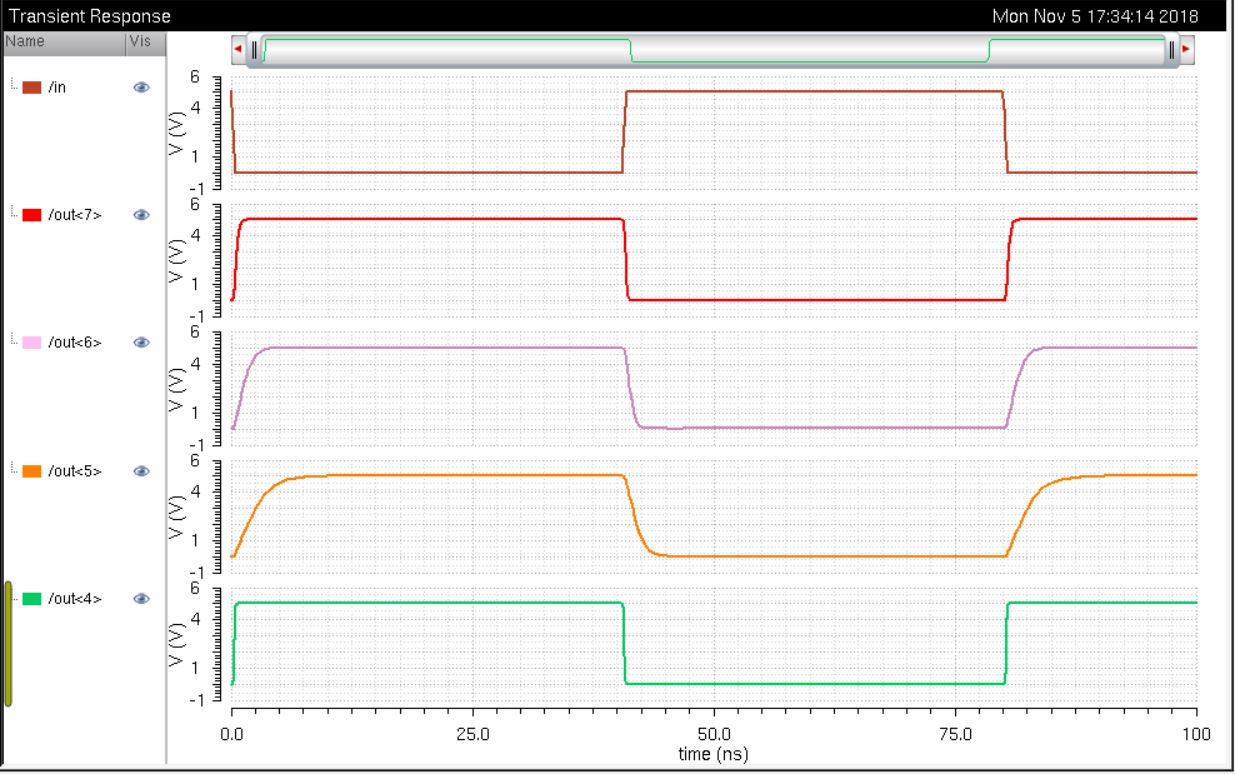 |
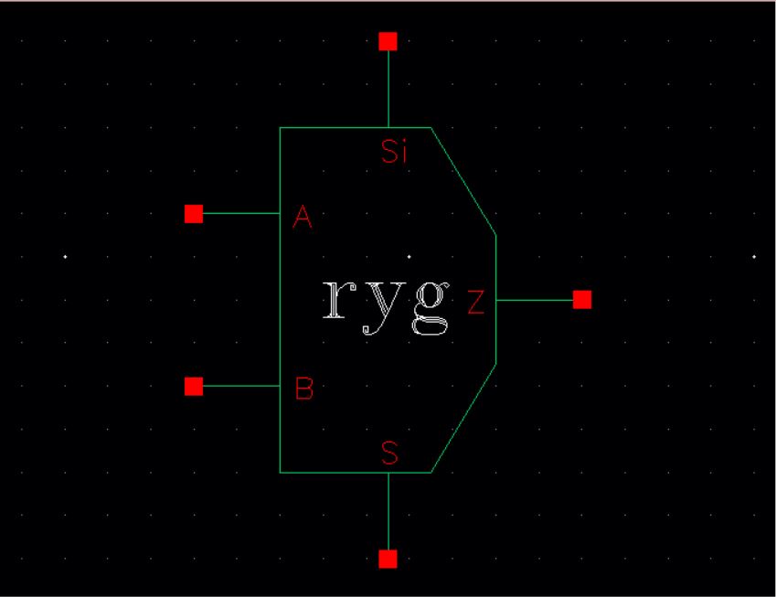
Step 3: Next examine the schematic of a 2-to-1 DEMUX/MUX (and create the symbol).
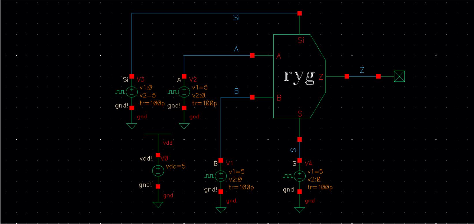
Simulate the operation of this circuit using Spectre and explain how it works.
Make sure to show, using simulations, how the circuit can be used for both multiplexing and de-multiplexing.
| MUX/DEMUX Symbol | MUX/DEMUX Schematic |
 |  |
| MUX/DEMUX SImulation Schematic | MUX/DEMUX Simulation Output |
 |  |
| 8-bit MUX/DEMUX Symbol | 8-bit MUX/DEMUX Concise Schematic |
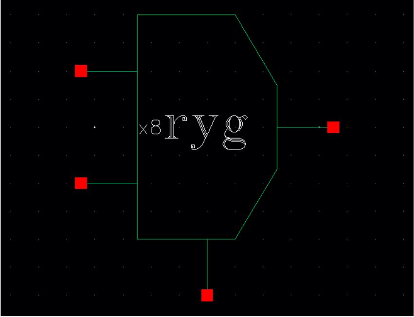 | 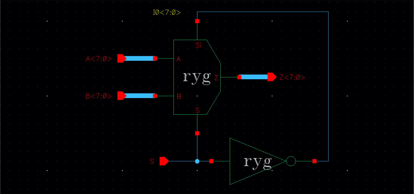 |
| 8-bit MUX Operation Simulation Schematic | 8-bit MUX Operation Simulation Output |
 |  |
| 8-bit DEMUX Operation Simulation Schematic | 8-bit DEMUX Operation Simulation Output |
|  |
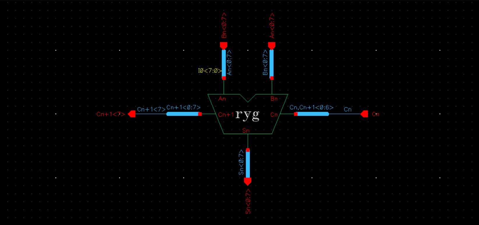
| Full Adder Symbol | Full Adder (Alternative) Schematic |
 | 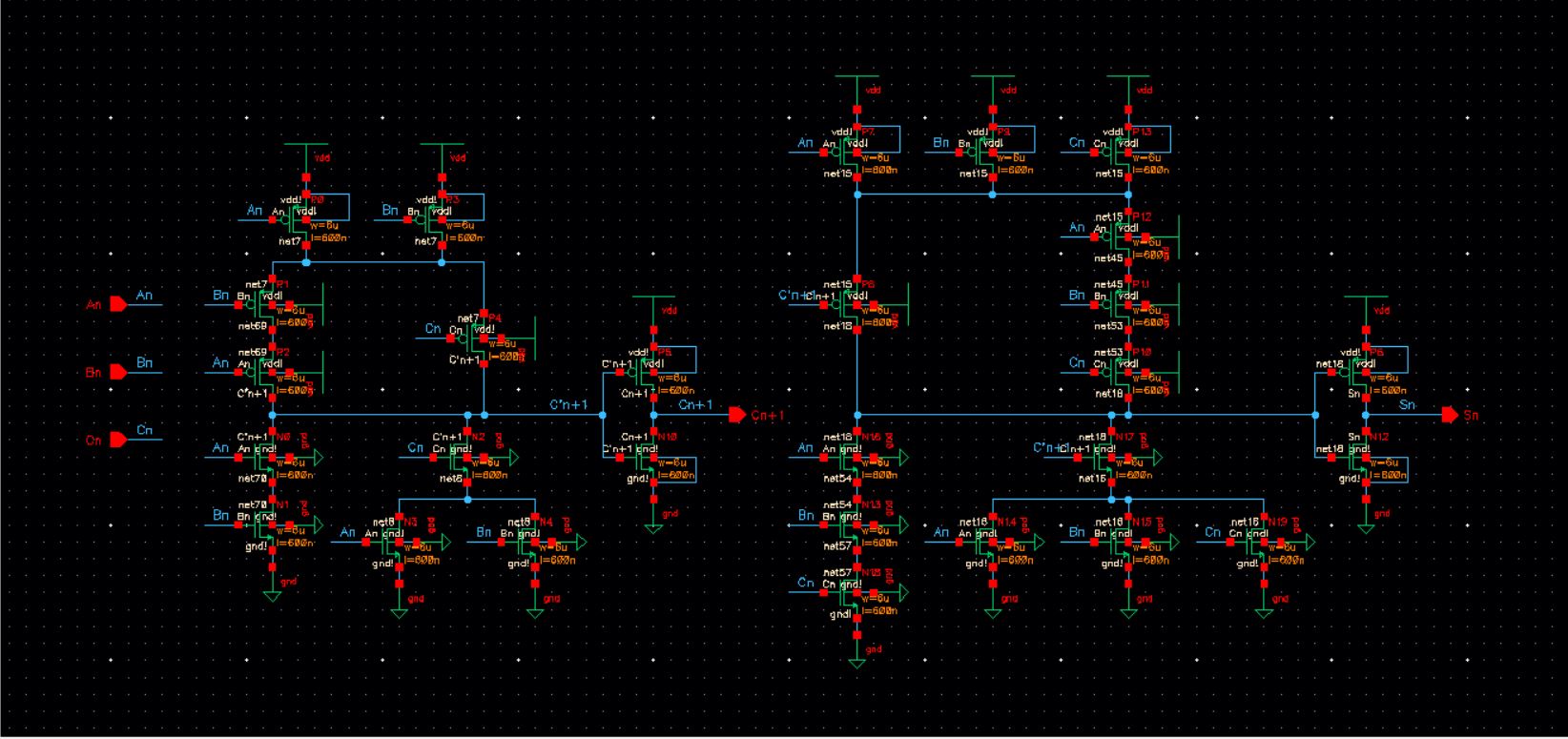 |
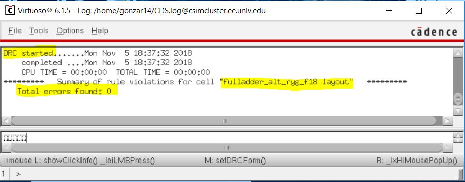
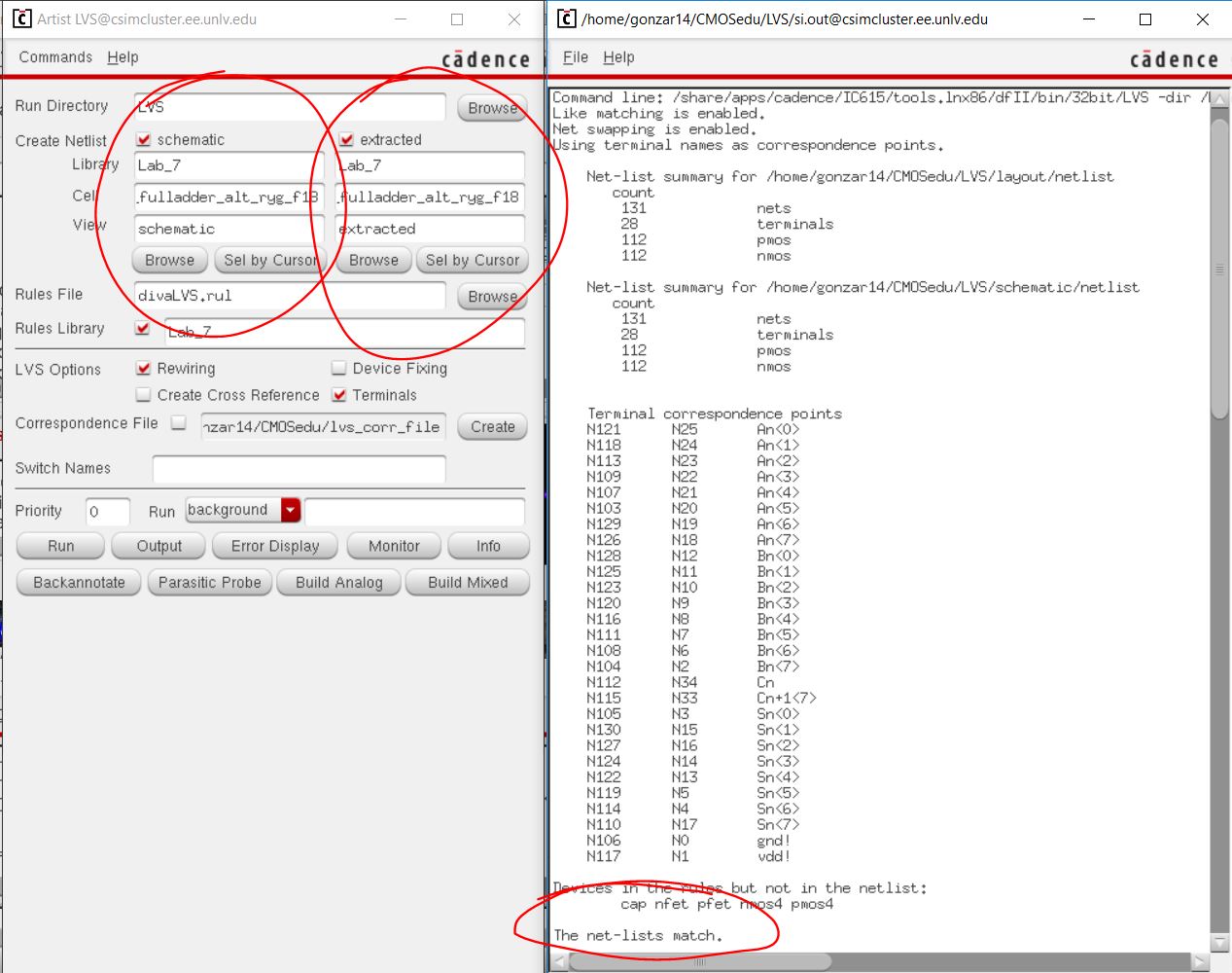
| Full Adder (Alternative) Layout | Full Adder (Alternative) Extraction |
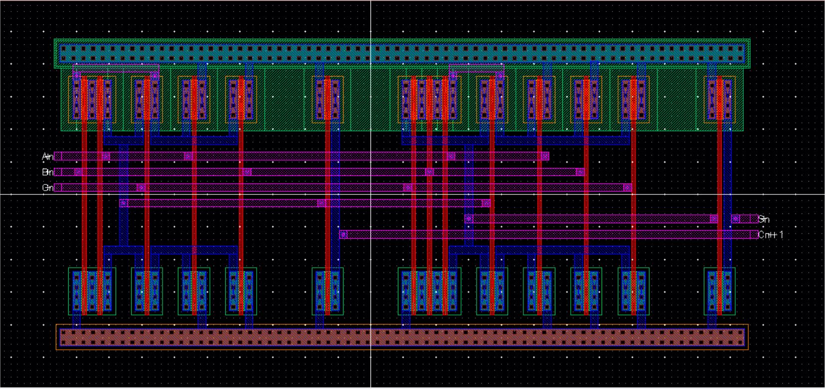 |  |
 '
'
| 8-bit Full Adder Symbol | 8-bit Full Adder Concise Schematic |
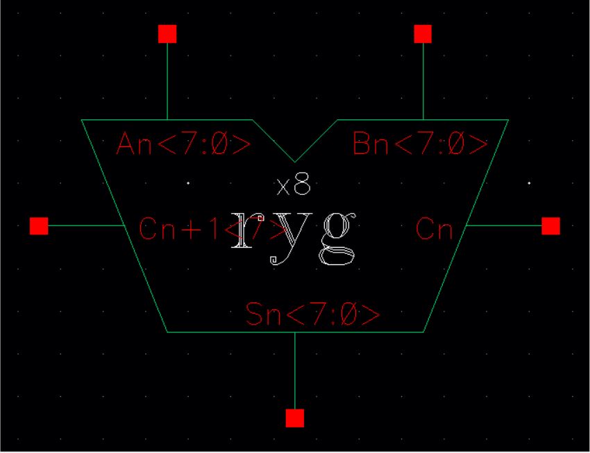 |  |


| 8-bit Full Adder Operation Simulation Schematic | 8-bit Full Adder Operation Simulation Output |
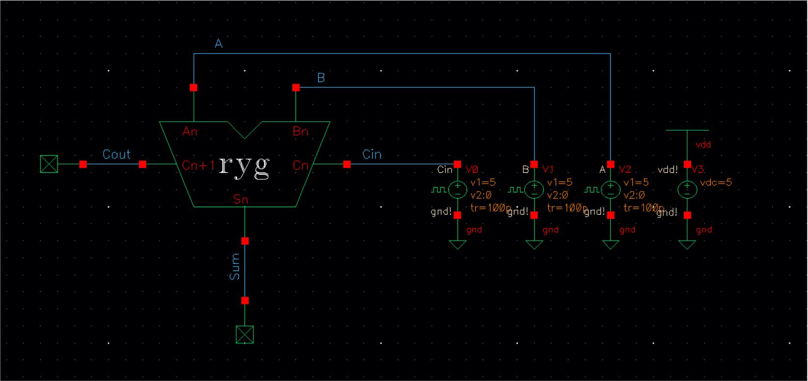 |  |
----------------------------------------------------------------------------------------------------
The design directory is downloaded from the MobaXterm server and backed up onto this website (Up-to-date 11/7/18).
-> They are stored into my backup folder on my laptop and also on my online drive.
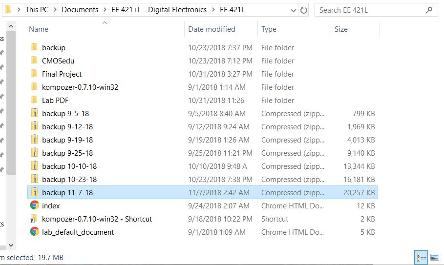
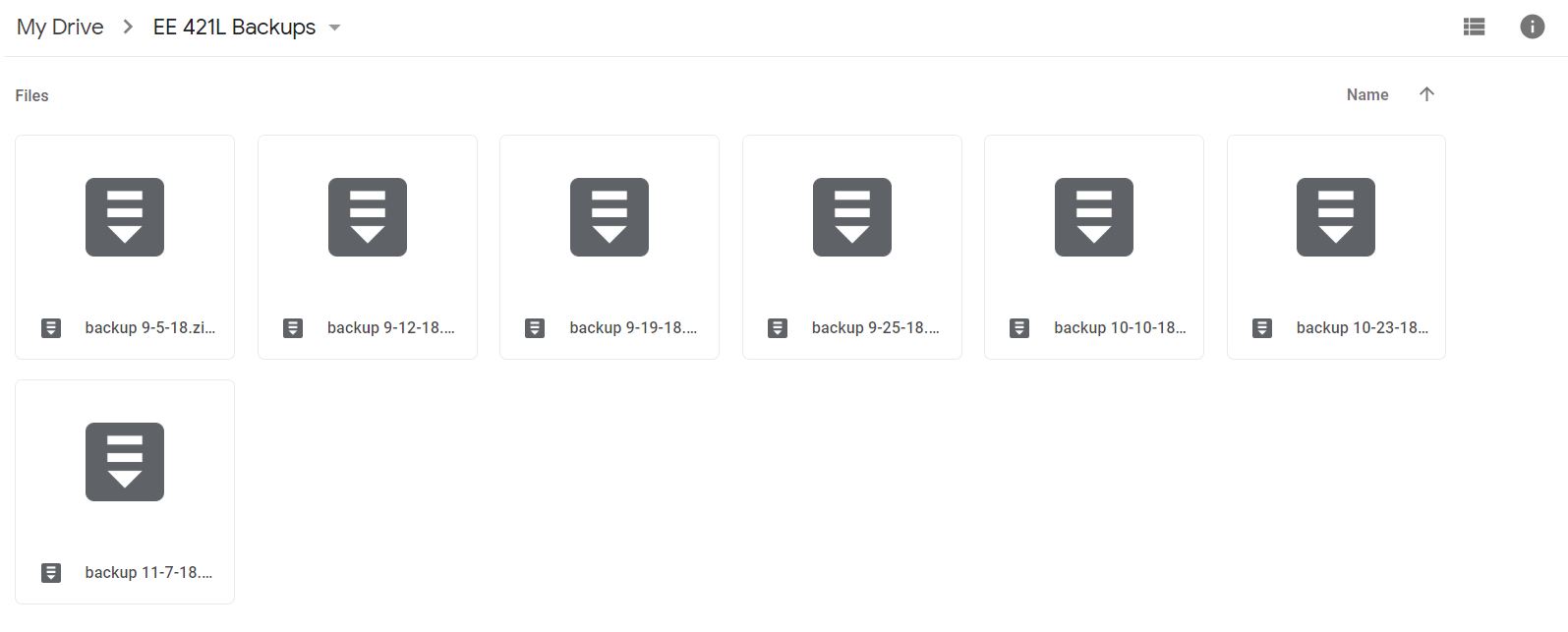
The CMOSedu directory has been backed up, and my following lab design directories will be continued to become backe up.
----------------------------------------------------------------------------------------------------
This Concludes the Lab 7 Report.