
12u/6u Inverter Schematic

48u/24u Inverter Schematic
Lab 5 - EE 421L
October 11, 2017
In this lab, we learned how to layout an inverter using a PMOS and a NMOS device. Two inverters were created for this lab. The first one had a PMOS with a width of 12u and a NMOS with width of 6u. Both of the MOSFET devices have a minumum width of 0.6u. A schematic for this device can be seen below. To create the second inverter, a multiplier of 4 was used on the PMOS and NMOS from the first design.
12u/6u Inverter Schematic | 48u/24u Inverter Schematic |
The next step was to create a layout, extract, and LVS for each inverter. Both inverters passed DRC and LVS. Pictures from this part can be seen below.
 12u/6u Inverter Layout |  48u/24u Inverter Layout |
 12u/6u Inverter Extracted |  48u/24u Inverter Extracted |
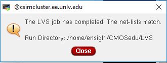 12u/6u Inverter LVS | 48u/24u Inverter LVS |